
 ?Mathematical formulae have been encoded as MathML and are displayed in this HTML version using MathJax in order to improve their display. Uncheck the box to turn MathJax off. This feature requires Javascript. Click on a formula to zoom.
Abstract
To address the slow scanning speed of the laser confocal method for scanning DNA chips, we designed and built a CCD image-based DNA chip scanner. A high-powered LED was selected as excitation light source. To avoid stray light in the optical path, we designed a light entrance, an extinction dark room, a diaphragm, and an extinctor that eliminated 99.95% of the stray light. A focal automatic calibration scheme is proposed; the only addition to the hardware was the focusing motor and the connection device between the motor and the lens. Furthermore, variance was used as the image sharpness evaluation function, with the combination of rough and fine calibration to increase real-time performance. An experiment showed that the accuracy of automatic focal calibration is higher than that of the manual method with repeatability error of 2.1%, and the time required is between 18.72 and 55.78 s. The sensitivity can reach 1.12 flour/µm2 with a resolution of 10.04 µm. Using the proposed scanner and a commercial Boao scanner on a fluorescence dot on the same genetic defect chip found a consistency coefficient of 0.95. The scanner has the advantage of simple hardware structure, quick detection, and favourite performance.
1. Introduction
The study of DNA chips (also known as gene chips) is rapidly emerging in the field of life sciences. DNA chips use the principle of complementary pairing between bases of nucleic acid molecules, fixes nucleotides to the support by various technologies, and then hybridizes with the processed samples to accomplish a large-scale test of sample genes. DNA chips can be widely used in drug research, disease diagnosis, gene structure, and functional research (Radom & Formanowicz, Citation2018; Saifullah, Fuke, Nagasawa, & Tsukahara, Citation2019; Sánchez-Pla, Citation2014). To convert biochemical reactions on DNA chips into meaningful information, a DNA chip scanner is required (Li et al., Citation2018).
DNA chip technology is accompanied by the development of research of genes, which meets the human needs for the exploration of genes. The in-depth research and extensive application of biochip technology represented by gene chips will have a profound impact on human life and health.
Affair is one of the first companies to conduct DNA chip technology research. The GeneChip Scanner 3000 7G developed by the company has a maximum detection sensitivity of 0.5 flour/um2 and a detection time of 5–10.5 min. The SureScan Microarray Scanner from Agilent's gene chip scanner has a maximum resolution of 2µm, and it takes 24 min to scan the chip with this precision. Axon Instruments’ GenePix series scanners are adjustable from 5 to 100 µm and take a 6.5 min dual-channel scan rate at 10 µm resolution. Beijing Boao has made great progress in the development and commercialization of array chip scanners. The company's crystal core LuxScan series chip scanner has a detection resolution of up to 5µm and a detection speed of 30s/cm2.
The two main methods for gene chip detection are the laser confocal method based on a photomultiplier tube, and the imaging method based on a charge-coupled device (CCD) combined with a high-pressure xenon or mercury lamp. The laser confocal method focuses the laser to an area of a few micrometers and scans back and forth on the chip to excite a single pixel. The result is then converted into a digital signal by a photomultiplier tube. The CCD imaging method filters the light source into a narrow-band wavelength range, irradiates a large area of the chip, excites a fluorescent marker to generate fluorescence, and then captures the image with a CCD camera (Bayrak & Oğul, Citation2019). The laser confocal method has the advantage of high sensitivity. However, the detection duration is long because the probe must be scanned point by point. Also, the hardware structure is complicated, increasing the difficulties of manufacturing, maintenance, and popularization. The CCD method can image all at once, shortening the detection duration, but there are stringent requirements for the design of the light source and the elimination of stray light in the optical path (Yin et al., Citation2018).
However, with the rapid development of semiconductor technology, the development of high-power LEDs and high-sensitivity CCDs has increased significantly. Therefore, in our study we abandoned the traditional high-pressure xenon or mercury lamp method to avoid the disadvantages of high heat generation, short working life, and high price. By adopting a high-powered LED light source and designing a closely matched optical path, we built the proposed DNA chip scanner.
In a CCD-based scanner, because the imaging lens focus is very sensitive, the lens can easily become out of focus when the instrument is moved or the glass loading platform is loaded or unloaded, blurring the captured image. Manual focus calibration is difficult to operate, time-consuming, and cumbersome. We propose a simple and easy-to-use focusing hardware structure that has only a slight change on the original structure of the scanner. We studied the image sharpness evaluation function, the calibration window selection, and the focal search strategy to fulfil the automatic focus calibration requirement.
The rest of the paper is organized as followed: The design process of the DNA chip scanner is introduced in Section II. In Section III, we focus on the research on automatic focal calibration. The performance evaluation of scanner with automatic focus calibration is given in Section IV. Finally, Section V concludes the paper.
2. Hardware design of the image-based gene scanner
2.1. Scanner structure
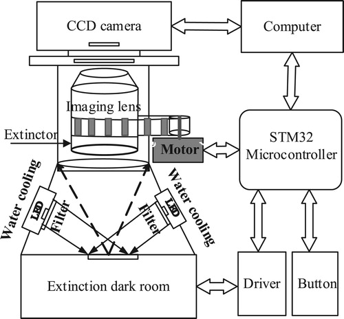
The proposed scanner comprises a light source, a matching optical path, and a control module. A schematic of the scanner is shown in Figure . High-powered LEDs are used as the light source. The red and green dual-channel high-powered LEDs are above and to the left and right sides of the chip. The LED light is irradiated onto the DNA chip through the curved lens and the filter. The stray light is absorbed, taken away, or blocked by the optical path, allowing the fluorescence emitted from the chip to be captured by the CCD camera. The control module uses an STM32 single chip (STMicroelectronics, Switzerland) to carry out functions such as the entry or exit of the glass loading platform, switching of the filter, and control of the focus calibration and button.
Figure 1. Schematic of the hardware structure of the proposed scanner.
2.2. Light source selection
It is difficult for a single LED to satisfy a gene scanner’s need for high intensity. However, an array of LEDs with multiple lamp beads will lead to low light utilization and a complicated optical lens design. After testing various light sources, we finally adopted the high-power LED light source PT54 (Luminus Devices Inc., USA), which has stable performance, high brightness, and a small light-emitting area, and can reach more than 30 W in 5 mm2. However, because the PT54 approximates the diffusion of a Lambertian source, the divergence angle of the light is large and the collimation is poor. Consequently, we use curved lenses according to the illuminance distribution characteristics of the PT54 light source. The lenses reduce the divergence angle of the light source and improve the utilization and collimation of the light.
2.3. Design of the optical path
The optical path of the scanner requires a combination of narrow-band filter sets. However, because the fluorescence intensity emitted from the gene chip is very weak compared with that of stray light, even high-performance narrow-band filters are not likely to filter stray light enough to prevent the fluorescence from being overwhelmed. The key to the light path design is to eliminate stray light.
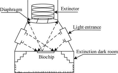
By extensive experiments and simulations, we found that the sources of stray light in the optical path were the multiple reflections from the area outside the biochip, the glass of the biochip, and the bottom of the instrument. Considering this, we adopted the scheme shown in Figure to eliminate stray light. It is composed of a light entrance, an extinction dark room, a diaphragm, and an extinctor.
Figure 2. Schematic of optical path structure to eliminate stray light.
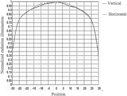
To simulate the designed optical path, we used OptisWorks software (ANSYS, USA) to trace 1 × 10⁴ rays. The light distribution is shown in Figure . After the light was irradiated onto the biochip, most of it was transmitted to the extinction dark room and reflected to the left area. A small amount of stray light was reflected and blocked by the diaphragm. Only a small amount of stray light could enter the camera and finally be filtered by the emission filter. The simulation results show that the stray light elimination efficiency of the optical path is 99.95%. The illumination distribution is shown in Figure . The illumination uniformity was greater than 92% in the 30 mm × 30 mm central area of the gene chip. By these specifically designed optical paths and filters, stray light was effectively eliminated.
Figure 3. Schematic diagram of optical path simulation results.
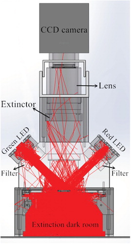
Figure 4. Illumination distribution result from optical path simulation.
2.4. Design of automatic focus calibration
Manual focus calibration has many shortcomings, so in this study we designed an automatic focus calibration.
The focus can be calibrated by adjusting the image distance, the object distance, or the focus of the imaging lens. Adjusting the image distance changes the back intercept of the imaging system, destroying the integrity of the CCD and the imaging lens. However, adjusting the object distance, generally by moving up and down the glass loading platform of the biochip, has two drawbacks. One is that achieving control of the platform’s up and down movement requires much more complex hardware. The other is that adjusting the object distance changes the imaging ratio and decreases the efficiency of the fluorescence collection (Xiao, Di, Zhu, Wang, & Xu, Citation2016). Adjusting the focus of the imaging lens only requires an additional focusing motor and a connector between the motor and the lens, but it has the advantages of low cost and little effect on the scanner, so we chose it as the focus calibration scheme in this study. Furthermore, a limit switch is used to ensure that the calibration is within the focus range (Selek, Citation2016).
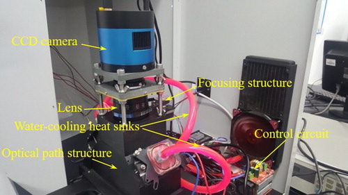
2.5. Scanner prototype
Both the instrument detection and the focal length autocalibration process require the camera to collect fluorescence images. We designed and built a scanner prototype that accommodated capturing weak fluorescence, a l imited camera price, and the reduction of the influence of thermal noise. The prototype consisted of a CCD camera (cooling type; Hangzhou ToupTek Photonics Co. Ltd, Zhejiang, P.R. China), a macro lens (V-DX 60-mm 2.8 2X MACRO, Anhui ChangGeng Optics Technology Co. Ltd, Hefei, P.R. China), an STM32 control board, and a focusing motor. The physical prototype of the designed scanner is shown in Figure . The black aluminium frame is the optical path structure of the scanner. The backs of the LEDs have water-cooling heat sinks. The upper part of the light path is a CCD camera. The lens and the focusing structure was on the rear side of the optical path structure. After much testing and analysis, we set the driving current of the focusing motor to 0.5 A and the subdivision accuracy of the driver to 400 pulses/circle.
Figure 5. Scanner physical prototype.
3. Research on automatic focal calibration
3.1. Comparison of evaluation function
It is necessary to determine the image sharpness in the focal calibration process to determine the state of the focus. We considered the spatial domain functions, including square gradient, Brenner, TenenGrad, and variance; the frequency domain (for example, Fourier transform); image entropy; and statistical functions (for example, Vollath’s) (Guo et al., Citation2017). The spatial domain evaluation function performs the definition calculation by analyzing the spatial characteristics of the image distribution. Compared with the blurred image, the clear image has sharper edges, the pixel values are more concentrated in spatial distribution, and the pixel value size difference is relatively large, so the clarity-evaluation can be performed according to the spatial features. The imaging system can be equivalent to a low-pass filter related to the cutoff frequency and the out-of-focus appearance, so the image can be first transformed from the spatial domain to the frequency domain, and the clarity-evaluation can be performed according to the high frequency component in the frequency domain. Compared with the blurred image, the gray image distribution of the clear image is more diverse and discrete, and the entropy of the image is smaller. Therefore, the clarity-evaluation can be performed according to the image entropy. The statistical evaluation function mainly determines the sharpness of the image by statistical characteristics of the pixel values of the image. It was necessary to evaluate the unimodality, sensitivity, noise resistance, and real-time performance of those functions for use in our system (Boscaro, Jacquir, Sanchez, Perdu, & Binczak, Citation2017).
Unimodality: The adjustable focal range of the imaging lens in our system was 60 mm. From one end of the lens to the other with 2.5-mm steps, a total of 25 images from blur to sharpness and then back to blur were obtained. The sharpnesses normalized to 100 are shown in Figure .
As can be seen from Figure , the image entropy violated unimodality. The square gradient, Brenner, and TenenGrad functions had only one maximum value in the entire focusing range, but they were not strictly monotonic and still violated unimodality. Only the variance, Vollath’s, and Fourier transform functions satisfied unimodality in the focusing range.
Sensitivity: The sum of the focus sensitivity values of 24 defocus images according to Equation (1) was used to measure the sensitivity of the evaluation function:
(1)
The sensitivity values of the variance, Vollath’s, and Fourier transform functions were 244.78, 305.26, and 114.49 respectively. The sensitivity of the Fourier transform function was the best, but its advantage over the variance function is not obvious.
Real-time performance: We used real-time performance to measure the complexity and processing efficiency of the image sharpness evaluation. The process of automatic focus calibration must evaluate tens of images. For the variance, Vollath’s, and Fourier transform functions the average consumed times for the 25 pictures were 0.92, 0.71, and 1.65 s/sheet respectively in the rough process. The computer used had an Intel Core i5 processor with a frequency of 2.20 GHz and a memory of 4GB. Because the Fourier transform function must convert the image from the spatial domain to the frequency domain and then analyze it, that function takes the most time. The variance function calculates the grey level distribution of the image in the spatial domain, which takes less time. The Vollath’s function calculates only pixels of images in the spatial domain, so it takes the least time.
Noise resistance: The CCD camera was subjected to mainly Gaussian noise in shooting. In this study, a Gaussian noise with a 0 mean and 0.1 variance was added to the image sequences. The normalized sharpness evaluation values of the variance, Vollath’s, and Fourier transform functions are shown in Figure .
Figure 6. Sharpness evaluation function curve.
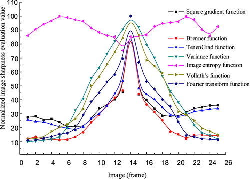
Figure 7. Image sharpness evaluation curve after adding noise.
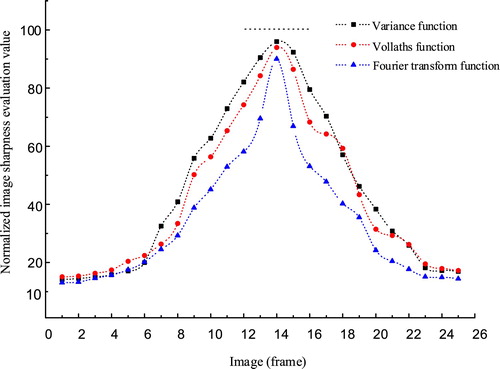
After comparing the unimodality, sensitivity, antinoise, and real-time performance, we used the variance function for the focal calibration in this study.
3.2. Selection of focal calibration window
In the process of focal calibration, the selection of the calibration window is involved in the evaluation of sharpness; this can be an adaptive selection or a fixed-area selection. An adaptive selection is suitable for applications when the focus image is not fixed. The process is complicated and requires much calculation. A fixed-area selection selects one or more areas fixed on the image as evaluation areas, usually used in the fixed foreground target of the focus image. It has the advantage of a simple and small calculation (Cabazos-Marín & Álvarez-Borrego, Citation2018). In this study, we used a fixed nano-fluorescence calibration chip to calibrate the focus. The calibration image is shown in Figure . A fixed-fluorescence dot matrix area can adequately distinguish the sharpness of an image, so the fixed area selection was more suitable for the scanner.
Figure 8. Triple-fluorescence calibration chip image.
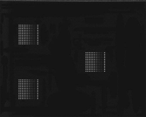
After determining the fixed area selection, we had to consider whether to select the triple-fluorescence dot matrix window (namely the whole image) shown in Figure or the single-fluorescence dot matrix window shown in Figure as the sharpness evaluation region. To compare the above two methods, we calculated the variance function of the rough focus; the results are shown in Figure .
Figure 9. Single-fluorescence dot matrix image.
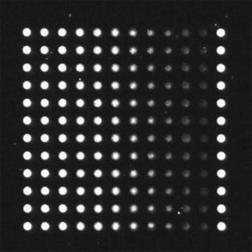
Figure 10. Sharpness comparison of single-fluorescence dot matrix and triple-fluorescence dot matrix.
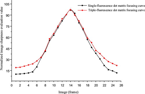
Regardless of whether a single-fluorescence dot matrix or a triple-fluorescence dot matrix (the entire image) was selected as the image focal calibration window, the evaluation curves satisfied unimodality. The two curves were very close to each other near the exact focus position because the images contained a rich, useful fluorescent signal, so the evaluation values of the two curves were similar after normalization. When the focus was far from the exact focus position, the evaluation curve of the triple-fluorescence dot matrix rose. This is because the images of the two ends contained less useful information, and the triple-fluorescence dot matrix had a larger area and greater information, causing the higher evaluation value.
The amount of calculation required by the triple-fluorescence dot matrix was more than three times that of the single-fluorescence dot matrix. Tens of images need to be evaluated in the focusing process, so the single-fluorescence dot matrix area was of course chosen as the focal calibration window in the system.
3.3. The mountain climbing-based focusing step search strategy
To complete the automatic focus calibration process, in addition to improving the hardware and selecting the appropriate image sharpness evaluation function and calibration window, we had to decide how to control the step motor. How to determine an appropriate step size remains an open problem. To improve the real-time performance, we adopted a calibration that combined rough and fine procedures. That is, a large step was used first until it was near the exact focus position, then a small step was selected. Because the driving wheel modulus of the focusing step motor was 0.5 mm, the step size for fine calibration was fixed at 0.5 mm. After trial and error, we chose a 5-mm step for rough calibration.
After determining the step sizes, we devised a ‘mountain climbing’ search that included four steps: initial image acquisition, judgement of focus state, rough calibration, and fine calibration.
Initial image acquisition: Five frames of images symmetrically on both sides of the initial position with a rough step were collected, and the sharpness was evaluated as F(-2), F(-1), F(0), F(1), and F(2).
Judgement of focus state: If F(0) were the maximum of the five sharpness values, the clearest focus was at the initial position in the condition of rough calibration. Therefore, we could skip the rough calibration and go straight to the fine calibration. Otherwise, rough calibration was required and the direction had to be decided. If the values from F(-2) to F(2) monotonically ascended or descended, the rough calibration direction was toward the greater sharpness; otherwise, the rough calibration direction was toward the maximum value between F(-2) to F(2).
Rough calibration: First, two frames of images were collected along the calibration direction. If the sharpness evaluation of the kth frame image was greater than that of the latter two frames, the focus of the kth image was the exact focus position under rough calibration. Otherwise, the procedure was repeated until the condition was satisfied and the rough calibration was completed.
Fine calibration: The fine calibration procedure was similar to that of the first three steps, except that the calibration step was 0.5 mm. Because the focusing motor was step motor and its driving wheel modulus was 0.5 mm, the step size for fine calibration was fixed at 0.5 mm.
4. Performance evaluation of scanner with automatic focus calibration
4.1. Experimental design and analysis
First, the quality of an automatic focus calibration is measured by accuracy, repeatability error, and real-time performance. Then it is necessary to evaluate the detection performance of the entire instrument by four indexes: number of fluorescence channels, efficiency, sensitivity, and resolution. The image-based DNA chip scanner designed in this study has red and green dual channels, which is consistent with mainstream instruments. In terms of detection efficiency, because the image mode is used, the single-channel detection time scanning 30 mm × 30 mm probe area requires only 55 s, fewer than that of the laser confocal mode. So only the detection sensitivity and resolution were evaluated in the following experiments.
Finally, after automatically calibrating the focus to the exact position, we evaluated the detection performance of the scanner by comparing its results with those of other commercial instruments on the same DNA chip.
4.2. Automatic focus calibration
4.2.1. Accuracy of automatic focus calibration
We compared the sharpnesses of the fluorescence images with those of a manual focus calibration by the variance function to evaluate the accuracy of the automatic calibration. Therefore, we could obtain the results by collecting fluorescence images of two focusing modes and then comparing the image sharpness. The procedure was as follows:
Manually adjust the focus to the clearest position, collect the image of the fluorescence calibration chip, rotate the focus wheel randomly, automatically calibrate the focus to the exact position, and collect the calibration chip image again. The above procedure was repeated 10 times, and then we calculated the sharpnesses shown in Table .
Table 1. Normalized image sharpness evaluation.
Table shows that the normalized evaluation values of manual and automatic calibration were 98.2 and 99.7 respectively. The accuracy of automatic focus calibration was higher than that of manual focusing.
4.2.2. Repeatability error of automatic focus calibration
The repeatability error of focus calibration refers to the consistency of the obtained fluorescence images when the focus calibration is from the same position. It is measured by the average pixel value of the fluorescence dot matrix in the fluorescence image (the image bit depth is 16 bits). The repeatability error is calculated as (Hart, Zhao, Garg, Bolusani, & Marcotte, Citation2017)
(2)
(2) Where
and
are the maximum and minimum respectively,
is the average of the average pixel values, and n is the number of calibrations.
First, we adjusted the focus to the leftmost end of the focus range, and then did automatic focus calibration from that position and obtained the average pixel values. The procedure was repeated 10 times, and the results are shown in Table .
Table 2. Average pixel values.
The calibration repeatability error was R = 222/10,585 = 2.1%.
4.2.3. Real-time automatic focus performance
For the real-time evaluation, we calculated the time it took to automatically calibrate the focus to the exact position. The time required differed depending on the initial position, so we calculated the longest and shortest times to determine the range of focusing time.
To calculate the shortest time, we first adjusted the lens to the sharpest focus position and then manually made the instrument slightly out of focus. The focus was automatically calibrated again to the sharpest position, and the time consumed was recorded. The above procedure was repeated 10 times. The time consumed is shown in Table , which shows that the average shortest focusing time was .
Table 3. The shortest time consumed to automatically calibrate.
To determine the greatest duration, we first adjusted the focus to the leftmost end of the focal range. The focus was automatically calibrated, and the time consumed was recorded. This procedure was repeated 10 times. The times consumed are shown in Table , which shows that the average longest calibration time was .
Table 4. The longest time consumed to automatically calibrate.
The times required for the automatic focus calibration ranged from 18.72 s to 55.78 s. The image exposure and the motor operation took most of the time.
4.3. Detection sensitivity of the scanner
In this context, sensitivity is the extent to which an instrument can detect weak signals mixed with noise in units of flour/µm2 (number of fluorescent molecules per square micron). Sensitivity is usually defined as the smallest signal detectable when the signal-to-noise ratio (SNR) is greater than 3. The lower the detection limit, the greater the sensitivity of the detection device.
We used the FMB DS01 calibration chip (Full Moon BioSystems, USA) to examine the detection limits of our scanner. That calibration chip contains two arrays that produce CY3 and CY5 fluorescent dyes, each array consisting of 28 sets of CY3 or CY5 fluorescent dyes from low to high concentration, 3 sets of blanks, and a set of molecular markers for localization. Each column contains 12 replicated samples of the same concentration.
The following steps are done to evaluate scanner detection sensitivity:
Calibrate the focus to the exact position, and then position the FMB calibration chip.
Turn on the LED light and set the exposure time to ensure that the last four to five high-concentration dyes can produce a saturated signal.
Scan the chip with red and green LEDs.
Calculate SNR to identify the column with an SNR greater than or equal to 3.
Refer to the calibration chip manual to find the sensitivity that corresponds to that column.
Figure 11. Fluorescence image of the CY3 array.
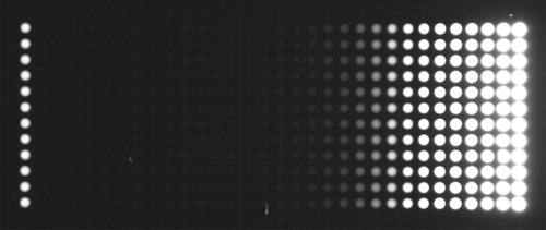
Figure 12. Fluorescence image of the CY5 array.
4.4. Detection resolution of the scanner
The fluorescence emitted by the DNA chip was captured by the imaging lens and the CCD camera, so for a clear fluorescent image it was necessary to ensure high resolution of the imaging system. A 1951 USAF resolution test chart (Figure ) can be used to measure the resolution level of a camera imaging system. The largest set of short lines on the chart that the imaging system can resolve is its resolution.
Figure 13. 1951 USAF resolution test chart image with enlargement of groups 2, 3, 4, and 5. (Group numbers are above the charts.).
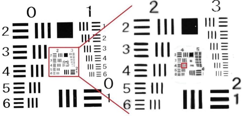
The test steps are as follows: Adjust the scanner’s receiving filter to the neutral position, calibrate the focus to the exact focus position, position the test chart, turn on the LED, and use the CCD camera to capture the picture. The resulting resolution chart image is shown in Figure . The relation between the short-line group and the specific resolution is shown in Table .
Table 5. Resolution corresponding size (µm).
Figure shows that the fourth short line of the fourth group could be clearly distinguished, and because the imaging ratio of the scanner lens was 1:2.2, the resolution of the imaging system of the scanner was 22.1 µm/2.2 = 10.04 µm.
4.5. Test results of scanner comparison
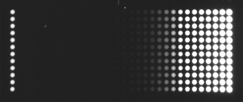
The CY5 channel was used to detect the genetic defect chip (Taipu COP; Triplex International Biosciences Co. Ltd, Xiamen, P.R. China) by comparing it using a commercial microarray chip scanner (Boao crystal core LuxScan 10 K; CapitalBio Technology Inc., Beijing, P.R. China). The Boao scanner and our scanner were exposed for 4 min and 55 s respectively, and microarray points of the obtained images are shown in Figures and respectively. In Figure , the pixel values of each fluorescent dot of the two images (image bit depth is 16) are plotted as the horizontal and vertical coordinates, and the linear relation is fitted with consistency coefficient R2 of 0.95.
Figure 14. Microarray points from proposed scanner test result.

Figure 15. Microarray points from Boao scanner test result.

Figure 16. Pixel point values of proposed scanner and Boao LuxScan 10 K scanner.
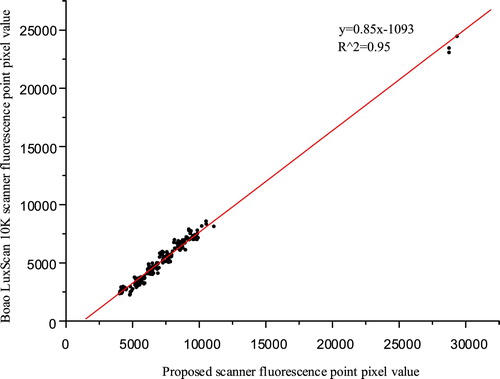
Both scanners could map the number of base pairs in the chip to the fluorescence intensity, and each fluorescent spot could be clearly distinguished from the background. The fluorescence intensity detected by the Boao scanner was greater than that of our scanner because the time taken to detect the two images was different. The fluorescence was attenuated when the duration was greater. In addition, because the Boao scanner adopted the laser confocal method, the background of the scanned image was darker. Our scanner can achieve the same effect by background image processing.
5. Conclusion
In this study, we successfully designed and implemented an image-based DNA chip scanner with automatic focus calibration by adopting a high-power LED light source and designing an accurately matched optical path. Also, to calibrate the focus, we propose an automatic calibration scheme; the only addition to the hardware is a focusing step motor and a connector between the motor and the lens. Furthermore, we used variance as an image sharpness evaluation function, and to increase real-time performance we used a focus search strategy combining rough and fine calibration. Results of scanning the same genetic defect chip with the proposed scanner and a commercial Boao scanner were highly consistent. The hardware structure of the scanner is simple, facilitating its manufacture, maintenance, and popularization.
Furthermore, there are still some future improvements. Firstly, the stray light in the optical path can be further reduced by using a material that absorbs light more easily or by using a professional light absorbing paint on the inner surface of the optical path structure. In the future, miniature motor and gear can be used to calibrate the focal length to improve the accuracy of calibration. Finally, we will enable the LED light intensity and temperature of the scanner to be controlled automatically to further increase its flexibility and degree of automation. It can further improve the performance of the instrument by using advanced image processing technology (Zeng et al., Citation2017; Zeng et al., Citation2018).
Disclosure statement
No potential conflict of interest was reported by the authors.
Additional information
Funding
References
- Bayrak, T., & Oğul, H. (2019). A New Approach for Predicting the value of gene Expression: Two-way Collaborative Filtering. Current Bioinformatics, 14(6), 480–490. doi: 10.2174/1574893614666190126144139
- Boscaro, A., Jacquir, S., Sanchez, K., Perdu, P., & Binczak, S. (2017). Pattern image enhancement by automatic focus correction. Microelectronics Reliability, 76-77, 249–254. doi: 10.1016/j.microrel.2017.07.012
- Cabazos-Marín, A. R., & Álvarez-Borrego, J. (2018). Automatic focus and fusion image algorithm using nonlinear correlation: Image quality evaluation. Optik, 164, 224–242. doi: 10.1016/j.ijleo.2018.02.101
- Guo, Z., Xie, N., He, P., Wang, X.-l., Chen, J., & Xu, R.-q. (2017). Design of experiment system for focal length Measurement of lens based on CCD. Computer Technology and Development, 27(5), 174–178.
- Hart, T., Zhao, A., Garg, A., Bolusani, S., & Marcotte, E. M. (2017). Human cell chips: Adapting DNA microarray spotting technology to cell-based imaging assays. PLoS ONE, 4(10), 1–7.
- Li, Y., Chen, J., Jiang, L., Zeng, N., Jiang, H., & Du, M. (2018). The p53–Mdm2 regulation relationship under different radiation doses based on the continuous–discrete extended Kalman filter algorithm. Neurocomputing, 273, 230–236. doi: 10.1016/j.neucom.2017.08.016
- Radom, M., & Formanowicz, P. (2018). An Algorithm for Sequencing by Hybridization based on an Alternating DNA chip. Interdisciplinary Sciences: Computational Life Sciences, 10(3), 605–615.
- Saifullah, S., Fuke, S., Nagasawa, H., & Tsukahara, T. (2019). Single nucleotide recognition using a probes-on-carrier DNA chip. BioTechniques, 66(2), 73–78. doi: 10.2144/btn-2018-0088
- Sánchez-Pla, A. (2014). DNA Microarrays technology. Comprehensive Analytical Chemistry, 63, 1–23. doi: 10.1016/B978-0-444-62651-6.00001-5
- Selek, M. (2016). A New Autofocusing method based on brightness and Contrast for Color Cameras. Advances in Electrical and Computer Engineering, 16(4), 39–44. doi: 10.4316/AECE.2016.04006
- Xiao, Z., Di, H., Zhu, H., Wang, L., & Xu, Z. (2016). Research on automatic focusing technique based on image autocollimation. Optik, 127(1), 148–151. doi: 10.1016/j.ijleo.2015.10.037
- Yin, X., Jiang, G., & Song, S. (2018). Research on an automatic tracking strategy based on CCD image sensor in micromanipulation. IEEE Access, 6, 76374–76380. doi: 10.1109/ACCESS.2018.2882499
- Zeng, N., Zhang, H., Li, Y., Liang, J., Dobaie, A. M., et al. (2017). Denoising and deblurring gold immunochromatographic strip images via gradient projection algorithms. Neurocomputing, 247, 165–172. doi: 10.1016/j.neucom.2017.03.056
- Zeng, N., Zhang, H., Song, B., Liu, W., Li, Y., & Dobaie, A. M. (2018). Facial expression recognition via learning deep sparse autoencoders. Neurocomputing, 273, 643–649. doi: 10.1016/j.neucom.2017.08.043