
ABSTRACT
Obvious grain growth was observed in regions around the fatigue cracks in the Au thin films under cyclic loading. Dominant generation of twin boundaries (TBs) and low-angle grain boundaries was observed in the coarsened grains. The experimental evidence shows that the newly formed TBs are mainly incoherent TBs, rather than the classical coherent TBs.
GRAPHICAL ABSTRACT
IMPACT STATEMENT
A number of newly formed twin boundaries (TBs) are observed to be mainly incoherent TBs rather than the classical coherent TBs in the coarsened grains of the fatigued Au film.
The grain boundary (GB) microstructure is a key factor to control the performance of metallic materials, such as mechanical properties, corrosion resistance, diffusion and electrical conductivities. With low mobility, low boundary energy and the minimum scattering of conducting electrons, twin boundaries (TBs) and low-angle GB (LAGBs) are preferential choices for microstructure control.[Citation1–10] However, such really special boundaries only constitute a very small group among all the boundaries in polycrystalline metals due to the restriction of thermodynamic equilibrium.[Citation11] Till date, GB engineering has been developed to optimize material microstructures,[Citation4,Citation12] such as rapid-solidification,[Citation13] thermalmechanical method,[Citation14,Citation15] annealing,[Citation16]electrodeposition,[Citation1,Citation2,Citation17] sputtering,[Citation6,Citation17] processing under plastic [Citation3,Citation18] and magnetic fields.[Citation19] Recently, researchers have succeeded in fabricating ultrastable materials with high-density TBs [Citation1,Citation2,Citation6] or LAGBs,[Citation3] which show excellent mechanical properties.[Citation1–8,Citation10] Nevertheless, difficulties in producing large bulk structural components for practical services potentially drive much effort to look for new principles of creating dominant generation of the special boundaries (especially LAGBs and TBs).
Thermodynamic considerations indicate that some specific misorientation would appear or disappear to reduce the overall energy of the system during grain growth. This can be evidenced by the preferred generation of the LAGB from the high angle GB during nanocrystalline grain growth under mechanically loading.[Citation20–23] It implies that the mechanically driven microstructure instability could be utilized for the GB microstructure control.
Twins form as the production of grain growth, heat treatment (like annealing) or mechanical deformation.[Citation17,Citation24–30] The most frequently observed and discussed types of TBs in face-centered-cubic (fcc) metals include (i) the low-energy coherent TB (CTB) across which a mirror image of atoms can be seen; (ii) the incoherent TB (ITB) with high boundary energy where there is a partial dislocation on each slip plane. Due to the low GB energy, the CTB is the most favorable TB during grain growth. However, subnanometer resolution inverse pole figure orientation mapping recently revealed that many as-grown CTB is generally defective with kink-like steps and curvature.[Citation31] These imperfections consist of incoherent segments and partial dislocations.[Citation25,Citation26,Citation28,Citation31] Here, we raise the question that whether the ITB can be the dominant TB during the mechanically driven grain growth. In this work, we present experimental evidence for the dominant formation of ITBs during grain growth in nanocrystalline Au films under cyclic loading.
Experimental
We deposited Au films (target purity: 99.99%) with a thickness of 930 nm onto the 125 µm-thick polyimide (Dupont Kapton®) substrates using direct curret (DC) magnetron sputtering (Denton sputtering system) under ultra-high vacuum (10−7 torr) with the working pressure of 0.4 Pa. Before the deposition, the substrate was cleaned by sputtering Ar ions for about 5 min to remove the surface contamination and to improve the bond between the substrate and the film. The samples for HRTEM and TEM investigations were mechanically ground from the substrate side to ∼30 µm in thickness, and then further thinned from the substrate side by ion milling on a precision ion polishing system (Gatan 691) at −100°C.
Fatigue testing of the film samples with a gauge section of 13 mm in length and 3 mm in width was performed under load control with a frequency of 20 Hz and a load ratio (the minimum load/the maximum load) of 0.1. A real-time electrical resistance of the film was measured during cyclic loading to determine the number of cycles to failure of the Au film. More details of the fatigue testing can be found in our former work.[Citation32]
The texture of the as-deposited film was measured by X-ray diffraction θ–2θ scans under a Rigaku X-ray diffractometer D/MAX–2500/PC equipped with CuKα radiation (56 kV, 182 mA). Orientations of the coarsened grains along the fatigue cracks were measured by electron backscatter diffraction (EBSD) mapping in an EBSD system (HKL, Channel 5) in field-emission scanning electron microscopy (SEM, Zeiss Supra 35). The area of each EBSD mapping was about 90 µm2 with step intervals of 0.05 µm. Damage morphologies of the films were characterized by Zeiss Supra 35 SEM and field-emission transmission electron microscopy (TEM, FEI Tecnai F20).
Microstructural characterization
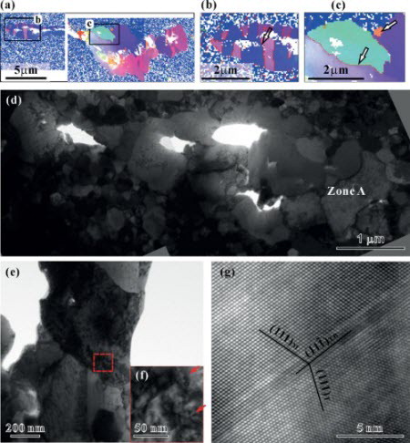
The as-deposited Au film studied here consists of near-columnar grains with a mean in-plane grain size of 52 ± 20 nm, as shown in Figure (a) and (b). X-ray diffraction θ–2θ scans (see Figure (c)) reveal that the film has a strong out-of-plane texture. We firstly examined the film sample, in which multiple cracks had appeared after 2.60 × 10⁴ cycles under a total strain range of 1.25%. Figure (d) presents a typical fatigue damage morphology which mainly exhibits multiple cracks, which are almost normal to the loading direction. The cracks generally initiated in locations with bulk-like fatigue extrusions/intrusions. The EBSD orientation mapping of the post-fatigued Au films in Figure (a) shows that grains along the fatigue crack had grown to several microns. These coarsened grains could essentially provide enough space for dislocation motion,[Citation33,Citation34] which explains why we could observe the severe surface extrusions/intrusions in the nanocrystalline films (see Figure (d)). Besides, we can observe many twins formed in the fatigued Au film, as indicated by arrows in Figure (b) and (c). However, we failed to find any typical newly formed wide twins under quantitative TEM observations (see Figure (d)) but some narrow twins in the coarsened grains (see Figure (e)–(g)).
Figure 1. (a) Cross-sectional TEM image of the 930-nm-thick Au film on the polyimide substrate. (b) Plan-view TEM image of the Au film. (c) The XRD θ–2θ scanning result of Au films, revealing the strong (111) out-of-plane texture. (d) SEM observation of the damage morphology in the post-fatigued Au films.
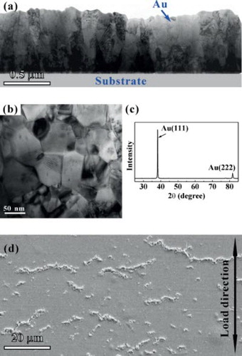
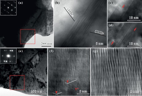
Figure 2. (a) EBSD orientation mapping of the cracked regions in the fatigued 930-nm-thick Au film. The white spots are areas with zero resolution. (b) and (c) Local magnification of the framed twinned areas in (a). The red lines present the TBs as indicated by the arrows. (d) TEM image of the coarsened grains along the cracks in the fatigued Au film. (e) TEM image of the typical grains with thin twin laminas in the fatigued Au film. (g) HRTEM image of the twinned area in (f). The twin relationship is marked by the solid line.
Dominant generation of ITB during grain growth
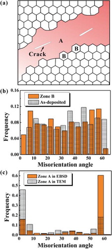
Using the Kikuchi pattern analysis under TEM,[Citation35] we characterized GB features in different zones in the fatigued sample, i.e. zone A represents the location along the well-developed crack with a length up to micron size (see Figure (d)), and zone B is the place around zone A, as illustrated in Figure (a). It is shown that only zone A did have an evident change in the distribution of GB misorientation angles, as shown in Figure (b) and (c). This indicates that it is associated with large stress concentration ahead of the crack tip. Interestingly, both TEM and EBSD characterizations (see Figure (c)) reveal the same trend in the misorientation distribution, that is, misorientation angles not only below 15° (LAGB) but also around 60° took a dominant proportion (85.1% for EBSD, 78.4% for TEM) in zone A. The 60°-misorientation angle in the coarsened grains is mainly corresponding to the appearance of the twin-relationship misorientation, as shown in Figure (a)–(c). The similar misorientation distribution under both TEM and EBSD characterizations indicates that the TEM observations did capture the images of the newly formed twins. These coarsened grains with TBs are just not of typical features of growth/annealing twins which have a lath shape and a rectilinear boundary commonly observed in metals with low-to-medium stacking fault energy.[Citation2,Citation17,Citation29] The following examples bring insight into features of the observed TBs between the coarsened grains along the fatigue cracks.
Figure 3. (a) Schematic illustration of positions of zone A and zone B in the cracked Au film after fatigue loading. Statistical distributions of normalized frequency of the misorientation angles of (b) the as-deposited films determined by EBSD and zone B in the fatigued Au film determined by TEM and (c) coarsened grains (zone A) determined by TEM and EBSD.
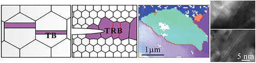
We can summarize from our EBSD orientation mapping images that there are two types of TBs: type A-TB is almost macroscopically rectilinear, and the intersection line of TB plane and the film surface is almost parallel to that of the plane and the film surface, as shown in Figure (b); type B-TB is curved and looks like a general GB, as shown in Figure (c).
Twinning mechanisms
Figure (a) shows a TEM image of the A-TB identified by the corresponding selected-area electron diffraction pattern. The close observation (Figure (b)) on the A-TB in Figure (a) shows that Moiré fringes are visible almost parallel to the A-TB. Obviously, the A-TB is not a CTB which is perpendicular to the specimen surface. On the contrary, the A-TB is an ITB. The production of growth twins during the grain growth is to reduce boundary energy; so it is reasonable to have dominant generation of growth twins with the low-energy CTB rather than the high-energy ITB. Thus, the newly formed twins in the coarsened grains are apparently not growth twins, they are deformation twins instead. The high stress at the crack tip not only caused grain growth but also deformation twins.[Citation36,Citation37]
Figure 4. (a) and (e) TEM images of two typical large grains with the twin misorientation in the fatigued Au film. The insets in (a) and (e) are the corresponding selected-area electron diffraction pattern of the framed areas. (b–d) and (f, g) The corresponding details of the framed areas in (a) and (e), respectively. The long arrows in (c) and (d) indicate the boundary steps. The short arrows in (f) indicate the positions of the intersection between the boundary and the right grain. The dotted lines indicate the pane of the left grains. The twin relationship is marked by the solid line. A perfect dislocation is indicated by a symbol ‘⊥’.
Repeatable patterns are clearly observed in the A-TB step, which has many units involving three planes, as shown in Figure (c) and (d). It was suggested that the deformation twins can form via the cooperative slip of three partials dislocations [Citation27,Citation28,Citation38–41]; thus there are bundles of partials on the front tip of the deformation twin, which is also an ITB. Due to a decrease in elastic energy and the low stacking fault energy of Au, the dissociation of the ITB was frequently observed, resulting in the emission of a Shockley partial dislocation on every third (111) planes from the initial compact ITB to produce a corresponding periodic array of stacking faults.[Citation28,Citation38,Citation39,Citation41,Citation42] Thus, we can observe the repeatable pattern in Figure (b)–(d).
Figure (e) shows a TEM image of the curved B-TB identified by the corresponding selected-area electron diffraction pattern. The B-TB has an almost 28°-deviation from the CTB. The close observations (Figure (f) and (g)) show a more complex faulted B-TB, which indicates that the B-TB planes are also not perpendicular to the specimen surface. As discussed above, the curved B-TB is also an ITB and such twin is also a deformation twin. Grain rotation and GB sliding during grain growth of the nanocrystalline Au film would alter local stress.[Citation43] These local stress variations were believed to promote the random emission of partials to form a deformation twin, in which partial dislocations with different Burgers vectors are randomly activated one after another.[Citation27,Citation44] Thus, we can observe irregular patterns of the boundary structure compared with the A-TB,[Citation45] as shown in Figure (c)–(d) and (f-g).
Figure (c) shows the growth evolution of the twin with highly curved TBs. A small-sized twin is formed near boundaries between the nano/submicron-sized grains and the coarsened grains in zone A, as indicated by the right arrow in Figure (c). The left twin with so many TBs had already grown to several micron-size, and stopped in the matrix grain interiors, as shown in Figure (c). Obviously, the nanocrystalline GBs as effective sources of twining partials [Citation46–49] played an important role in the twin formation. Besides, grain growth associated with grain rotation and sliding would promote the partial emission.[Citation44] GB migration would also be involved in grain growth to combine the small neighbor grains. During the migration process, the local GB environment would be changed,[Citation50–52] which would promote the emission of the partial along with local changes in GB orientation, GB structure and GB dislocation distribution.[Citation50,Citation53,Citation54] Furthermore, coupled with the high stress concentration at the crack tip, numerous twinning partials would be emitted from the GBs to form a twin. Thus, successive emission of partials would happen during the grain growth process, so that we can observe the highly curved TB with so many TBs connected by ITBs, as shown in Figure (c). The twining mechanism may be associated with both the coordinated slip of three partials and the random action of partials.
These TBs can be formed by three different mechanisms: (1) the coordinated slip of three partials (CSTP mechanism, e.g. Figure (c)); (2) the random action of partials (RAP mechanism, e.g. Figure (f)); (3) the cooperative mechanisms associated with the first two mechanisms (e.g. Figure (c)). The local stress state has been found to be crucial in the activation of the RAP mechanism and the CSTP mechanism.[Citation27,Citation39,Citation40,Citation44] The former mechanism happens when the local stress orientation changes.[Citation27,Citation44] In contrast, if the local stress remains unidirectional without change in orientation, CSTP mechanism will be also favored to produce twins.[Citation27,Citation39,Citation40] Both the cooperative activation of partials and the random nucleation of partials would relieve local stress concentration in the crack tip.[Citation40,Citation44] The competing relationship and the individual percent of twins formed by different mechanisms would be clarified in the future.
In summary, we have found that in addition to LAGBs, a number of TBs are preferentially formed in the coarsened grains driven by the stress concentration at the fatigue crack tip in nanocrystalline Au film. An interesting finding is that the newly formed twins do not show conventional growth twin features; instead they are identified to be deformation twins with a large number of ITBs. The findings may give rise to new clues for the designing and manipulating optimum GB microstructure to produce high-performance structural materials with specified GB characteristics.
Acknowledgements
The authors thank Dr W. Y. Wang, Mr X. G. Liu, Dr X. B. Hu, Prof. J. P. Cui, and Prof. C. B. Jiang for experimental supports.
Disclosure statement
No potential conflict of interest was reported by the authors.
Additional information
Funding
References
- Lu L. Ultrahigh strength and high electrical conductivity in copper. Science. 2004;304(5669):422–426. doi: 10.1126/science.1092905
- Lu L, Chen X, Huang X, Lu K. Revealing the maximum strength in nanotwinned copper. Science. 2009;323(5914):607–610. doi: 10.1126/science.1167641
- Liu XC, Zhang HW, Lu K. Strain-induced ultrahard and ultrastable nanolaminated structure in nickel. Science. 2013;342:337–340. doi: 10.1126/science.1242578
- Watanabe T. Grain boundary engineering: historical perspective and future prospects. J Mater Sci. 2011;46(12):4095–4115. doi: 10.1007/s10853-011-5393-z
- Bufford D, Wang H, Zhang X. High strength, epitaxial nanotwinned Ag films. Acta Mater. 2011;59(1):93–101. doi: 10.1016/j.actamat.2010.09.011
- Bufford D, Liu Y, Zhu Y, et al. Formation mechanisms of high-density growth twins in aluminum with high stacking-fault energy. Mater Res Lett. 2013;1(1):51–60. doi: 10.1080/21663831.2012.761654
- Idrissi H, Wang B, Colla MS, Raskin JP, Schryvers D, Pardoen T. Ultrahigh strain hardening in thin palladium films with nanoscale twins. Adv Mater. 2011;23(18):2119–2122. doi: 10.1002/adma.201004160
- Zhang X, Misra A, Wang H, et al. Enhanced hardening in Cu/330 stainless steel multilayers by nanoscale twinning. Acta Mater. 2004;52(4):995–1002. doi: 10.1016/j.actamat.2003.10.033
- Sansoz F, Lu K, Zhu T, Misra A. Strengthening and plasticity in nanotwinned metals. MRS Bull. 2016;41(4):292–297. doi: 10.1557/mrs.2016.60
- Li X, Dao M, Eberl C, Hodge AM, Gao H. Fracture, fatigue, and creep of nanotwinned metals. MRS Bull. 2016;41(4):298–304. doi: 10.1557/mrs.2016.65
- Priester L. Grain boundaries: from theory to engineering. Netherlands: Springer; 2013.
- Watanabe T, Tsurekawa S. The control of brittleness and development of desirable mechanical properties in polycrystalline systems by grain boundary engineering. Acta Mater. 1999;47(15-16):4171–4185. doi: 10.1016/S1359-6454(99)00275-X
- Watanabe T, Fujii H, Oikawa H, Arai KI. Grain boundaries in rapidly solidified and annealed Fe-6.5 mass% Si polycrystalline ribbons with high ductility. Acta Metall. 1989;37(3):941–952. doi: 10.1016/0001-6160(89)90021-7
- Tsurekawa S, Nakamichi S, Watanabe T. Correlation of grain boundary connectivity with grain boundary character distribution in austenitic stainless steel. Acta Mater. 2006;54(13):3617–3626. doi: 10.1016/j.actamat.2006.03.048
- Shimada M, Kokawa H, Wang ZJ, Sato YS, Karibe I. Optimization of grain boundary character distribution for intergranular corrosion resistant 304 stainless steel by twin-induced grain boundary engineering. Acta Mater. 2002;50(9):2331–2341. doi: 10.1016/S1359-6454(02)00064-2
- Kokawa H, Shimada M, Michiuchi M, Wang ZJ, Sato YS. Arrest of weld-decay in 304 austenitic stainless steel by twin-induced grain boundary engineering. Acta Mater. 2007;55(16):5401–5407. doi: 10.1016/j.actamat.2007.06.005
- Bufford DC, Wang YM, Liu Y, Lu L. Synthesis and microstructure of electrodeposited and sputtered nanotwinned face-centered-cubic metals. MRS Bull. 2016;41(4):286–291. doi: 10.1557/mrs.2016.62
- Bober DB, Kumar M, Rupert TJ. Nanocrystalline grain boundary engineering: Increasing Σ3 boundary fraction in pure Ni with thermomechanical treatments. Acta Mater. 2015;86:43–54. doi: 10.1016/j.actamat.2014.11.034
- Watanabe T, Tsurekawa S, Zhao X, Zuo L. Grain boundary engineering by magnetic field application. Scr. Mater. 2006;54(6):969–975. doi: 10.1016/j.scriptamat.2005.11.036
- Shan ZW, Knapp JA, Follstaedt DM, Stach EA, Wiezorek JMK, Mao SX. Inter- and intra-agglomerate fracture in nanocrystalline nickel. Phys Rev Lett. 2008;100(10):105502. doi: 10.1103/PhysRevLett.100.105502
- Shan ZW. Grain boundary-mediated plasticity in nanocrystalline nickel. Science. 2004;305(5684):654–657. doi: 10.1126/science.1098741
- Wang YB, Li BQ, Sui ML, Mao SX. Deformation-induced grain rotation and growth in nanocrystalline Ni. Appl Phys Lett. 2008;92(1):011903. doi: 10.1063/1.2828699
- Wang L, Teng J, Liu P, et al. Grain rotation mediated by grain boundary dislocations in nanocrystalline platinum. Nat Commun. 2014;5(5):4402:1–7.
- Mahajan S, Pande CS, Imam MA, Rath BB. Formation of annealing twins in f.c.c. crystals. Acta Mater. 1997;45(6):2633–2638. doi: 10.1016/S1359-6454(96)00336-9
- Liao XZ, Zhou F, Lavernia EJ, He DW, Zhu YT. Deformation twins in nanocrystalline Al. Appl Phys Lett. 2003;83(24):5062–5064. doi: 10.1063/1.1633975
- Zhu YT, Wu XL, Liao XZ, Narayan J, Mathaudhu SN, Kecskés LJ. Twinning partial multiplication at grain boundary in nanocrystalline fcc metals. Appl Phys Lett. 2009;95(3):031909. doi: 10.1063/1.3187539
- Wu F, Zhu YT, Narayan J. Macroscopic twinning strain in nanocrystalline Cu. Mater Res Lett. 2014;2(2):63–69. doi: 10.1080/21663831.2013.862874
- Wang J, Anderoglu O, Hirth JP, Misra A, Zhang X. Dislocation structures of Σ3 {112} twin boundaries in face centered cubic metals. Appl Phys Lett. 2009;95(2):021908. doi: 10.1063/1.3176979
- Zhu YT, Liao XZ, Wu XL. Deformation twinning in nanocrystalline materials. Prog Mater Sci. 2012;57(1):1–62. doi: 10.1016/j.pmatsci.2011.05.001
- Wang J, Zhang X. Twinning effects on strength and plasticity of metallic materials. MRS Bull. 2016;41(4):274–281. doi: 10.1557/mrs.2016.67
- Wang YM, Sansoz F, LaGrange T, et al. Defective twin boundaries in nanotwinned metals. Nat Mater. 2013;12(8):697–702. doi: 10.1038/nmat3646
- Luo XM, Zhu XF, Zhang GP. Nanotwin-assisted grain growth in nanocrystalline gold films under cyclic loading. Nat Commun. 2014;5(5):3021:1–8.
- Zhang GP, Volkert CA, Schwaiger R, Wellner P, Arzt E, Kraft O. Length-scale-controlled fatigue mechanisms in thin copper films. Acta Mater. 2006;54(11):3127–3139. doi: 10.1016/j.actamat.2006.03.013
- Boyce BL, Padilla HA. Anomalous fatigue behavior and fatigue-induced grain growth in nanocrystalline nickel alloys. Metall Mater Trans A. 2011;42(7):1793–1804. doi: 10.1007/s11661-011-0708-x
- Liu Q. A simple and rapid method for determining orientations and misorientations of crystalline specimens in TEM. Ultramicroscopy. 1995;60(1):81–89. doi: 10.1016/0304-3991(95)00049-7
- Farkas D, Willemann M, Hyde B. Atomistic mechanisms of fatigue in nanocrystalline metals. Phys Rev Lett. 2005;94(16):165502. doi: 10.1103/PhysRevLett.94.165502
- Cheng S, Zhao YH, Wang YM, et al. Structure modulation driven by cyclic deformation in nanocrystalline NiFe. Phys Rev Lett. 2010;104(25):255501. doi: 10.1103/PhysRevLett.104.255501
- Wang J, Li N, Anderoglu O, et al. Detwinning mechanisms for growth twins in face-centered cubic metals. Acta Mater. 2010;58(6):2262–2270. doi: 10.1016/j.actamat.2009.12.013
- Liu L, Wang J, Gong S, Mao S. High resolution transmission electron microscope observation of zero-strain deformation twinning mechanisms in Ag. Phys Rev Lett. 2011;106(17):175504. doi: 10.1103/PhysRevLett.106.175504
- Li BQ, Li B, Wang YB, Sui ML, Ma E. Twinning mechanism via synchronized activation of partial dislocations in face-centered-cubic materials. Scr Mater. 2011;64:852–855. doi: 10.1016/j.scriptamat.2011.01.016
- Li N, Wang J, Mao S, Wang H. In situ nanomechanical testing of twinned metals in a transmission electron microscope. MRS Bull. 2016;41(4):305–313. doi: 10.1557/mrs.2016.66
- Medlin DL, Campbell GH, Carter CB. Stacking defects in the 9R phase at an incoherent twin boundary in copper. Acta Mater. 1998;46(14):5135–5142. doi: 10.1016/S1359-6454(98)00164-5
- Meyers MA, Mishra A, Benson DJ. Mechanical properties of nanocrystalline materials. Prog Mater Sci. 2006;51(4):427–556. doi: 10.1016/j.pmatsci.2005.08.003
- Wu XL, Liao X, Srinivasan S, et al. New deformation twinning mechanism generates zero macroscopic strain in nanocrystalline metals. Phys Rev Lett. 2008;100:095701. doi: 10.1103/PhysRevLett.100.095701
- Zhang JY, Zhang P, Wang R, Liu G, Zhang G, Sun J. Grain-size-dependent zero-strain mechanism for twinning in copper. Phys Rev B. 2012;86(6):064110-1–6. doi: 10.1103/PhysRevB.86.064110
- Yamakov V, Wolf D, Phillpot SR, Mukherjee AK, Gleiter H. Dislocation processes in the deformation of nanocrystalline aluminium by molecular-dynamics simulation. Nat Mater. 2002;1(1):45–49. doi: 10.1038/nmat700
- Zhu YT, Liao XZ, Srinivasan SG, et al. Nucleation and growth of deformation twins in nanocrystalline aluminum. Appl Phys Lett. 2004;85(21):5049–5051. doi: 10.1063/1.1823042
- Liao XZ, Zhou F, Lavernia EJ, et al. Deformation mechanism in nanocrystalline Al: Partial dislocation slip. Appl Phys Lett. 2003;83(4):632–634. doi: 10.1063/1.1594836
- Liao XZ, Zhao YH, Srinivasan SG, Zhu YT, Valiev RZ, Gunderov DV. Deformation twinning in nanocrystalline copper at room temperature and low strain rate. Appl Phys Lett. 2004;84(4):592–594. doi: 10.1063/1.1644051
- Luo XM, Zhang B, Zhu XF, Zhou YT, Xiao TY, Zhang GP. Local-structure-affected behavior during self-driven grain boundary migration. MRS Commun. 2016;6(2):85–91. doi: 10.1557/mrc.2016.10
- Merkle KL, Thompson LJ. High-resolution electron microscopy of twist and general grain boundaries. Phys Rev Lett. 1999;83(3):556–559. doi: 10.1103/PhysRevLett.83.556
- Merkle KL, Thompson LJ, Phillipp F. Collective effects in grain boundary migration. Phys Rev Lett. 2002;88(22):225501-1–4. doi: 10.1103/PhysRevLett.88.225501
- Van Swygenhoven H, Derlet P. Grain-boundary sliding in nanocrystalline fcc metals. Phys Rev B. 2001;64(22):224105. doi: 10.1103/PhysRevB.64.224105
- Van Swygenhoven H, Derlet P, Hasnaoui A. Atomic mechanism for dislocation emission from nanosized grain boundaries. Phys Rev B. 2002;66(2):024101. doi: 10.1103/PhysRevB.66.024101