
ABSTRACT
We report on the self-assembly of core–shell Ge/In–Te nanowires (NWs) on single crystal Si substrates by Metalorganic Chemical Vapour Deposition (MOCVD), coupled to the Vapour–Liquid–Solid (VLS) mechanism, catalysed by Au nanoparticles (NPs). The NWs are formed by a crystalline Ge core and an InTe (II) shell, have diameters down to 15 nm and show <110> oriented growth direction. The role of the MOCVD process parameters and of the NPs size in determining the NWs core–shell microstructure and their alignment was investigated by high-resolution TEM, EDX, XRD and Raman spectroscopy.
GRAPHICAL ABSTRACT
IMPACT STATEMENT
A novel one-step MOCVD growth procedure, yielding self-assembled, oriented and crystalline core–shell Ge/In–Te nanowires with diameters down to 15 nm, along with their chemical–physical characterization.
1. Introduction
Developments in the synthesis of nanosized heterostructures are important for several applications, including electronics, chemistry, photonics and life science. Core–shell nanowires (NWs) with a Ge core represent a notable example of heterostructure and are investigated for the realization of, e.g. novel thermoelectric [Citation1] and memory [Citation2] devices. Also, quantum confinement and band offset between core and shell give rise to unique electrical [Citation3] and optical properties [Citation4] in NWs with a Ge core and a shell of a different semiconductor, such as Si. The Vapour–Liquid–Solid (VLS) mechanism, assisted by a metal catalyst and coupled to Metal Organic Chemical Vapour Deposition (MOCVD), is efficiently exploited for the growth of single phase NWs [Citation5–7]. While this method allows the bottom-up realization of free standing and oriented NWs with high crystal quality, the realization of a core–shell structure generally requires a two-steps growth process [Citation8,Citation9]. Another possible way for obtaining such fine nanostructuring is to take advantage of the immiscibility of the targeted phases. The In–Ge–Te phase diagram shows relatively limited regions of stable ternary compounds [Citation10], making this system a promising candidate for the spontaneous formation of Ge-based heterostructures. On the other hand, In–Te chalcogenide alloys possess several functionalities, from phase change memory [Citation11], to thermoelectric [Citation12] and nonlinear optical [Citation13] applications. The unprecedented introduction of a Ge core in In–Te NWs is expected to enable the realization of novel gas storage/sensing [Citation14], electronic and optoelectronic [Citation15] devices.
Here we describe for the first time the simultaneous synthesis of oriented core–shell Ge/In–Te NWs by a single step, bottom-up MOCVD process, based on the VLS mechanism and catalysed by Au nanoparticles (NPs). The morphology, orientation, composition and microstructure of the NWs as a function of the growth process parameters were investigated.
2. Experimental
The NWs growth was performed by an Aixtron® AIX 200/4 MOCVD reactor, exploiting the VLS mechanism induced by Au metal-catalyst NPs with average sizes of 10, 20, 30 and 50 nm, respectively. The Au NPs were dispersed from a colloidal solution by British Bio Cell Company® on Si (001), Si (111) and Si (110)—1 cm2—substrates, after removal of the Si native oxide by immersion in a HF 5% solution. The metalorganic precursors were electronic grade dimethylaminopropyl-dimethyl-Indium (C7H18InN, DADI), tetrakisdimethylamino germanium (Ge[N(CH3)2]4, TDMAGe) and bis(trimethylsilyl)telluride (Te(SiMe3)2, DSMTe), provided by Air Liquide® and were transported to the MOCVD reactor by an ultra-purified N2 carrier/process gas [Citation16]. The partial pressures in the vapour phase of DADI (PIn), TDMAGe (PGe) and DSMTe (PTe) were varied in the range 1.7 × 10⁻⁵ ÷ 1.0 × 10⁻³, 4.6 × 10⁻³ ÷ 5.4 × 10⁻² and 2.6 × 10⁻³ ÷ 6.4 × 10⁻² mbar, respectively, while the reactor temperature (TR) and reactor pressure (PR) were varied in the range of 360 ÷ 590°C and 300 ÷ 500 mbar, respectively. The deposition times ranged from 60 to 210 min. The morphology of the NWs was characterized by a Zeiss® Supra 40 field emission Scanning Electron Microscope (SEM). An ItalStructures® HRD3000 X-Ray Diffraction (XRD) system was used to evaluate the average crystal structure and growth orientation of the NWs. Their local microstructure, growth direction and composition were studied by High Resolution Transmission Electron Microscopy (HR-TEM), performed by a JEOL® 2200FS microscope with point resolution of 0.18 nm, equipped with an in-column Ω energy filter, 2 high-angle annular dark-field (HAADF) detectors and X-ray microanalysis (EDX). Confocal Raman microscopy was performed on both single and bunches of NWs in backscattering geometry at room temperature. The excitation wavelength was the 632.8 nm line of the HeNe laser. The power of the excitation was about 200 µW (equivalent to 40 kW/cm2). The laser beam was focused with a 100× objective (NA 0.80) and the scattered light was collected by a Horiba triple spectrometer equipped with 1800 g/mm gratings and liquid-nitrogen cooled multichannel charge couple device detector. The spectra were collected by selecting the scattered light polarized parallel to the polarization direction of the incident light in order to enhance the signal.
3. Results and discussion
Among all combinations of trialled MOCVD growth parameters, NW-like growth was obtained for PIn = 1.7 × 10⁻⁵ ÷ 1.0 × 10⁻⁴ mbar, PGe = 4.6 × 10⁻³ ÷ 2.6 × 10⁻² mbar, PTe = 2.6 × 10⁻³ ÷ 2.2 × 10⁻² mbar, TR = 375 ÷ 425°C and PR in the range of 400 ÷ 550 mbar. Outside this range, the growth led to the formation of nanostructures with poor quality or crystal agglomerates.
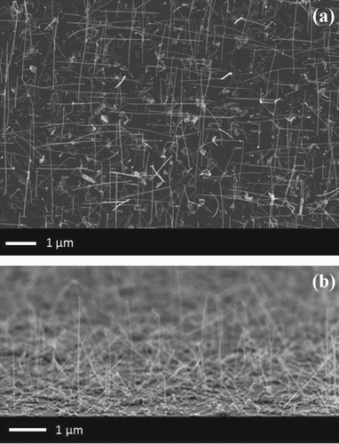
A very dense growth of NWs with lengths and diameters in the range of 1 ÷ 2 µm and 15 ÷ 30 nm, respectively, was obtained when using 10 or 20 nm Au NPs (Figure (a)). Systematic measurements of the inclination angles using top and side view SEM images showed that NWs are preferentially aligned along the <110> directions with respect to the Si (001) and Si (111) substrates. The same holds when Si (110) substrates are used, and a fraction of vertically aligned NWs was obtained in this case (Figure (b)). The possibility of controlling the orientation of the NWs by, e.g. epitaxy, can represent an important advantage for several of their applications [Citation17]. SEM observations also indicated that the density and degree of alignment of the NWs decrease with increasing the Au NPs sizes. Also, larger NPs produce NWs with larger diameters, consistently with the VLS growth mechanism.
Figure 1. SEM images of Ge/In–Te NWs grown on different substrates and catalysed by 20 nm Au NPs: (a) top view on Si (001); (b) tilted view on Si (110).
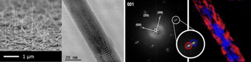
HR-TEM analysis revealed that the NWs synthesized with 10 and 20 nm Au NPs have a well-defined core–shell structure, where the core is composed by single crystalline Ge, surrounded by a crystalline In–Te shell. In Figure (a) the TEM micrograph of a core–shell NW oriented along the {001} zone axis is shown. The NW is grown along the <110> direction and has a well-defined, 10 nm wide core. In the picture, a squared Moiré pattern is clearly visible over the NW core, indicating a close relationship between the core and shell lattices, in terms of both orientation and lattice parameters. In the corresponding Fast Fourier Transform (FFT) shown in Figure (b), the pattern coincides with the [001] projection of cubic Ge and the stronger reflections have been labelled accordingly. The second set of spots, having comparable intensities, is perfectly aligned with that of the Ge lattice, but has a slightly larger lattice parameter, i.e. dGe200 = 2.86 Å and dInTe200 = 3.13 Å, in good agreement with the InTe (II) phase (ICSD card number 59547). The presence of crystalline phases in the NWs, along with the originated Moiré pattern, can be better appreciated from the HR-TEM micrographs of a second NW, shown in Figure (d) and (e). We measured the periodicity of the Moiré fringes formed by the superposition of the two parallel sets of planes, shown in Figure (e,f), and we found it consistent with the bulk lattice parameters of Ge and InTe (II) phases. Indeed, the Moiré fringes can here be used to demonstrate the absence of strain in the structure, at least within the limits of this technique. A careful investigation of the border region between the core and the shell revealed that there are a few crystallographic defects in the interface region of the core–shell structure, although their density is not enough to completely relax the lattice mismatch. Possibly, the roughness of the Ge/InTe interface may affect the strain relaxation [Citation18]. Another source of strain relief could come from a partial interdiffusion of Ge in InTe at the interface between the core and the shell, with the mismatch between the Ge and the InTe lattices being distributed over a few lattice parameters. While in the bulk the cubic InTe (II) phase is stable at high pressure only [Citation19], its presence in our core–shell nanostructures can be explained by a stabilizing effect due to the reduced dimensionality of the synthetized system and/or to the presence of the cubic Ge core. Also, the distribution map of the intensity pertinent to each spatial frequency (Figure (c)) clearly shows that the two signals are well separated: the Ge lattice is present only in the core region of the NW, while the InTe (II) is in the shell. The signals overlap, as expected, where the Moiré fringes appear.
Figure 2. (a) Low magnification TEM image of a {001} oriented core–shell NW. (b) FFT of (a). (c) Map representing in false colours the region where the InTe (red) and Ge (blue) phases are observed. The map is colour-coded according to the FFT magnification reported as inset. (d) High magnification TEM and (e) zoomed HR-TEM of a second {001} oriented core–shell NW. (f) Measurements of the periodicity of the Moiré fringes formed by the superposition of the parallel sets of planes.
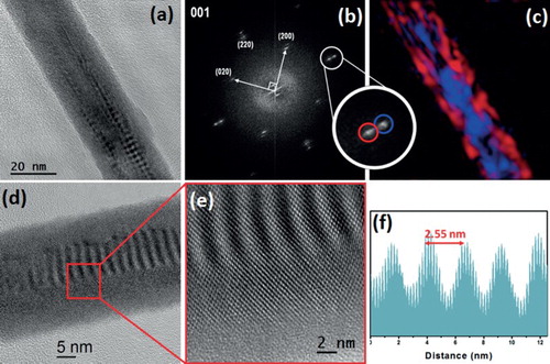
Figure 3. (a) STEM-HAADF image of a core–shell NW and its EDX map. The elemental maps of each atomic species are reported in (c)–(f), according to their labels (the markers correspond to 20 nm); the overall elemental map is shown in (b).
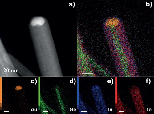
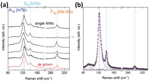
Figure 4. (a) Raman spectra obtained on an ensemble of as-grown NWs catalysed by 10 Au NPs on Si (001) (red solid line) and on 5 different single NWs transferred on a Si (111) substrate (black solid lines). Vertical dashed lines mark the frequencies of the modes related to InTe and Ge. (b) Raman spectrum of a representative single NW (open circles), with individual Lorentzian contributions deconvoluted (solid lines).
These results were also confirmed by the Scanning TEM (STEM)-EDX mapping. The reference STEM-HAADF image of a typical NW is reported in Figure (a), where the metal catalyst is also visible on the top of the NW. The elemental maps reported in Figure (c–f) show that In and Te are equally distributed in the shell; a local quantitative analysis reveals a 1:1 stoichiometry, in agreement with the previously reported structural analysis that indicated the presence of the InTe (II) phase. The Ge signal is instead mainly localized in the NW core, while only some random noise, comparable with the background, is visible in the shell. Finally, it is worth mentioning the amount of reactants detected (ex-situ) in the Au catalyst droplet, namely 30% of In, 10% of Te and 10% of Ge, as to confirm that all of the three elements are involved in the VLS mechanism. However, TEM analysis also revealed that not all the NWs exhibit the perfect core–shell structure described so far: a fraction of the NWs shows partial or complete intermixing of the Ge core and InTe shell. A statistic on forty NWs indicated that the fraction of NWs with a more pronounced intermixing of the Ge core and InTe shell increases with increasing the dimension of the catalysing Au NPs.
The good Raman signal, relatively narrow line shape and small frequency fluctuation also suggest that the InTe and Ge phases present in the NWs synthetized with the smallest Au NPs have good crystal quality (Figure ). The spectra taken on single NWs (dry-transferred on a Si substrate) and on the as-grown sample (containing both NWs and planar islands grown between NWs) have the expected three main modes, namely the A1g and Eg modes of InTe, at about 124 and 141 cm−1, respectively, and the F2g Ge–Ge optical mode at about 299 cm−1 (Figure (a)). Quantitative analysis performed on all spectra, as represented for a NW spectrum in Figure (b), revealed that the frequencies of three peaks vary less than 2 cm−1 from wire to wire and with respect to the as-grown sample, indicating the high homogeneity of the sample. The Raman measurements confirm the absence of strain in the wires: indeed a strained Ge core would lead to a shift of the frequency of the F2g phonon mode of Germanium, which is instead comparable to the bulk frequency within the experimental resolution [Citation20].
Furthermore, small compositional fluctuations within the shell cannot be excluded. While the low-intensity peak at about 85 cm−1 can be ascribed to the B1g symmetry [Citation21], the feature at about 103 cm−1 might indicate the presence of Ge–Te modes due to random diffusion of Ge into the shell [Citation22,Citation23]; their frequency is different in different wires/points, which could explain their broad band. Indeed, also the increased FWHM of the InTe-related peaks (from 8 to 10 cm−1) can be consistent with a compositional fluctuation or gradient at the core–shell interface. Such a compositional gradient can also support the above mentioned mechanism behind the strain release at the Ge/InTe interface.
XRD analyses in grazing incidence (ω = 1°) configuration were performed in order to quantify the amount of oriented NWs and evaluate the presence of spurious components. Figure (a–c) show the complete maps of significant in-plane rotations (Φ scans, with beam aligned along the Si <110> direction) for samples grown using 10, 20 or 50 nm Au NPs on Si (001) substrates. The 90° symmetry, typical of the <110> directions, is clearly evidenced for the most intense peaks. The peaks were identified as belonging to Ge and cubic InTe, with lattice parameters equal to 5.66 and 6.12 Å, respectively, in agreement with the TEM analysis and the ICSD database, thus suggesting that, despite the vicinity of the epitaxial relationship, the growth mechanism produces unstrained Ge/InTe core–shell NWs, or with a strain below the detection limit of the X-ray instrumentation employed for this work.
Figure 5. (a), (b) and (c) XRD Φ scans performed on samples with the same substrate size and NWs catalysed by 10, 20 and 50 nm Au NPs, respectively, showing the counts of plane [001] orientation of the NWs and their in-plane [110] orientation. (d) Some selected diffractograms obtained from a sample grown on Si (001) using 30 nm Au NPs. (e) Superposition for the samples grown on Si (001) using 10, 20, 30 and 50 nm Au NPs of the diffractograms obtained in front of the <110> direction (red) and at 45° from the <110> direction (blue).
![Figure 5. (a), (b) and (c) XRD Φ scans performed on samples with the same substrate size and NWs catalysed by 10, 20 and 50 nm Au NPs, respectively, showing the counts of plane [001] orientation of the NWs and their in-plane [110] orientation. (d) Some selected diffractograms obtained from a sample grown on Si (001) using 30 nm Au NPs. (e) Superposition for the samples grown on Si (001) using 10, 20, 30 and 50 nm Au NPs of the diffractograms obtained in front of the <110> direction (red) and at 45° from the <110> direction (blue).](/cms/asset/17519f6f-e7b3-4452-a0bb-4bb21f6aa7d2/tmrl_a_1384409_f0005_c.jpg)
The variation of the diffracted intensity as a function of Φ is also shown in Figure (d) for a sample grown using 30 nm Au NPs, while Figure (e) reports the superposition of the diffractograms in front of the <110> and 45° far from the <110> directions, for all the analysed samples grown on Si (001) substrates. As shown by Figure (a–d), the diffracted intensity varies as a function of the incidence angle, but some peaks are always visible. They correspond to randomly oriented NWs or to spurious agglomerates of crystals. For 10 nm Au NPs, the signal from the oriented InTe phase was barely observed. When increasing the Au NPs size, the signal from oriented Ge and InTe increases (for Ge (311) it saturates for 30 and 50 nm Au NPs), because of the contribution from bigger Ge/InTe NWs, as indicated by SEM and TEM observations. On the other hand, when increasing the size of the Au NPs, the amount of randomly oriented Ge and InTe increases too, as revealed by the spread in Φ of the diffracted intensity of the low angle peaks, confirming that the highest amount of free standing and oriented core–shell NWs is obtained with 10 and 20 nm Au NPs, and that, in the case of 10 nm Au NPs, the thinnest core–shell NWs are obtained.
The presence of the single crystalline Ge core can explain the strong directional growth of the core–shell NWs. Growth along the <110>, <111> and <112> directions has been observed before for the VLS synthesis of Ge NWs on single crystal substrates [Citation6,Citation7,Citation24]. For VLS-grown Si NWs a correlation has been found between the NWs diameter and catalyst size on the one hand, and the growth direction on the other, with small NWs diameter and catalyst sizes (below about 20–30 nm) favouring the <110> direction [Citation25,Citation26]. A common explanation for the observed preferential <110> growth direction in Ge and narrow-diameter Si NWs has been proposed in [Citation27], but there are no systematic studies in this respect in the literature. Our observation of highly oriented <110> growth only for the smallest size of Au NPs (10 and 20 nm) suggests the possibility of such a correlation also for Ge NWs.
Phase separation and formation of a core–shell structure have been reported in other VLS-grown NWs systems, such as InGaN NWs [Citation28], and in In-based chalcogenides, such as In–Sb–Te [Citation29] and In–Ge–Sb–Te [Citation30]. Nevertheless, the explanation of the processes leading to the core–shell structure of this work is not straightforward. The simplest path would involve the formation by VLS of the Ge core, which would serve as scaffold for the heterogeneous growth of the InTe shell, through a Vapour–Solid (VS) sidewall attachment. In this case, an increasing thickness of the InTe layer for increasing growth times would be expected. However, SEM and TEM analyses indicated that the thickness of the InTe shell does remain remarkably constant for different growth times and along the length of the NWs. Alternatively, being the range of existence of thermodynamically stable ternary phases in the In–Ge–Te phase diagram relatively small, it is possible that phase separation between Ge and InTe adds up to the VLS process and leads to the almost simultaneous formation of the core–shell structure. This picture is also consistent with the presence of all the three elements in the catalyst droplet, as revealed by TEM. The reason why such phase separation is particularly effective for the smallest size of the catalysts can be only speculated upon. It is possible that the diffusion time of the species (inward for Ge and outward for In and Te) allows a complete phase separation only for sufficiently small NWs diameters, before diffusion is frozen in by the solidification process. This would explain the larger fraction of NWs with incomplete or absent core–shell structure when large Au NPs are used. An additional factor for phase separation could be represented by the elastic strain. Stress generated at the curved surfaces of the NWs was used to explain the core–shell structure of VLS-grown AlGaN NWs in [Citation31], where it is pointed out that such a stress is expected to be significant at the nanometer scale. Moreover, the role of strain relief between the VLS growing NW and the substrate, leading to the segregation of some species and hence to a core–shell nanostructure in the InGaN system was observed, e.g. in [Citation32]. Both the above strain relieving mechanisms could be active in the formation of our Ge/InTe core–shell NWs.
4. Conclusions
We showed for the first time that MOCVD coupled to the VLS mechanism can be used for the self-assembly in a single process step of complex one-dimensional heterostructures, and in particular of oriented NWs with a single crystalline Ge core and an InTe shell. The size, structural quality and growth orientation of the synthetized NWs are mainly influenced by the size of the Au catalyst. Based on statistical TEM and XRD analyses, we propose a mechanism for the formation of the core–shell structure. The development of bottom-up processes for the synthesis of novel nanoscaled heterostructures, such as those described here, is important for their application in advanced microelectronic, optoelectronic and energy harvesting devices.
Disclosure statement
No potential conflict of interest was reported by the authors.
ORCID
Raimondo Cecchini http://orcid.org/0000-0003-3650-2478
Simone Selmo http://orcid.org/0000-0002-9263-4021
Enzo Rotunno http://orcid.org/0000-0003-1313-3884
Claudia Wiemer http://orcid.org/0000-0001-9975-0458
Laura Lazzarini http://orcid.org/0000-0001-5346-4026
Marta De Luca http://orcid.org/0000-0001-6061-3261
Ilaria Zardo http://orcid.org/0000-0002-8685-2305
Massimo Longo http://orcid.org/0000-0002-6364-8184
Additional information
Funding
References
- Moon J, Kim J, Chen ZCY, et al. Gate-modulated thermoelectric power factor of hole gas in Ge–Si core–shell nanowires. Nano Lett. 2013;13:1196–1202. doi: 10.1021/nl304619u
- Chen W-H, Liu C-H, Li Q-L, et al. Intrinsic Ge nanowire nonvolatile memory based on a simple core-shell structure. Nanotechnology. 2014;25:75201. doi: 10.1088/0957-4484/25/7/075201
- Xiang J, Lu W, Hu Y, et al. Ge/Si nanowire heterostructures as high-performance field-effect transistors. Nature. 2006;441:489–493. doi: 10.1038/nature04796
- Hu S, Kawamura Y, Huang KCY, et al. Thermal stability and surface passivation of Ge nanowires coated by epitaxial SiGe shells. Nano Lett. 2012;12:1385–1391. doi: 10.1021/nl204053w
- Ge S, Jiang K, Lu X, et al. Orientation-controlled growth of single-crystal silicon-nanowire arrays. Adv Mater. 2005;17:56–61. doi: 10.1002/adma.200400474
- Li CB, Usami K, Muraki T, et al. The impacts of surface conditions on the vapor-liquid-solid growth of germanium nanowires on Si (100) substrate. Appl Phys Lett. 2008;93:41917. doi: 10.1063/1.2968201
- Song MS, Jung JH, Kim Y, et al. Vertically standing Ge nanowires on GaAs(110) substrates. Nanotechnology. 2008;19:125602. doi: 10.1088/0957-4484/19/12/125602
- Lu W, Xiang J, Timko BP, et al. One-dimensional hole gas in germanium/silicon nanowire heterostructures. Proc Natl Acad Sci. 2005;102:10046–10051. doi: 10.1073/pnas.0504581102
- Lauhon LJ, Gudiksen MS, Wang D, et al. Epitaxial core–shell and core–multishell nanowire heterostructures. Nature. 2002;420:57–61. doi: 10.1038/nature01141
- Zargarova MI, Akperov MM. Phase equilibria in the ternary system In-Ge-Te. Izv Akad Nauk SSSR, Neorg Mater. 1973;9:1138–1141.
- Zhu H, Chen K, Ge Z, et al. Binary semiconductor In2Te3 for the application of phase-change memory device. J Mater Sci. 2010;45:3569–3574. doi: 10.1007/s10853-010-4401-z
- Jana MK, Pal K, Waghmare UV, et al. The origin of ultralow thermal conductivity in InTe: lone-pair-induced an harmonic rattling. Angew Chemie Int Ed. 2016;55:7792–7796. doi: 10.1002/anie.201511737
- Wang J, Jin F, Cao X, et al. In2Te3 thin films: a promising nonlinear optical material with tunable nonlinear absorption response. RSC Adv. 2016;6:103357–103363. doi: 10.1039/C6RA17352G
- Safdar M, Wang Z, Mirza M, et al. Telluride-based nanorods and nanosheets: synthesis, evolution and properties. J Mater Chem A. 2013;1:1427–1432. doi: 10.1039/C2TA00470D
- Biswas R, Deb P, Das S. Novel optoelectronic properties in barbed wire nanophotonic structures of indium telluride. Opt Mater. 2015;47:586–588. doi: 10.1016/j.optmat.2015.06.028
- Hardtdegen H, Hollfelder M, Meyer R, et al. MOVPE growth of GaAs using a N2 carrier. J Cryst Growth. 1992;124:420–426. doi: 10.1016/0022-0248(92)90494-4
- Chen L, Cai F, Otuonye U, et al. Vertical Ge/Si core/shell nanowire junctionless transistor. Nano Lett. 2016;16:420–426. doi: 10.1021/acs.nanolett.5b04038
- Arjmand M, Ke JH, Szlufarska I. Control of surface induced phase separation in immiscible semiconductor alloy core-shell nanowires. Comput Mater Sci. 2017;130:50–55. doi: 10.1016/j.commatsci.2017.01.005
- Chattopadhyay T, Santandrea R, Von Schnering H. Temperature and pressure dependence of the crystal structure of InTe: a new high pressure phase of InTe. J Phys Chem Solids. 1985;46:351–356. doi: 10.1016/0022-3697(85)90178-7
- Parker JH, Feldman DW, Ashkin M. Raman scattering by silicon and germanium. Phys Rev. 1967;155:712–714. doi: 10.1103/PhysRev.155.712
- Nizametdinova MA. Raman spectrum of InTe and TlSe single crystals. Phys Status Solidi. 1980;97:K9–K12. doi: 10.1002/pssb.2220970145
- Vinod EM, Singh AK, Ganesan R, et al. Effect of selenium addition on the GeTe phase change memory alloys. J Alloys Compd. 2012;537:127–132. doi: 10.1016/j.jallcom.2012.05.064
- Andrikopoulos KS, Yannopoulos SN, Kolobov AV, et al. Raman scattering study of GeTe and Ge2Sb2Te5 phase-change materials. J Phys Chem Solids. 2007;68:1074–1078. doi: 10.1016/j.jpcs.2007.02.027
- Adhikari H, Marshall AF, Chidsey CED, et al. Germanium nanowire epitaxy: shape and orientation control. Nano Lett. 2006;6:318–323. doi: 10.1021/nl052231f
- Schmidt V, Senz S, Gösele U. Diameter-dependent growth direction of epitaxial silicon nanowires. Nano Lett. 2005;5:931–935. doi: 10.1021/nl050462g
- Wang CX, Hirano M, Hosono H. Origin of diameter-dependent growth direction of silicon nanowires. Nano Lett. 2006;6:1552–1555. doi: 10.1021/nl060096g
- Hanrath T, Korgel BA. Crystallography and surface faceting of germanium nanowires. Small. 2005;1:717–721. doi: 10.1002/smll.200500033
- Ebaid M, Kang J-H, Yoo Y-S, et al. Vertically aligned InGaN nanowires with engineered axial In composition for highly efficient visible light emission. Sci Rep. 2015;5:951. doi: 10.1038/srep17003
- Lee YM, Baik J, Shin H-J, et al. Observation of chemical separation of In3Sb1Te2 thin film during phase transition. Appl Surf Sci. 2014;292:986–989. doi: 10.1016/j.apsusc.2013.12.096
- Park SJ, Jang MH, Park S-J, et al. Characteristics of phase transition and separation in a In–Ge–Sb–Te system. Appl Surf Sci. 2012;258:9786–9791. doi: 10.1016/j.apsusc.2012.06.030
- Choi H-J, Johnson JC, He R, et al. Self-organized GaN quantum wire UV lasers. J Phys Chem B. 2003;107:8721–8725. doi: 10.1021/jp034734k
- Tourbot G, Bougerol C, Grenier A, et al. Structural and optical properties of InGaN/GaN nanowire heterostructures grown by PA-MBE. Nanotechnology. 2011;22:75601. doi: 10.1088/0957-4484/22/7/075601