
ABSTRACT
Measuring elastic strain with nanoscale resolution has historically been very difficult and required a marriage of simulations and experiments. Nano precession electron diffraction provides excellent strain and spatial resolution but has traditionally only been applied to single-crystalline semiconductors. The present study illustrates that the technique can also be applied to polycrystalline materials. The strain resolution was determined to be 0.15% and 0.10% for polycrystalline copper and boron carbide, respectively. Local strain maps were obtained near grain boundaries in boron carbide and dislocations in magnesium and shown to correlate with expected values, thus demonstrating the efficacy of this technique.
GRAPHICAL ABSTRACT
IMPACT STATEMENT
This study demonstrates that nano precession electron diffraction can be extended from semiconductor devices to polycrystalline metals and ceramics to map nanoscale elastic strain fields with high strain resolution.
Introduction
Residual elastic strains can have a large influence on the physical properties and reliability of engineering materials. It has long been known that elastic strain affects the resistivity of semiconductors [Citation1]. More recent studies have shown a strain dependence of carrier mobility [Citation2]. Additionally, local elastic strains affect many physical processes (e.g. dislocation mobility, precipitation, deformation twinning) in metals and ceramics. Traditionally, it has been a challenge to locally measure elastic strain at the size scale required to observe these mechanisms in action. Standard macroscopic strain measurement techniques yield only global averages and cannot be used to determine how strain is partitioned across crystalline boundaries or how it develops near interfaces and defects [Citation3–5].
Numerous techniques have been developed that provide direct spatially-resolved measurement of elastic strains with sub-micron resolution: digital image correlation [Citation6], scanning x-ray microdiffraction [Citation7,Citation8], high-resolution electron microscopy [Citation9], dark field electron holography [Citation10], scanning convergent beam electron diffraction (S-CBED) [Citation11], nano-beam electron diffraction (NBED) [Citation12–15], and nano-precession electron diffraction (N-PED) [Citation15–18]. Each of these techniques have particular advantages, disadvantages, and specimen types they are best suited for, with the most important metrics typically being the spatial resolution and strain resolution. Comparisons among different strain measurement techniques can be found in [Citation19,Citation20]. N-PED provides an impressive combination of spatial resolution (2–5 nm), strain sensitivity (0.02–0.05%), and automation that allows for the collection of digital maps, which led Cooper et al to conclude that N-PED provides the best combination of spatial and strain resolution among the four TEM-based techniques they evaluated [Citation20].
To date, the vast majority of studies utilizing nanoscale strain mapping techniques have focused on semiconductor devices. A recent study done by Pekin et al measured elastic strain near a twin boundary in austenitic stainless steel with nanoscale resolution utilizing NBED [Citation12]. This study was done utilizing a condensed beam without precession, resulting in diffraction patterns (DPs) composed of disks, each with non-uniform contrast. The strain resolution for the stainless steel specimen was significantly lower than has been reported in NBED studies of semiconductor materials. Moreover, the elastic strain variation across the scan region was measured to be much higher (4–6%) than would be expected from the dislocation density of the specimen, and the authors attribute this low resolution to hetereogeneity in the diffraction disks. The experiments conducted in the current study utilized N-PED with a near-parallel electron beam and beam precession to improve the strain resolution when applied to polycrystalline materials. In this work, first the strain resolution obtainable utilizing this technique is calculated for cold-rolled polycrystalline copper and hot-pressed polycrystalline boron carbide. Armed with this, the elastic strain associated with crystalline defects is measured and compared to expected values. Thermal strains near grain boundary facets in boron carbide are measured as well as elastic strains due to dislocations in polycrystalline Mg.
This work utilizes N-PED, in which a precessed electron beam is scanned across a region of interest, dwelling at a grid of locations for a prescribed amount of time (typically 10–100 ms), and collecting a spot DP at each location. The 2D strain at each location is calculated by comparing the DPs to a reference pattern obtained from a nominally strain-free region at the same zone axis. Beam precession has been shown to greatly reduce artifacts resulting from dynamical effects and changes in film thickness as well as greatly increasing the number of diffraction spots in each pattern [Citation16,Citation17,Citation21–23]. N-PED provides a combination of nanoscale spatial resolution (1 nm probe size is attainable) with high strain resolution (0.02%) [Citation16] that is well-suited to measure local elastic strain fields in metals and ceramics. The Topspin module, developed by Appfive [Citation24,Citation25], automates the process of beam precession and scanning as well as recording DPs using an off-axis camera [Citation26]. The Topspin data analysis program was used to calculate strains and make strain maps.
Experimental methods
It is likely that the background, or noise, in the strain measurements will be greater for polycrystalline metals and ceramics than for single crystalline silicon. Polycrystalline metals and ceramics often contain numerous defects and interfaces that can influence local elastic strains. Thus, obtaining a ‘strain-free’ reference DP and determining the baseline strain resolution for a material is not trivial. For this reason, the strain resolution must be calculated using polycrystalline metals and ceramics before measuring the strain near features of interest in polycrystalline microstructures.
The specimens used to calculate the strain resolution obtainable using this technique were hot-pressed boron carbide and cold-rolled polycrystalline copper. Hot pressed boron carbide was prepared for TEM with mechanical polishing and ion milling, as described in [Citation27,Citation28]. To fabricate the polycrystalline Cu specimen, a pure Cu () sheet was rolled from an initial thickness of
to
(
reduction). The sheet was then annealed at
for 30 min under vacuum (
) to recrystallize the grains and reduce the overall dislocation content of the specimen. The sheet was then thinned using a precision ion polishing system at liquid nitrogen temperature. A polycrystalline Mg specimen obtained from collaborators at Los Alamos National Laboratory was used to measure local elastic strains near dislocations and a low-angle boundary. Pure Mg was strained to 1% in tension, and a TEM specimen was prepared by electropolishing.
All experiments were conducted with a Philips CM300 transmission electron microscope operated at 300 kV with a condenser aperture that provides a nearly parallel beam and diffraction spots instead of disks. The microscope was operated in TEM mode with the beam location and precession controlled by the external DigiSTAR unit. For both specimens, an array of DPs were recorded from a region at least
from any boundaries using the following conditions: scan size: 100 × 100 DP, step size:
, electron probe size:
, beam precession angle:
, and the exposure time for each pattern was approximately 20 ms. Precessing the beam did not noticeably change the probe size. A large step size (10–15 nm) was used to mitigate the effects of beam contamination. The reference used to calculate the strain was taken to be the average of the 4 DPs in the center of each scan.
Results and discussion
shows virtual STEM images highlighting the location where strain maps were generated for boron carbide and annealed copper. The strain scans were recorded from the central region of large grains to reduce the influence of elastic strains associated with grain boundaries on the measured strain resolution. Histograms plotting the combined ,
, and
strain values for polycrystalline boron carbide and copper are shown in . The fraction of pixels at each corresponding strain value is plotted for each material (30,000 total strain measurements were made for each histogram). The standard deviation for the strain measurements for boron carbide and copper was calculated to be 0.025% and 0.039%, respectively, and the
and
ranges are plotted on the histograms, showing the 68% and 95% confidence ranges for the strain values.
Figure 1. Virtual STEM images and respective maps recorded from (a) boron carbide and (b) copper. Diffraction patterns were recorded from highlighted regions in STEM images and strain was calculated relative to horizontal and vertical directions using the central most DP as a strain reference.
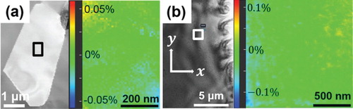
Figure 2. Histograms showing the distribution of strain values from maps recorded from the center of grains in polycrystalline (a) boron carbide and (b) copper. The standard deviations of the data are represented by dashed lines and gray regions. The strain value standard deviations are 0.025% and 0.039% for boron carbide and copper, respectively.
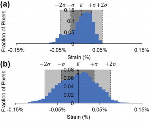
Taking the 95% confidence range as the resolution of the measurement, the strain resolution for boron carbide and copper was determined to be 0.1% and 0.156%, respectively. These values are comparable to the strain resolution of 0.1% commonly reported by others utilizing NBED to study elastic strain in single crystalline silicon [Citation19,Citation29]. The developers of the Topspin automated N-PED technique used in this study were able to obtain a strain resolution of 0.08% for single crystal silicon [Citation24]. For boron carbide, a resolution comparable to single crystalline silicon could be achieved, while the strain resolution for the polycrystalline copper was lower. The poorer resolution is attributable to the retention of defects in the sample after the cold rolling process, annealing, and recrystallization treatment (see Supplemental Material for representative bright-field micrographs of the boron carbide and copper specimens studied here). It is likely that strain resolution for Cu could be improved by studying a specimen with lower concentration of defects. These results confirm that the automated NBED strain mapping technique can be generally applied to a variety of materials systems of engineering significance; however, a defect-free region of material is necessary to establish a strain resolution comparable to what has been observed in single crystal silicon.
With the strain resolution established, the strain field imposed on the materials by various defects can be quantified. shows an orientation map of a boron carbide grain boundary composed of three facets. Each of the facets is inclined differently with respect to the a and c axes of the hexagonal lattice. Both grains are tilted such that they share an a-axis, or , parallel to the electron beam. shows the results of strain maps recorded near this grain boundary with the strain calculated parallel to facets 1, 2, and 3. The average strain parallel to each facet is plotted as a function of distance to the boundary, i.e. from A to B in each map. The dashed box in each strain map represents the pixels across which the strain was averaged. The shaded region represents the 0.1% strain resolution obtained from the center of a grain. The points closest to the boundary are not used in the analysis to avoid spurious strain measurements resulting from superimposed DPs.
Figure 3. Orientation map of boron carbide showing the relative inclination of the a and c axes of grains 1 and 2 with respect to facets 1, 2, 3 using hexagonal wire-frame lattices. In both grains a direction is parallel to the electron beam direction. Since the grains share an out-of-plane orientation, the color of each pixel corresponds to the in-plane orientation to provide contrast between grains.
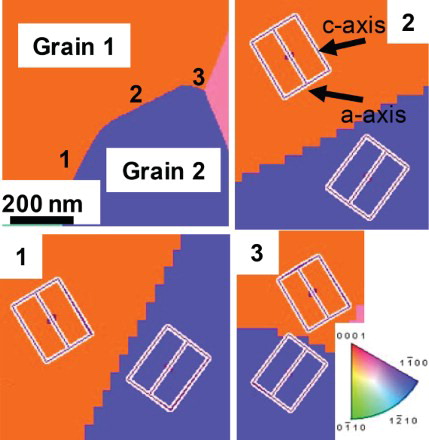
Figure 4. Strain maps (above) and line profiles (below) showing the strain parallel to facets 1, 2, and 3. Strain values are averaged across all pixels parallel to the boundary as indicated by dashed boxes in the strain maps.
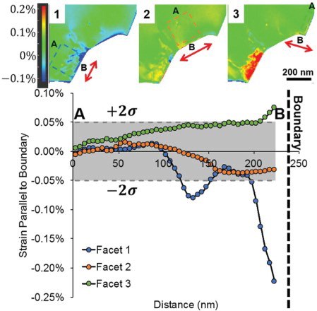
For each facet, the strain measured far from the boundary (>150 nm) is negligible. As the facets are approached, the strain values increase. For facet 1, compressive strain develops and exceeds the threshold set by the strain resolution 120 nm away from the boundary and increases as the boundary is approached to a maximum value of 0.22%. The strain parallel to facet 2 follows a similar pattern, with compressive strains developing parallel to the boundary starting 130 nm away from the boundary. The magnitude of the strain parallel to facet 2 is lower and does not surpass the strain resolution threshold, reaching 0.032% nearest the boundary. The strain parallel to facet 3 is tensile in nature and reaches a maximum value of 0.075% nearest to the boundary. The reference DP along with select DPs near the grain boundary facets used to calculate elastic strain are included in the Supplemental Material.
In order to provide physical meaning to the strains measured parallel to the facets, a simple model was developed to predict the elastic strain that would develop upon cooling of simple boron carbide bicrystals. It is expected that thermal strains will develop upon cooling as a result of the anisotropic coefficient of thermal expansion of boron carbide, in which the length of the c-axis is substantially more sensitive to changes in temperature than the a-axis [Citation30]. Elastic strains arising from thermal anisotropy have been measured in the past for other hexagonal crystal systems, such as Zircaloy-2 [Citation31]. Since grains 1 and 2 share an a-axis nearly parallel to the boundary, strain would only develop according to the in-plane inclination of the c and a axes, as seen in . The researchers in [Citation30] measured the percent thermal expansion of the a and c axes, and
respectively, and from those expressions the effective thermal expansion,
, in a direction inclined an angle
from the a axis can be calculated. Equation (1) gives the effective percent thermal expansion as a function of temperature and
.
(1)
This expression was used to predict the sign of the strain expected to develop parallel to each facet in grain 1 as a result of thermal expansion anisotropy. provides the values of
for each facet of grains 1 and 2 together with the total percent contraction when cooling from
(the temperature above which large scale creep relaxation is known to occur in boron carbide [Citation32]) to room temperature. The rightmost column indicates the sign of the expected strain parallel to each facet in grain 1.
Table 1. Measured θ values and calculated total % contraction values using Equation (1) to determine the sign of the stress parallel to the boundary in Grain 1.
From the table, compressive strains are expected parallel to facets 1 and 2, and tensile strain is expected to develop parallel to facet 3. These predictions correlate very well with the measured strains shown in . A more sophisticated model would be needed to account for anisotropic elasticity and the contribution to strain from other nearby boundaries, estimate the magnitude of expected strain, and to predict the strain in non-parallel directions to the facets. Nevertheless, this example provides the first evidence that strains associated with microstructural defects in polycrystalline ceramics can be directly measured and correlated to expected values using N-PED.
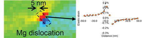
In addition to elastic strains associated with boundaries, elastic strains were measured near individual inclined dislocations and at a low-angle boundary in magnesium. shows a strain map recorded from a polycrystalline Mg specimen that was strained to 1% in tension. The strain is calculated parallel to the c-axis in the map. A TEM foil was prepared using electropolishing and analyzed using N-PED. The specimen was tilted to a direction, or a-axis. The area in the in the strain map contains a low-angle tilt boundary extending from the top-left to bottom-right of the map that is parallel to the beam at this specimen tilt. The tilt across the boundary was determined to be a
rotation about the a-axis parallel to the beam by measuring the rotational difference between DPs on either side of the boundary. The boundary is aligned along the c-axis (indicated by the arrow on the figure) and is composed of basal dislocations. The spacing of the dislocations is close to the step size of the scan (3 nm), making resolution of individual dislocations is difficult. Nevertheless, the average spacing in strain maxima along the boundary was calculated to be 10.4 nm, which corresponds well to the expected spacing of 6.8 nm for edge dislocations with
, as is the case for
or
dislocations in Mg.
Figure 5. Strain map of the region surrounding the low-angle grain boundary in Mg. Strain contrast decorates the low-angle boundary as well as through-thickness dislocations. TEM bright field image from region within triangle is also shown. Strain profiles across two such dislocations are shown on the right. Experimental points are plotted with dashed lines indicating the relation predicted by elastic solutions.
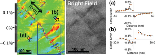
In addition to the dislocations comprising the low-angle boundary, other through-thickness dislocations inclined with respect to the beam direction were observed in the strain map. Strain dipoles were associated with these through-thickness dislocations. Two such dislocations are highlighted in the scan and the strain values across them are plotted in (a) and (b), respectively. Virtual dark field analysis revealed these dislocations to be basal, or a-type dislocations (see Supplemental Material for details). For each dislocation, the magnitude of the measured elastic strain increases as the core is approached and the sign of the strain changes abruptly as the core is passed. These results agree with elastic solutions for the strain field around a single dislocation, which follows a decay away from the core [Citation33]. Equation (2) was used to compare the experimentally measured strain to the elastic strain,
, for the simple case of a screw-type dislocation.
(2)
Where A and C are fitting parameters to account for non-zero baseline strain and centering of the dislocation, respectively; b is the Burgers vector of an
dislocation in Mg,
; and r is the distance from the dislocation core. The elastic solution fits very well at all locations with the exception of the points very close to the dislocation core; this can be attributed to the finite electron probe size that averages the strain value surrounding the dislocation core.
Conclusions
This study provides evidence that elastic strains can be measured and mapped in polycrystalline materials with nanoscale resolution and comparable strain resolution to existing techniques.
Measured strain resolution in maps obtained using automated N-PED for polycrystalline metals and ceramics is comparable to those measured previously for semiconductor materials.
Elastic strain fields near boron carbide grain boundary facets correlate with compressive and tensile strains predicted from thermal contraction anisotropy.
Strain fields associated with single dislocations can be measured using this technique and estimates of dislocation spacing and strain dipoles are in good agreement with predictions.
TMRL_2017_0195.R1_Supplemental_Material.docx
Download MS Word (10.6 MB)Acknowledgements
This work was supported by the U.S. Department of Energy, Office of Science, Basic Energy Sciences, under Award # DE-FG02-07ER46437. Yue Liu of Los Alamos National Laboratory and Richard Haber of Rutgers University are kindly acknowledged for providing specimens and Amith Darbal of AppFive for useful discussion related to N-PED and the AppFive acquision module.
Disclosure statement
No potential conflict of interest was reported by the authors.
ORCID
Paul F. Rottmann http://orcid.org/0000-0001-6718-7402
Additional information
Funding
Related Research Data
References
- Smith CS. Piezoresistance effect in germanium and silicon. Phys Rev. 1954;94:42–49. doi: 10.1103/PhysRev.94.42
- Chidambaram PR, Bowen C, Chakravarthi S, et al. Fundamentals of silicon material properties for successful exploitation of strain engineering in modern CMOS manufacturing. IEEE Trans Electron Devices. 2006;53:944–964. doi: 10.1109/TED.2006.872912
- Withers PJ, Bhadeshia HKDH. Residual stress. Part 1 – measurement techniques. Mater Sci Technol. 2001;17:355–365. doi: 10.1179/026708301101509980
- Bernier JV, Miller MP. A direct method for the determination of the mean orientation-dependent elastic strains and stresses in polycrystalline materials from strain pole figures. J Appl Crystallogr. 2006;39:358–368.
- Miller MP, Park JS, Dawson PR, et al. Measuring and modeling distributions of stress state in deforming polycrystals. Acta Mater. 2008;56:3927–3939. doi: 10.1016/j.actamat.2008.04.062
- Gioacchino FD, da Fonseca JQ. Plastic strain mapping with sub-micron resolution using digital image correlation. Exp Mech. 2013;53:743–754. doi: 10.1007/s11340-012-9685-2
- Tamura N, MacDowell AA, Spolenak R, et al. Scanning X-ray microdiffraction with submicrometer white beam for strain/stress and orientation mapping in thin films. J Synchrotron Radiat. 2003;10:137–143. doi: 10.1107/S0909049502021362
- Choi D, Wang B, Chung S, et al. Phase, grain structure, stress, and resistivity of sputter-deposited tungsten films. J Vac Sci Technol A. 2011;29:051512. doi: 10.1116/1.3622619
- Bierwolf R, Hohenstein M, Phillipp F, et al. Direct measurement of local lattice distortions in strained layer structures by HREM. Ultramicroscopy. 1993;49:273–285. doi: 10.1016/0304-3991(93)90234-O
- Koch CT, Özdöl VB, van Aken PA. An efficient, simple, and precise way to map strain with nanometer resolution in semiconductor devices. Appl Phys Lett. 2010;96:091901. doi: 10.1063/1.3337090
- Müller K, Rosenauer A, Schowalter M, et al. Strain measurement in semiconductor heterostructures by scanning transmission electron microscopy. Microsc Microanal. 2012;18:995–1009. Epub 10/02. doi: 10.1017/S1431927612001274
- Pekin TC, Gammer C, Ciston J, et al. Optimizing disk registration algorithms for nanobeam electron diffraction strain mapping. Ultramicroscopy. 2017;176:170–176. doi: 10.1016/j.ultramic.2016.12.021
- Uesugi F, Hokazono A, Takeno S. Evaluation of two-dimensional strain distribution by STEM/NBD. Ultramicroscopy. 2011;111:995–998. doi: 10.1016/j.ultramic.2011.01.035
- Béché A, Rouvière JL, Clément L, et al. Improved precision in strain measurement using nanobeam electron diffraction. Appl Phys Lett. 2009;95:123114. doi: 10.1063/1.3224886
- Ozdol VB, Gammer C, Jin XG, et al. Strain mapping at nanometer resolution using advanced nano-beam electron diffraction. Appl Phys Lett. 2015;106:253107. doi: 10.1063/1.4922994
- Rouviere J-L, Béché A, Martin Y, et al. Improved strain precision with high spatial resolution using nanobeam precession electron diffraction. Appl Phys Lett. 2013;103:241913. doi: 10.1063/1.4829154
- Mahr C, Müller-Caspary K, Grieb T, et al. Theoretical study of precision and accuracy of strain analysis by nano-beam electron diffraction. Ultramicroscopy. 2015;158:38–48. doi: 10.1016/j.ultramic.2015.06.011
- Reisinger M, Zalesak J, Daniel R, et al. Cross-sectional stress distribution in Alx Ga1−x N heterostructure on Si(111) substrate characterized by ion beam layer removal method and precession electron diffraction. Mater Des. 2016;106:476–481. doi: 10.1016/j.matdes.2016.06.001
- Béché A, Rouvière JL, Barnes JP, et al. Strain measurement at the nanoscale: comparison between convergent beam electron diffraction, nano-beam electron diffraction, high resolution imaging and dark field electron holography. Ultramicroscopy. 2013;131:10–23. doi: 10.1016/j.ultramic.2013.03.014
- Cooper D, Denneulin T, Bernier N, et al. Strain mapping of semiconductor specimens with nm-scale resolution in a transmission electron microscope. Micron. 2016;80:145–165. doi: 10.1016/j.micron.2015.09.001
- Portillo J, Rauch EF, Nicolopoulos S, et al. Precession electron diffraction assisted orientation mapping in the transmission electron microscope. Mater Sci Forum. 2010;644:1–7
- Viladot D, Véron M, Gemmi M, et al. Orientation and phase mapping in the transmission electron microscope using precession-assisted diffraction spot recognition: state-of-the-art results. J Microsc. 2013;252:23–34. doi: 10.1111/jmi.12065
- Rauch EF, Véron M. Automated crystal orientation and phase mapping in TEM. Mater Charact. 2014;98:1–9. doi: 10.1016/j.matchar.2014.08.010
- NanoMEGAS. Topspin automated NBED system. [cited 2017 May]. Available from: http://nanomegasusa.com/strain-mapping/.
- Darbal AD, Narayan RD, Vartuli C, et al. Applications of automated high resolution strain mapping in TEM on the study of strain distribution in MOSFETs. Microsc Microanal. 2014;20:1066–1067. doi: 10.1017/S1431927614007053
- Vigouroux MP, Delaye V, Bernier N, et al. Strain mapping at the nanoscale using precession electron diffraction in transmission electron microscope with off axis camera. Appl Phys Lett. 2014;105:191906. doi: 10.1063/1.4901435
- Xie KY, Kuwelkar K, Haber RA, et al. Microstructural characterization of a commercial hot-pressed boron carbide armor plate. J Am Ceram Soc. 2016;99:2834–2841. doi: 10.1111/jace.14295
- Xie KY, An Q, Sato T, et al. Breaking the icosahedra in boron carbide. Proc Natl Acad Sci USA. 2016;113:12012–6. doi: 10.1073/pnas.1607980113
- Usuda K, Numata T, Takagi S. Strain evaluation of strained-Si layers on SiGe by the nano-beam electron diffraction (NBD) method. Mater Sci Semicond Process. 2005;8:155–159. doi: 10.1016/j.mssp.2004.09.105
- Pilladi TR, Panneerselvam G, Anthonysamy S, et al. Thermal expansion of nanocrystalline boron carbide. Ceram Int. 2012;38:3723–3728. doi: 10.1016/j.ceramint.2012.01.016
- MacEwen SR, Tome C, Faber J. Residual stresses in annealed zircaloy. Acta Metall. 1989;37:979–989. doi: 10.1016/0001-6160(89)90025-4
- Abzianidze TG, Eristavi AM, Shalamberidze SO. Strength and creep in boron carbide (B4C) and aluminum dodecaboride (α-AlB12). J Solid State Chem. 2000;154:191–193. doi: 10.1006/jssc.2000.8834
- Hirth JP, Lothe J. Theory of dislocations. New York: McGraw-Hill; 1968.