
ABSTRACT
A new processing route has been discovered through which far-from-equilibrium, metastable architectures with unprecedented properties are synthesized. This novel architecture contains many orders of hierarchy with multiple concentration modulation wavelengths. At one length scale, the matrix is comprised of lateral modulations of BCC Mo and pseudomorphic BCC Cu with a wavelength of 10 nm. FCC, Cu-rich islands of approximate 250 nm diameter are woven in-between the Mo-Cu matrix and contain ordered arrays of pseudomorphic, FCC, Mo-rich, coherent precipitates of approximately 1.0 nm diameter spacing. The resulting material exhibits unprecedented mechanical behavior of extensive plastic deformability at room temperature.
GRAPHICAL ABSTRACT

IMPACT STATEMENT
Traditional phase separated thin film morphologies are monolithic in architecture with only one concentration wavelength. By carefully manipulating the self-assembly kinetics through the deposition rate, we processed a structure with multiple concentration modulation wavelengths.
1. Introduction
Abrupt changes in the external conditions can force systems into nonequilibrium states. These systems’ kinetic relaxation pathways are often complex and involve phase transitions that may lead to multiple metastable phases. Understanding phase-ordering kinetics is central to controlling the way in which phases organize in a number of material systems [Citation1], particularly in vapor deposited thin films where control of grain [Citation2] or multi-phase [Citation3] morphology is crucial to obtaining novel and enhanced functionalities for technological application [Citation4].
Given the unique governability over the deposition temperature and rate, physical vapor deposition (PVD) has often been the synthesis technique of choice to study phase ordering in immiscible systems [Citation5–8]. Furthermore, unlike bulk phase separation in which the system's bulk thermodynamics dictates the rate of phase separation, PVD allows external control over the rate of separation through the deposition rate, at a given temperature [Citation9]. In this article, we report on a novel PVD synthesis route that dictates dramatic differences in constituent mobilities of Cu and Mo during co-sputtering and results in far-from-equilibrium, metastable, multi-modal architectures during deposition.
Normally, there are two processing routes that can be used to create and study multi-phase morphologies using PVD sputtering: low temperature deposition to produce an amorphous film followed by annealing [Citation10] or depositing at elevated temperature [Citation11]. In the case of the former approach, a binary alloy which is highly immiscible is co-sputtered. Deposition at room temperature results in a chemically homogeneous amorphous film [Citation6]. Annealing the samples at elevated temperature induces phase separation as a result of nucleation and growth or spinodal decomposition depending on the system [Citation12–14]. This generally results in randomly oriented concentration modulations of the two constituents in a bicontinuous morphology if the constituents are of equal phase fraction.
Another processing route involves co-sputtering each immiscible element while heating the substrate. At temperatures high enough to activate phase separation during deposition, constituents self-organize into concentration modulations that are oriented in different directions based upon the deposition conditions [Citation9,Citation11]. The interplay between the rate of phase separation and the rate of deposition determine the final morphology. Laterally, vertically, and randomly oriented concentration modulations have resulted by controlling the substrate temperature. Phase field simulations have confirmed this self-organizing behavior [Citation5].
In both synthesis routes, the resulting morphologies possess a single concentration modulation wavelength with phase separated domains oriented laterally, vertically, and randomly with respect to the substrate [Citation5]. The challenge is to deposit a film with phase separation at multiple length scales forming a hierarchical structure. The current work addresses this challenge by deliberately depositing immiscible constituents, Cu and Mo chosen as the model system, at low deposition rates and high temperatures. The high temperature activates self-assembly via phase separation during deposition as has been shown before, while the low deposition rate creates a large disparity in mobility between the sputtered species assembling on the growing surface.
With differences of orders of magnitude in adatom mobility of the constituents [Citation15,Citation16], heterogeneous structural evolution results in a bimodal architecture with Cu-rich and Mo-rich domains stabilizing at multiple length scales and undergoing further separations within each domain to produce pseudomorphic—or lattice-mismatched metastable phase – crystal structures that do not correspond to the bulk ground state of the constituent elements, namely BCC Cu and FCC Mo. Further, we altered the substrate temperature to coarsen the hierarchical morphology and change the crystal structure of the domains. Finally, we utilize cluster expansion formalism, parameterized with density functional theory (DFT) calculations to investigate the phase stability of metastable Cu and Mo domains given the constraints of the system. Compression tests performed in situ in a transmission electron microscope (TEM) show unprecedented mechanical behavior of extensive plastic deformability at room temperature at flow stress in excess of 2 GPa. This study provides new insights for bottom-up design of nanometallic architectures with high strength and high deformability.
2. Methods
2.1. Materials and deposition
Pure Cu (99.999 %) and Mo (99.95 %) targets were positioned confocally and 5 degrees from normal to a substrate and 180 degrees from each other. A pure Si substrate in the 100 orientation with a micron thick layer of thermal oxide (SiO) was positioned in the middle of a rotating platen (20 rpm) 5 inches from both targets. The base pressure in the chamber prior to deposition was 3.6 E-6 Pa. The substrate was first cleaned using an RF bias of 50 W for 100 s before deposition. The platen was then heated to the desired temperature and held at this temperature for 300 s before deposition. This temperature was maintained throughout the deposition. Both targets were ramped to the target power setting and burned-in for 60 s before deposition. Power at each gun was constant for the duration of the deposition. The Mo target was set to 100 W and the Cu target to 50 W to achieve the same deposition rate for each species. A 45 at.% Cu phase fraction was measured by XRF in the as-deposited film. All of the deposited films were 1 micron in thickness.
2.2. Electron microscopy
Scanning/transmission electron microscopy (S/TEM) foils were prepared using a focused ion beam (FIB) technique in an FEI Helios 650 nanolab SEM/FIB. The foils were attached and thinned on a silicon TEM half grid to prevent any compositional background from the TEM grid. Samples were plasma cleaned for 300 s prior to insertion into the S/TEM. A JEOL 3100R05 double-Cs corrected S/STEM with a point-to-point resolution of 0.055 nm was used to collect HAADF images of the samples. The convergent angle for all image collection was set to 111 degrees at a camera length of 8 cm for true HAADF imaging. Compositional maps were collected using a JEOL SDD X-ray detector with an active area of 60 mm2 capable of detecting elements with Z > 5.
2.3. Nanomechanical testing
Cylindrical nanopillars with diameters of 450 nm and height of 1 μ m were fabricated using FIB in a FEI Helios 650 nanolab SEM. The sample was then mounted onto the stage of a Hysitron PI 95 Picoindenter for in situ testing in TEM. A flat-tip indenter with a 1.5 μ m-diameter end surface was used to conduct the compression test at constant displacement rate with strain rate of −0.2 % s−1. After the test, FIB was used to prepare TEM samples of the deformed pillars for post-mortem characterization. An image of the micropillar before in situ compression is presented in Figure S14.
2.4. DFT calculations
We used the ATAT package [Citation17] to explore the entire composition space, calculating the energies of formation for each configuration, relative to the pure end members, Cu and Mo (in the FCC or BCC states, respectively), through DFT calculations using the VASP software package [Citation18]. All configurations investigated were allowed to completely relax, i.e. volume, shape and atomic coordinates were all allowed to relax to the local equilibrium state. The CE itself was carried out until the error between the predicted energies of formation of arbitrary configurations and those calculated through the DFT code converged approximately within less than approximately 10 meV/spin.
3. Results
3.1. Cu–Mo hierarchical structure and characterization
The morphology, including chemistry and crystal structure, of a co-deposited Cu–Mo film at relatively low deposition rate is shown in Figure . The synthesis procedures can be found in the Supplementary Figure S1. In HAADF phase contrast imaging, it was observed that these samples exhibited morphological features on at least two different length scales.
Figure 1. High-angle annular dark-field scanning transmission electron microscopy (HAADF-STEM) images taken along the direction of FCC Cu. The high-level view of the sample in (a) displays the hierarchical structure of the sample throughout the thickness and length of the film. Direction of growth is from bottom to top in the image. Scale bar, 1 micron. At one length scale in (b-d), the single crystal Cu grains contain FCC Mo dispersoids arranged in an FCC superlattice as indicated in the power spectrum (c) taken from (d); indexed down the FCC
zone axis. The energy dispersive X-ray spectrum map in (b) shows a concentration of Mo corresponding to the brighter spots in the STEM image. Scale bars, 1 nm (b), 10 nm (d). Another length scale is presented in (e–f) where Cu and Mo are constrained to a coherent BCC Mo-Cu solid solution and exhibit lateral concentration modulations with respect to the film-substrate interface. (e) shows an SADP from the bicontinuous region and only BCC Mo frequencies are present, but Cu–Mo concentration modulations are observed in the EDXS mapping in (f). Scale bar, 50 nm.
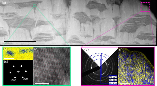
At low magnification, relatively large Cu-rich domains in the darker contrast of approximately 100 nm in lateral and vertical dimension were interspersed in a Cu–Mo bicontinuous matrix. These faceted Cu-rich domains were homogeneously distributed through and across the thickness of the film as shown. The chemical composition of these domains were approximately 95 at.% Cu as measured by EDXS. The bicontinuous matrix maintained an approximate 45 at.% Cu composition as measured by EDXS and thus, Cu species were not removed from the matrix to form these large Cu-rich domains and abnormal grain growth can be ruled out as a cause of this growth, even though Cu in this structure has a mobility advantage compared to Mo [Citation15,Citation16]. The origin of these large Cu-rich domains is instead from a modified Volmer-Weber thin film growth mechanism. In the Volmer-Weber growth mode, the adatom cohesion is stronger than surface adhesion and forms 3D adatom cluster or islands [Citation19]. The dramatic difference in mobility of Cu compared to Mo leads to in homogeneous agglomeration in the growing film as the more mobile Cu readily coalescences compared to the Mo, which lags behind in surrounding, smaller clusters.
Probing the large Cu-rich domains in HAADF imaging at high magnification showed that these islands exhibited the bulk ground state crystal structure of FCC Cu. However, regions of periodically distributed Mo nano-particles were observed throughout each of the Cu-rich grains. Figure (b) shows an EDXS mapping of the Cu-rich matrix in yellow and agglomerations of Mo-rich particles in an ordered FCC superlattice arrangement. FFT analysis shown in Figure (c) taken from the high magnification HAADF image in Figure (d) shows bulk FCC Cu frequencies in the <110> direction. Interestingly, FCC Mo spots are present in the FFT pattern as well, but tightly surrounding the center spot. These are frequencies from the ordered Mo nanoparticles within the Cu-rich matrix encircled in Figure (d).
Previsouly, Mo has only been found to exist in an FCC state under high pressures [Citation20]. However, our DFT-parameterized cluster expansion calculations described below have shown that the FCC Mo does have a low energy metastable state at compositions close to the Mo-end of the composition rage, which is consistent with what we observe here. In the Supplementary Materials section, it is shown how other Cu-refractory metal pairs exhibit an analogous behavior. The ordered arrangement of Mo particles formed an FCC superlattice within the Cu-rich domains. This superlattice is not unlike those found in ultra-thin metallic multilayers and quantum dots [Citation21,Citation22]. In our case, insufficient mobility in the Mo atoms results in them becoming ‘trapped’ within the Cu-rich domains, preventing their agglomeration into larger precipitates. Critical accumulation of Cu leads to island nucleation and growth whereas regions with slightly less Cu and more Mo phase-separate into lateral concentration modulations.
At a larger length scale, the matrix surrounding the Cu-rich domains was observed to have a bicontinuous morphology with lateral Cu-rich and Mo-rich sheets extending from the substrate to the top surface of the film. The selected area diffraction pattern (SADP) shown in Figure (e) only shows frequencies from the BCC Mo crystal structure. EDXS analysis of the matrix shows the presence of Cu-rich and Mo-rich domains with a lateral morphology that extend into the thickness of the film as sheets. High-resolution imaging of the bicontinuous matrix shows a coherent structure where Cu has stabilized into a metastable BCC Cu crystal structure and taken on the BCC Mo lattice parameter. A high magnification image of these Cu and Mo-rich domains can be accessed in Supplementary Figure S2. This has been shown before in Ti/Al [Citation23], Cu/Nb [Citation24], and Mg/Nb [Citation25,Citation26] multilayers where absolute length scale of the structure and the relative thickness of the individual layers have given rise to metastable structures. A plan-view image of the sample is shown in Supplementary Figure S3. This ordered structure has been discovered before in our work on Cu–Mo [Citation11] and other reports on Al–Si systems [Citation8], where the rate of deposition is slower than the rate of phase separation of the growing surface. This difference in rates allows for the formation of a phase separated template where each domain is at its terminal composition and subsequently deposited layers diffuse to like domains underneath [Citation8,Citation11].
3.2. Equilibrium structures at higher deposition temperatures
Coarsening of the structures at all lengths scales was observed when Cu and Mo was deposited at higher substrate temperatures. At 600C, as shown in Figure (a), the Cu-rich domains have expanded to approximately 200 nm in both the lateral and horizontal dimension. The spacing between the Cu-rich domains has also increased. As shown in Supplementary Figure S3, the frequency of observable, periodic FCC Mo particle domains also increased. The most striking morphology change was the lateral concentration modulations that comprised the matrix. The chemical separation of the Cu- and Mo- rich domains was maintained at the higher temperature as compared to the sample deposited at 400
C, but the two-fold increase in length scale in the Cu-rich domains no longer support a coherent BCC Mo, BCC Cu crystal structure. Instead, the Cu-rich domains have crystallographically transformed into their bulk FCC Cu phase as shown in (b). The interface was observed as semi-coherent with the Kurdjumov–Sachs orientation relationship, Cu(111)//Mo(110) and Cu<110>//Mo<111>. This is similar to Cu/Nb multilayers although oriented 90 degrees in relation to the substrate/film interface [Citation5]. A plan-view image of this sample is shown in Supplementary Figure S3.
Figure 2. HAADF-STEM image of a Cu–Mo film under the same conditions as in Figure , but deposited at 600C. The sample exhibits coarsening of all features and the phase separated matrix exists as BCC Mo and FCC Cu. Scale bar, 200 nm. (b) A highly magnified HAADF image showing the Cu–Mo interface in the bicontinuous region. A K–S orientation relationship was present. Scale bar, 1 nm. (c) At a substrate temperature of 700
C further coarsening was observed and the larger Cu grains still contain FCC Mo particles, but each particle is much larger and are no longer arranged periodically. One of these particles is magnified in high resolution in (d) with the corresponding FCC [011] FFT pattern in the inset. Scale bar, 10 nm. For a Cu–Mo sample deposited at 800
C as shown in (e), the features are again coarser. Only coarser BCC Mo particles were present in the Cu grains, one of which is shown in (f). Scale bar, 10 nm.
![Figure 2. HAADF-STEM image of a Cu–Mo film under the same conditions as in Figure 1, but deposited at 600C. The sample exhibits coarsening of all features and the phase separated matrix exists as BCC Mo and FCC Cu. Scale bar, 200 nm. (b) A highly magnified HAADF image showing the Cu–Mo interface in the bicontinuous region. A K–S orientation relationship was present. Scale bar, 1 nm. (c) At a substrate temperature of 700C further coarsening was observed and the larger Cu grains still contain FCC Mo particles, but each particle is much larger and are no longer arranged periodically. One of these particles is magnified in high resolution in (d) with the corresponding FCC [011] FFT pattern in the inset. Scale bar, 10 nm. For a Cu–Mo sample deposited at 800C as shown in (e), the features are again coarser. Only coarser BCC Mo particles were present in the Cu grains, one of which is shown in (f). Scale bar, 10 nm.](/cms/asset/c748f98c-028e-4a85-a8f4-ae3ed3a6d990/tmrl_a_1546237_f0002_oc.jpg)
At 700C, further coarsening was observed as seen in Figure (c). Interestingly, the periodicity of the FCC Mo particles was no longer observed. Rather, larger FCC Mo domains were found throughout the Cu-rich islands as if the Mo domains observed at lower substrate temperatures have coalesced as shown in Figure (d). Even at the higher substrate temperature and larger size, the crystal structure of the Mo domains are still in the metastable FCC phase.
However, another crystallographic transformation occurred for the Mo particles at 800C as shown in Figure (e) and (d). For substrate temperatures up to 700
C, the Mo particles varied in size but maintained the metastable FCC crystal structure. There was a small density of equilibrium BCC Mo at this temperature. It was observed that only Mo particles above 8 nm were in the BCC phase. At 800
C, most of the Mo agglomerates existed as larger particles, and have fully formed into the bulk BCC Mo state. The density of FCC vs. BCC Mo particle size and density are plotted in Figure S9. To obtain the density we measured the thickness of the TEM foil using EELS and then counted the number of particles in a given image with certain X and Y dimensions. We measured no BCC Mo in the Cu grains until 700
C. The density of BCC Mo was still very small compared to the FCC Mo even at at this temperature. At 800
C, the density of stable BCC Mo particles increase dramatically. The size of each Mo structural polymorph trended linearly with increasing deposition temperature. As aforementioned, the size of the BCC Mo particles were no smaller than approximately 5 nm. This is much larger than the approximately 1 nm FCC Mo particles. In future experimentation, we will look to annealing the structure deposited at 400
C to further study the Mo particle transition inside the large Cu grains.
3.3. High strength material without shear banding after compression
The mechanical properties of this hierarchical structure are of particular interest to us because they provide a platform to study heterogeneous materials which have domains that are expected to be softer (the Cu-rich islands) and matrices that are expected to be exceptionally strong (Cu/Mo nanocomposite).
The structure studied here is comprised of Cu and Mo at two length scales: an interpenetrating 5 nm BCC Cu and 5 nm BCC Mo matrix; and 200 nm FCC Cu-rich domains containing FCC Mo nanoparticles that are approximately 1 nm in size. The stress–strain response of the hierarchical structure was investigated using nanopillar compression tests. Figure shows a true stress–strain curve obtained by this technique. Appreciable strain hardening can be observed until a maximum stress of 2.3 GPa was obtained at 12% plastic strain. Directly under the indent it was observed that the thickness of both Cu and Mo LCM domains increased to 7 nm. Further away from the indent tip, the LCM domains were reduced to 1.5 nm in length. The shape of the laminates was also altered to conform to the shape of the indent tip. The enhanced plastic deformation of this structure without shear banding is accounted for by the large Cu domains. The plasticity begins in the lower strength Cu domains, but the distributed Mo particles in these Cu grains increase the strength of the composite as a result of precipitate hardening. As can be seen in the in-situ TEM compression tests presented in Figure , while the Cu domains are strain hardening, the bicontinuous Cu/Mo region begins to plastically deform. As elucidated in [Citation27], the absence of shear banding is a result of the Cu grains diverting once a shear band encounters the Cu domains. In the bicontinuous region, the tortuousness of the interfaces make the glide of a dislocation difficult and thus limiting flow localization. Further high resolution in-situ TEM testing is required to confirm what happens to the Mo particles during deformation. An image of the micropillar before in situ compression is presented in Figure S14.
Figure 3. (a) True stress–true strain curves measured from nanopillar compression tests of the hierarchical structure (blue line and image (c)) and a 3 nm Cu/Mo multilayer (red line and image (b)). (b) STEM image of a 3 nm Cu / 3 nm Mo multilayer nanopillar after the compression test. (c) STEM image of a nanopillar made from the Cu/Mo hierarchical structure deposited at 400C after a compression test. (d) Magnified image of sample shown in (c) showing no plastic flow localization in the Cu/Mo LCM matrix. (a–c) Scale bar, 200 nm. (d) Scale bar, 50 nm.
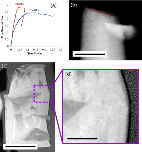
In contrast, the red curve in Figure a shows data measured from a Cu/Mo multilayer with an individual layer thickness of 3 nm. A strain burst and stress drop were observed immediately after yielding. The lack of plasticity in the multilayer can be ascribed to localized shearing. A STEM image of the multilayered pillar after compression can be found in Figure (b), where the top corner of the pillar completely sheared along the dotted line. Figure (c) shows the nanopillar of the hierarchical structure after compression. The pillar remained intact with the deformation distributed throughout the thickness of the whole sample. A significant amount of strain came from the deformation of Cu rich islands, which is evidenced by the extrusions circled in Figure (c). Because of the Cu island has access to the free surface of the nanopillar, the 2.3 GPa stress is an underestimate of the strength of the bulk material. With Cu rich islands fully constrained by the fine scale matrix, the stress level that can be sustained is expected to be higher. However 2.3 GPa is already comparatively high, close to the 2.8 GPa maximum flow stress measured in the 3 nm multilayer, which is the highest stress value reported from a Cu/Mo based metallic material [Citation27,Citation28]. Gradual strain softening was observed in the hierarchical nanopillar after the peak stress. The stress remained above 2 GPa up to 20% plastic strain and no catastrophic failure was observed when the test stopped at 22% plastic strain. Figure (d) shows a magnified image of the region in the rectangle in Figure (c), where the matrix underwent highest amount of deformation. Shear band like those observed in Cu-refractory metal multilayers were not evident in the region [Citation27,Citation29,Citation30]. Our hierarchical Cu/Mo structures thus provides high strength and sustainable plasticity with suppressed shear band formation.
It has been reported in previous works [Citation20] that shear deformation will cause a structural transformation in BCC Mo. Mo will transform into FCC under significant pressure (≈ 8 GPa) even at room temperature. In this work, structural transformations from BCC Mo to FCC Mo as a result of our nanopillar compression tests were not observed post-mortem. While further study is needed to confirm this by completing in-situ compression tests, the required shear stress was not applied during the nanomechanical testing in this work. Further experimentation will be conducted to confirm any potential phase transformations in FCC Mo particles.
It has been reported in previous works (Wang, 2014) that shear deformation will cause a structural transformation in BCC Mo. Mo will transform into FCC under significant pressure (8 GPa) even at room temperature. In this work, structural transformations from BCC Mo to FCC Mo as a result of our nanopillar compression tests were not observed post-mortem. While further study is needed to confirm this by completing in-situ compression tests, the required shear stress was not applied during the nanomechanical testing in this work.
Local stresses and strains where the localized deformation was observed were not determined in this work. This will need to be studied using crystal elastic-plastic and FEM models in future work. Additionally, micropillar compression tests on larger samples (not just in situ TEM) as well as tensile and bend tests will be reported in future reports.
3.4. DFT calculations of Cu–Mo phase stability
We used the cluster expansion (CE) formalism [Citation17,Citation31,Citation32] to parameterize the energetics of FCC- and BCC-based lattice alloys between Cu and Mo (as well as other Cu-refractory element pairs, as reported in supplementary information). Formally, a CE is defined by assigning occupation variables (with integer values), , to each site I of a lattice that has configurational degrees of freedom, i.e. where more than one species can occupy a lattice site. Using this framework, we proceeded to explore the ground state of the FCC and BCC Cu–Mo systems by systematically enumerating different occupancy configurations within an underlying FCC/BCC motif. Figure shows the results of these investigations.
Figure 4. (a) Plots of the energy per spin in meV versus the mole fraction of Mo (x) in a Cu–Mo FCC system in the ground state.The calculations suggested a high exothermic state at compositions close to x = 5/6 = 0.83. (b) shows the same calculations for a Cu–Mo BCC system where immiscibility is preferred.
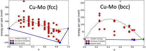
Figure is notable in many respects. First of all, our investigation of the ground state in the case of the FCC Cu–Mo system suggests, contrary to expectations based on the observed bulk phase diagram in the Cu–Mo system, that Cu and Mo are actually miscible when the system is restricted to exist in the FCC state throughout the entire composition range. More specifically, the calculations show that the system undergoes a transition from endothermic to exothermic mixing as the system becomes richer in Mo. The calculations even suggest a high exothermic state at compositions close to x = 5/6 = 0.83333. At this composition, the system undergoes a LRO transformation and the ordered compound has an energy of formation relative to pure Cu and Mo in the FCC state of −200 meV/spin or close to −20 kJ/mol-atom. In the case of the BCC Cu–Mo system, on the other hand, the calculated energies of formation for configurations across the entire composition range suggest instead a tendency towards immiscibility, with a maximum energy of mixing of approximately +150 meV/spin or +15 kj/mol-atom. Notably, in this case there are configurations that exhibit ideal mixing (and to some degree exothermic tendencies) at compositions close to x = 5/6 = 0.83333.
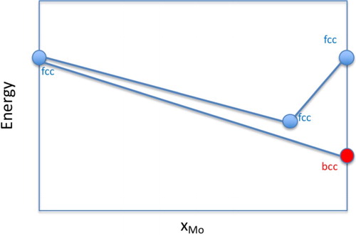
These results are remarkable in that in neither case any type of constraint was imposed on the system, other than preserving the underlying FCC/BCC lattice. Each configuration, as stated above, was allowed to relax towards a (local) equilibrium, so the stabilization of a highly exothermic configuration in FCC Cu–Mo at x = 0.83333 cannot be ascribed to coherency constraints of any kind. Liu and Zunger [Citation33,Citation34] have shown how such constraints can lead to ordering in systems intrinsically immiscible in the bulk but in this specific case. Thus, contrary to what one might infer from the bulk phase diagram, Cu and Mo are at least partially miscible in the FCC state. The question then arises as to the reason for the observed immiscibility in the phase diagram. While a full phase stability analysis is beyond the scope of this work, the most likely explanation is the fact that the BCC-Mo state is very stable and the most stable tie-line between the Cu- and Mo-rich phases in this system are shared by a Cu-FCC and a Mo-BCC state, as shown schematically in Figure .
Figure 5. Schematic of phase stability competition between the FCC and BCC states in the Cu–Mo system.
To rule out any systematic issue with the calculated energetics for this system, we proceeded to investigate the alloying behavior in other Cu-refractory metal (RM) systems ( Cu–Nb, Cu–Ta, and Cu–W) in the FCC state. As can be seen in Supplementary Figure S4, in all of these systems, similar asymmetric trends in which the system goes from immiscible to miscible as the amount of RM increases can be observed. Any systematic error in the DFT calculations or the CE-based search are thus ruled out. Interestingly, these results are somewhat corroborated by recent investigations in the Cu–V multi-layered system [Citation35]. In this system, Guo and coworkers investigated the evolution of growth stresses and interfacial structure in Cu–V multi-layered thin films and found that when the individual layers had thicknesses less than 0.5 nm considerable intermixing was present. In their films, due to the considerably higher stiffness of V relative to Cu the BCC Cu state was stabilized. The explanation for the observed intermixing in the Cu–V case was ascribed to a surface exchange mechanism that resulted from the system attempting to minimize the interfacial energy between individual Cu and V layers. These results, however, suggest that an intrinsic thermodynamic tendency towards mixing may be prevalent in these systems.
For completeness, and to gain a better sense of the significance of the results presented above, we proceeded to calculate the ground state for the Cu–Ni FCC system, as shown in Supplementary Figure S5, using the same CE-based framework as before. In this case, it is shown that the system exhibits a small degree of immiscibility (of less than 2.5 kJ/mol-atom) although there are a large number of configurations lying on the Cu–Ni ground state. Cu–Ni form a prototypical isomorphous phase diagram at finite temperatures but the fact that it exhibits some degree towards phase separation is a consequence of the Third Law as at low temperatures, when entropic contributions are vanishingly small, systems either order or phase separate.
4. Discussion
We have demonstrated that nominally immiscible Cu–Mo mixtures are able to self-organize into surprisingly rich, hierarchical structures. Our DFT calculations show that there are thermodynamic factors favoring such self-organization. However, understanding why these structures only form within a specific window of deposition rates and temperatures calls for an analysis of the kinetics of their formation. Phase separation during thin film growth has been shown to occur only on the exposed free surface because the surface interdiffusion rates, temperatures, and deposition times are too small to allow for significant diffusion in the bulk in many systems, including Al–Ge and Cu–Mo [Citation7,Citation13]. This situation has been named the ”frozen bulk approximation” by Adams et al [Citation9]. In it, the morphology of the film below the surface is a record of the history of the surface composition profile in systems that phase separate during deposition. This means that depth into the film is equivalent to time [Citation9]. Since thin film organization is strictly confined to the growing surface, any net vacancy flux required by Darken's analysis may be accommodated by changes in surface topography [Citation36]. This is consistent with our observation of mounds that developed on the surfaces of the hierarchical structures as shown in Figure S8.
Previously, the frozen bulk approximately has only been used to analyze homogeneously distributed concentration modulations with a single bilayer wavelength. To adapt this assumption to the morphology observed in our work, we combine it with a modified Volmer-Weber growth mechanism that results in large Cu domains distributed throughout the film. The inhomogeneity in crystal structure, chemical composition, and morphology in the Cu–Mo hierarchical films studied here is a result of large differences in surface diffusion rates of the constituents combined with a low deposition rate. The sluggish diffusion of Mo atoms or clusters moving on the surface of the film is an order of magnitude smaller than the measured surface mobility of Cu [Citation15,Citation16]. The frozen bulk approximation restricts atoms to only diffusing on the growing surface and the dissimilarity in surface diffusion rates leads to the Cu-rich and Mo-rich domains found on multiple length scales that were observed in this structure. A cartoon schematic in Figure S6 shows the growth progression.
In Figure S6, the first layer to arrive on the surface of the substrate is composed of an approximately equal phase fraction of Cu and Mo constituents. Phase decomposition begins as atoms begin to to wet the surface and like-atoms attempt to aggregate in like-domains as described by Wang and colleagues [Citation5]. Before the next layer of material arrives on the surface, the faster Cu species diffuse on the surface and agglomerate much more readily than Mo and form Cu-rich domains.
At the next time step in Figure S6, the subsequent few layers of material have arrived to form a complete monolayer of material. The Cu domains have enlarged while the Mo-rich domains have also grown in size but at a slower rate and are left in-between the Cu domains. Cu atoms that have not yet reached the large Cu-domains are buried in between the Mo domains beginning the template for the lateral concentration modulated matrix. This first complete layer of material forms a template or seed for subsequent depositing atoms. During the rest of the deposition, the Cu and Mo atoms simply follow this template formed at the start of the films and develop a hierarchical structure.
A calculation of the surface diffusion length for Cu and Mo species is plotted in Figure S7. We simply used the diffusion length equation, Equation (Equation1(1) )
(1) where D is the surface diffusivity of Cu, t is the average time to deposit a monolayer, and d is the approximate spacing between the large Cu islands, to compute the surface diffusion length and compare this to the approximate spacing of the Cu ‘islands.’ In the associated plot, at each of the deposition temperatures exposed to the constituents during sputtering—473, 673, and 873 K—the Cu atoms are allowed to diffusion to greater distances than the average spacing between large Cu domains. This is unlike Mo, where at each of the deposition temperatures, the Mo species cannot diffuse long enough to agglomerate as the Cu atoms do.
Previous work on the Cu–Mo system done at much higher deposition rates (0.7 nm/s) for each constituent does not exhibit hierarchical morphologies containing large Cu domains [Citation11]. In this case, the higher deposition rates means that the growing surface is buried and frozen in place much faster. As such, there is not enough time for Cu atoms to agglomerate before being buried by the subsequent layer and the difference in mobility between the constituents is negligible, forming homogeneously distributed Cu/Mo concentration modulations.
The modified Volmer-Weber growth process proposed here does not explain several aspects of the the hierarchical structure we observed, calling for further investigation. Examples include the pseudomorphic Mo precipitate lattice contained within the Cu domains, the observation that the large Cu domains eventually stop growing (i.e. do not form columns), and that lateral domains of Cu/Mo eventually form atop the Cu domains. The topics will be addressed in future studies.
In summary, we have synthesized a novel, pseudomorphic Cu–Mo hierarchical thin film with differing structure on multiple length scales. Cu and Mo constituents are chemically separated in the structure, but exist in metastable crystal structures at different locations within the film. These metastable states rationalized via DFT calculations. At low temperatures, the matrix is comprised of coherent BCC Cu–Mo lateral concentration modulations and large Cu-rich domains with ordered FCC Mo particles are scattered throughout the film. At higher temperatures, the structure on all length scales coarsens and the metastable Cu and Mo domains relax towards their bulk crystal structures. This structure proved to be both strong and plastically deformable in compression.
Disclosure statement
No potential conflict of interest was reported by the authors.
ORCID
Raymundo Arróyave http://orcid.org/0000-0001-7548-8686
Additional information
Funding
References
- Alert R, Tierno P, Casademunt J. Formation of metastable phases by spinodal decomposition. Nat Commun. 2016;7:1–7. doi: 10.1038/ncomms13067
- Thompson CV. Structure evolution during processing of polycrystalline films. Ann Rev Mater Sci. 2000;30(1):159–190. doi: 10.1146/annurev.matsci.30.1.159
- Nan C-W, Jia Q. Obtaining ultimate functionalities in nanocomposites: design, control, and fabrication. MRS Bull. 2015;40(9):719–724. doi: 10.1557/mrs.2015.196
- Nix WD. Metallic thin films: stresses and mechanical properties. In: Barmak K and Coffey K, editors. Metallic films for electronic, optical and magnetic applications, Woodhead; 2014. p. 353–421.
- Lu Y, Wang C, Gao Y, et al. Microstructure map for self-organized phase separation during film deposition. Phys Rev Lett. 2012;109(8):1–5. doi: 10.1103/PhysRevLett.109.086101
- Müller CM, Sologubenko AS, Gerstl SSA, et al. On spinodal decomposition in Cu–34at.% Ta thin films An atom probe tomography and transmission electron microscopy study. Acta Mater. 2015;89:181–192. doi: 10.1016/j.actamat.2015.01.073
- Adams CD, Atzmon M, Cheng Y-T, et al. Phase separation during co-deposition of AlGe thin films. J Mater Res. 1991;7(03):653–666. doi: 10.1557/JMR.1992.0653
- Fukutani K, Tanji K, Saito T, Den T. Phase-separated Al-Si thin films. J Appl Phys. 2005;98(3):033507. doi: 10.1063/1.1994942
- Adams CD, Srolovitz DJ, Atzmon M. Monte Carlo simulation of phase separation during thin-film codeposition. J Appl Phys. 1993;74(May 2008):1707–1715. doi: 10.1063/1.354825
- Müller CM, Spolenak R. An in situ X-ray diffraction study of phase separation in CuTa alloy thin films. Thin Solid Films. 2016;598:276–288. doi: 10.1016/j.tsf.2015.12.028
- Derby B, Cui Y, Baldwin JK, et al. Effects of substrate temperature and deposition rate on the phase separated morphology of co-sputtered, Cu-Mo thin films. Thin Solid Films. 2018;647(December 2017):50–56. doi: 10.1016/j.tsf.2017.12.013
- Gržeta B, Radić N, Gracin D, et al. Crystallization of Cu50W50 and Cu66W34 amorphous alloys. J Non Cryst Solids. 1994;170(1):101–104. doi: 10.1016/0022-3093(94)90109-0
- Puthucode A, Kaufman MJ, Banerjee R. Early stages of crystallization in phase-separated amorphous copper-niobium alloy thin films. Metallogr Mater Trans A. 2008;39(7):1578–1584. doi: 10.1007/s11661-007-9337-9
- Zhang Z, Guo J, Dehm G, Pippan R. In-situ tracking the structural and chemical evolution of nanostructured CuCr alloys. Acta Mater. 2017;138:42–51. doi: 10.1016/j.actamat.2017.07.039
- Steigman J, Shockley W, Nix FC. The self-diffusion of copper. Phys Rev. 1939 Jul;56:13–21. doi: 10.1103/PhysRev.56.13
- Askill J, Tomlin DH. Self-diffusion in molybdenum. Philos Mag. 1963;8(90):997–1001. doi: 10.1080/14786436308214459
- van de Walle A, Asta M, Ceder G. The alloy theoretic automated toolkit: a user guide. Calphad. 2002;26(4):539–553. doi: 10.1016/S0364-5916(02)80006-2
- Jürgen H. Ab-initio simulations of materials using VASP: density-functional theory and beyond. J Comput Chem. 2005;29(13):2044–2078.
- Oura K., Lifshits V. G., Saranin A., et al. Surface Science: An Introduction. Berlin-Heidelberg, Germany: Springer-Verlag; 2010.
- Wang SJ, Wang H, Du K, et al. Deformation-induced structural transition in body-centred cubic molybdenum. Nat Commun. 2014 Mar;5:3433. doi: 10.1038/ncomms4433
- Parkin SSP, More N, Roche KP. Oscillations in exchange coupling and magnetoresistance in metallic superlattice structures: co/ru, co/cr, and fe/cr. Phys Rev Lett. 1990 May;64:2304–2307. doi: 10.1103/PhysRevLett.64.2304
- Redl FX, Cho K-S, Murray CB, et al. Three-dimensional binary superlattices of magnetic nanocrystals and semiconductor quantum dots. Nature. 2003 Jun;423(6943):968–71. Copyright - Copyright Macmillan Journals Ltd. Jun 26, 2003; Last updated - 2017-10-31; CODEN - NATUAS. doi: 10.1038/nature01702
- Shechtman D, van Heerden D, Josell D. FCC titanium in Ti-Al multilayers. Mater Lett. 1994;20(5):329–334. doi: 10.1016/0167-577X(94)90039-6
- Anderson PM, Bingert JF, Misra A, et al. Rolling textures in nanoscale Cu/Nb multilayers. Acta Mater. 2003;51(20):6059–6075. doi: 10.1016/S1359-6454(03)00428-2
- Ham B, Zhang X. High strength Mg/Nb nanolayer composites. Mater Sci Eng. 2011;528(4):2028–2033. doi: 10.1016/j.msea.2010.10.101
- Junkaew A, Ham B, Zhang X, et al. Stabilization of bcc Mg in thin films at ambient pressure: experimental evidence and ab initio calculations. Mater Res Lett. 2013;1(3):161–167. doi: 10.1080/21663831.2013.804218
- Cui Y, Derby B, Li N, et al. Suppression of shear banding in high-strength Cu/Mo nanocomposites with hierarchical bicontinuous intertwined structures. Mater Res Lett. 2018;6(3):184–190. doi: 10.1080/21663831.2018.1431315
- Zhang X, Hundley MF, Malinowski A, et al. Microstructure and electronic properties of Cu/Mo multilayers and three-dimensional arrays of nanocrystalline Cu precipitates embedded in a Mo matrix. J Appl Phys. 2004;95(7):3644–3648. doi: 10.1063/1.1649795
- Mara NA, Bhattacharyya D, Dickerson P, et al. Deformability of ultrahigh strength 5nm CuNb nanolayered composites. Appl Phys Lett. 2008;92(23):231901. doi: 10.1063/1.2938921
- Misra A, Kung H, Hammon D, et al. Damage mechanisms in nanolayered metallic composites. Int J Damage Mech. 2003;12(4):365–376. doi: 10.1177/105678903036227
- Kresse G, Furthm”uller J. Efficient iterative schemes for ab initio total-energy calculations using a plane-wave basis set. Phys Rev B. 1996 Oct;54:11169–11186. doi: 10.1103/PhysRevB.54.11169
- Kresse G, Furthmüller J. Efficiency of ab-initio total energy calculations for metals and semiconductors using a plane-wave basis set. Comput Mater Sci. 1996;6(1):15–50. doi: 10.1016/0927-0256(96)00008-0
- Liu JZ, Zunger A. Thermodynamic states and phase diagrams for bulk-incoherent, bulk-coherent, and epitaxially-coherent semiconductor alloys: application to cubic (ga,in)n. Phys Rev B. 2008 May;77:205201.
- Liu JZ, Zunger A. Thermodynamic theory of epitaxial alloys: first-principles mixed-basis cluster expansion of (In, Ga)N alloy film. J Phys. 2009;21(29):295402.
- Zeng LF, Gao R, Xie ZM, et al. Development of interface-dominant bulk Cu/V nanolamellar composites by cross accumulative roll bonding. Sci Rep. 2017 Dec;7(2016):1–9.
- Balluffi RW, Allen SM, Carter WC, et al. Kinetics of Materials. Hoboken, NJ, USA: John Wiley & Sons; 2005.