
Abstract
We streamlined a way towards first experimental demonstration of synthesizing one-dimensional Co–Cu–Fe–Ni–Zn high-entropy alloy (HEA) nanowires (NWs) by an economical electrochemical technique in aqueous medium. HEA NWs have a face-centred cubic structure with nanocrystalline features, including twins along the nanowire of uniform length ∼50 µm and diameter 100 ± 20 nm. Control over the formation and uniform stoichiometry (required range for HEAs ∼ 5–35 atom %) throughout the HEA NWs and its nanocrystallinity was achieved using pulse electrodeposition. These Co–Cu–Fe–Ni–Zn nanowires are a new family of HEAs containing both magnetic and non-magnetic elements in addition to its new 1D morphology.
GRAPHICAL ABSTRACT
IMPACT STATEMENT
A breakthrough in attaining single FCC phase high-entropy alloy nanowires through aqueous electrochemical route which facilitates new possibilities for unexplored applications of high-entropy alloys at lower dimensions.
Introduction
Unique one-dimesional (1D) morphology like nanowires of pure metals, alloys and their oxides, sulphides, nitrides have become imperative in electronics [Citation1,Citation2] such as transistors, quantum devices, nanosensors, etc. In addition, due to their exceptional functionalities through a wide concentration range, they are being used in several device applications such as in energy [Citation3] and biomedicine [Citation4]. On the other hand, studies reported on metallic nanowires are restricted to a very small compositional space not exceedingly more than three to four elements [Citation5,Citation6]. Furthermore, the current evolution of new high-entropy alloys with remarkable performance has opened the possibilities of exploring enormous combination of unfamiliar alloys in bulk [Citation7–9]. Recently, new initiatives have been taken in downsizing these HEAs into thin films [Citation10] and nanoparticles [Citation11] but not towards other new morphologies. In addition, there are very limited HEA families that have been investigated by conventional methods of synthesis due to complexities in mixing of multiple elements in a large compositional space [Citation12,Citation13]. Therefore, a demand to develop a new combination of alloys is still high, preferably high-entropy alloys with various morphologies having unprecedented functionalities which would contribute to a significant advancement for the next-generation materials. In anticipation, a few attempts have been made on multicomponent oxides by dealloying [Citation14]; however, there is no investigation found on HEA NWs especially on a new alloy system in a single step.
With the inclination on fabricating nanowires, very few approaches have been preferred such as chemical methods [Citation15–17], lithography [Citation18], printing [Citation19] etc. Moreover, several aspects, such as chemical stability, crystallinity, and composition of the HEA NWs, must be taken into consideration, while nominating a suitable technique among the numerous available methods [Citation20–22]. Out of the existing methods, the available electrochemical approach is conterminous for synthesizing nanowires [Citation22,Citation23] and it is recently being used in synthesizing multicomponent alloy thin films. In this regard, template-assisted electrochemical approach has several advantages such as simplicity of operation, low cost, ease of availability, reliability and scalability with a new combination of concentrated elements [Citation22,Citation24]. In addition, unlike the conventional techniques, it is a single-step process, where excellent crystallinity, single-phase nanowires with wider tunability in terms of composition range, morphology, and properties can be attained at relatively low temperatures.
In this work, we demonstrate the synthesis of a new family of quinary alloy nanowires, a formidable task notably by conventional techniques for developing HEAs. This study reveals the prominent pulse electrodeposition technique, yet is seldom used for HEAs, to synthesize unique Cobalt (Co)–Copper (Cu)–Iron (Fe)–Nickel (Ni)–Zinc (Zn) HEA NWs assisted by an anodic aluminium oxide (AAO) template. Several parameters were taken into account and we were successful in synthesizing Co–Cu–Fe–Ni–Zn nanocrystalline nanowires with single FCC phase in a single step at above-room temperature using an aqueous electrolyte. As the current strategy of fabrication of HEA NWs has not been implemented to date, the pursuit of suitable application is a major challenge. However, these nanowires composed of five elements in the form of single-phase alloy with high aspect ratio can be explored in the new direction where multi-functionality is of major importance over the conventional nanowires.
Materials and methods
The AAO wafers with gold contact have been purchased from InRedox, USA (AAO Wafer diameter 10 ± 0.1 mm, thickness 50 ± 2 µm, Au layer back contact thickness 0.5 ± 0.1 µm, pore diameter 100 ± 20 nm). The AAO wafer as cathode and electrolytic nickel as anode have been used for synthesis of HEA NWs. An aqueous electrolyte containing metal salts of iron (II) sulphate heptahydrate (FeSO4·7H2O), cobalt (II) sulphate heptahydrate (CoSO4·7H2O), nickel (II) sulphate hexahydrate (NiSO4·6H2O), nickel (II) chloride hexahydrate (NiCl2·6H2O), copper (II) sulphate pentahydrate (CuSO4·5H2O) and zinc sulphate heptahydrate (ZnSO4·7H2O) have been used as a source for ionic concentration by dissolving them in de-ionized water. Sodium citrate tribasic dihydrate (HOC(COONa)(CH2COONa)2·2H2O) and boric acid (H3BO3) have been added to the electrolyte as complexing agent and buffer, respectively. No surfactants or other additives like brighteners, refiners, etc. were added to the electrolyte. Pulse electrodeposition technique has been employed to synthesize HEA NWs at ∼45°C at an electrolyte pH ∼3.5. After the deposition, HEA-deposited AAO wafers were dissolved in NaOH to collect the nanowires. HEA NWs have been collected with the help of a strong magnet followed by washing and dispersion in an organic solvent for further microstructural characterization.
Characterization
Nanowires were initially characterized by JEOL JSM 7800F field emission gun scanning electron microscope having Zirconia/Tungsten filament, equipped with an EDAX Energy-dispersive X-ray spectroscopy (EDS) detector to confirm their morphology and composition. Furthermore, these nanowires were characterized by transmission electron microscopy (TEM) for a detailed analysis of crystallinity, phase, etc. Nanowires for TEM characterization were prepared by dispersing them in ethanol, followed by ultrasonication. After drying on a lacey carbon copper grid, the nanowires were inspected using a JEOL ARM-200F analytical transmission electron microscope equipped with an imaging Cs-corrector under an acceleration voltage of 200 KeV. The probe convergence semi-angle was approximately 30 mrad. Selected area electron diffraction (SAED) patterns were acquired at a camera length of 20 mm. Several high-resolution TEM images were obtained with an image corrector in a parallel beam mode. High-angle annular dark field scanning TEM (HAADF-STEM) images were recorded using an annular-type detector with collection semi-angle ∼100–269 mrad. STEM-EDS spectra and elemental mapping were acquired as well.
Results and discussion
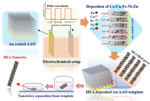
Experimental scheme (Figure ) represents the complete process for preparation, deposition and collection of HEA NWs. Morphological and microstructural details of nanowires, containing all five elements with their stoichiometry, were determined by field emission gun scanning electron microscopy (FEGSEM) and scanning transmission electron microscopy (STEM) assisted with EDS.
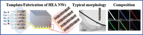
Figure 1. Schematic representation for the synthesis of 1D Co–Cu–Fe–Ni–Zn high-entropy alloy nanowires and illustration of the step-by-step process from the synthesis on AAO template to the separation of nanowires from AAO.
Observations made from FEGSEM (Figure ) revealed that, the synthesized nanowires are very uniform in length and diameter with smooth surface finish. Also, composition of the nanowires along their length is invariant with the presence of all five elements in the HEA composition range (5–35 at. %) throughout the wire (Table ). Furthermore, the uniform composition along the length of the nanowire shows the reliability of the method for complex alloy systems like HEAs. Usually, Fe-based alloys, specifically containing Fe, Co and Ni, follow anomalous behaviour during the deposition [Citation25] which dominates the composition range in the order of Fe > Co > Ni irrespective of the experimental parameters.
Figure 2. FEGSEM micrographs of pulse electrodeposited nanowires separated from Au/AAO template (a) aligned HEA NWs show their uniform length and flexibility (b–c) are the magnified micrographs indicating the uniform distribution in the width of the nanowires prepared by pulse electrodeposition.
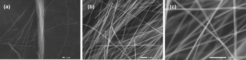
Table 1. Stoichiometry of HEA nanowire throughout the length.
Contrarily, due to the geometrical constraints, such as porous structure of AAO template with pore diameter of 100 ± 20 nm, the composition of alloy directly followed the electrolytic concentration unlike in deposition of thin films. On the other side, duration of the electrodeposition for synthesizing present HEA NWs is a few minutes only unlike the existing studies on electrochemical synthesis of nanowires [Citation26]. In addition, due to the growth in porous structure, several phenomena, which usually occur during the thin film depositions, probably may not occur in the nanowire deposition. For further determination of crystallinity and phase, the nanowires were characterized by TEM.
Representative microstructure of the HEA nanowire is shown in Figure . The low magnification TEM in Figure (a) clearly displays the nanowire length is typical of the order of several microns in size and the diameter is around 100 nm. A bright field TEM image, taken from the individual nanowire of Figure (a), contains several polycrystalline grains, appearing in dark contrast in Figure (b). The SAED pattern also confirmed that nanowire is indeed polycrystalline with random orientation. Furthermore SAED rings (Figure (b)) reveal that individual nanowires are of face-centred cubic (FCC) structure. Polycrystalline features observed in nanowires are due to the application of pulse during the deposition where new nucleation occurs during every pulse ON time. High-resolution TEM of nanowire revealed extremely fine size nanotwin lamellae within a grain, as shown in Figure (c). These twins are oriented along {111} planes, as shown in the inserted fast Fourier transform pattern (FFT) in Figure (c) that lie parallel to nanowire surface and growth direction, and spacing is extremely fine in the range of 1–5 nm.
Figure 3. TEM characterization of nanowires. (a) Low magnification TEM image showing the morphology and average diameter of 100 nm for a wire. (b) Bright field TEM and corresponding SAED pattern display that the nanowire is polycrystalline with FCC structure. (c) High-resolution TEM image taken on the [011] zone axis reveals that the nanowire is composed of nanotwin lamellae with spacing in the range of 1–5 nm on {111} planes.
![Figure 3. TEM characterization of nanowires. (a) Low magnification TEM image showing the morphology and average diameter of 100 nm for a wire. (b) Bright field TEM and corresponding SAED pattern display that the nanowire is polycrystalline with FCC structure. (c) High-resolution TEM image taken on the [011] zone axis reveals that the nanowire is composed of nanotwin lamellae with spacing in the range of 1–5 nm on {111} planes.](/cms/asset/92e8f01a-166f-462f-ad2c-e0d82e0a5ccc/tmrl_a_1896588_f0003_oc.jpg)
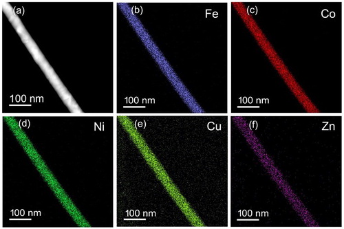
Furthermore, STEM-EDS chemical mapping reveals that the nanowire contains HEA elements of Fe, Co, Ni, Cu and Zn (Figure (a–f)). These five elements are homogenously distributed throughout the nanowire with a defined HEA composition. The chemical composition, obtained from STEM-EDS of several HEA nanowires, is shown in Table S1, which is consistent with SEM-EDS of Table .
Figure 4. STEM-EDS of a nanowire. (a) HAADF-STEM image contrast shows the nanowire is polycrystalline with a grain size of few tens of nanometre in size with random orientation. (b–f) EDS chemical mapping obtained from the region reveals (b) iron (Fe), (c) cobalt (Co), (d) nickel (Ni), (e) copper (Cu) and (f) zinc (Zn), which are uniformly distributed throughout the individual nanowire.
Several reports explained the growth mechanism of single/polycrystalline metal nanowires by 2D/3D nucleation/growth, instantaneous and progressive growth based on the overpotential and kinetics of nucleation [Citation27,Citation28]. However, the growth mechanism of the HEA NWs, especially for an alloy system with five elements is very complex. In the present study, the application of pulse, ON and OFF time plays a significant influence in forming nanowires with uniform composition etc. It is well understood that the growth of the nanowires begins from the Au seed layer which is a back contact for the AAO template. During the pulse condition, potential gradient and mobility of metal ions and their competition led to the growth process [Citation26]. The hydrates/complexes of five elements further reduce its mobility during the reduction process. Therefore, application of pulse in addition to the electrolyte concentration resulted in the formation of nanocrystalline FCC containing multiple elements with uniform composition unlike in conventional DC deposition. But, after OFF time, followed by forward pulse ON time enables the new nucleation having uniform distribution, and filling efficiency of elements throughout the pore homogeneously. On the other side, twin formation in thin films for FCC materials during the pulse electrodeposition is very common [Citation29–31]. In the present deposition, probably due to the five dissimilar ions that fill a very small pore size of 120 nm during pulse leads to a large amount of stress development. Simultaneously during every forward pulse (ON), the stacking arrangement of atoms gets disturbed and may not follow the regular stacking sequence which finally results in faults in the wire which further leads to the formation of twins along the length of the wire [Citation31]. Although the formation-growth mechanism of HEA NWs is yet to be understood, however, the twin formation in HEAs during the deposition can be explained by two reasons: Primarily, due to the evolution of stresses/strains and their relaxation [Citation29,Citation30] during the pulses and secondly, owing to the elements having dissimilar crystal structures such as FCC, BCC (body-centred cubic) and HCP (hexagonally close packed), leading to the generation of dislocations/faults in the stacking sequence of the nanowire, which probably resulting in the formation of nanotwins.
These findings are uncommon for the high-entropy alloy morphologies in the primary attempt, where their large aspect ratio, alloying elements and ultimately a single-phase alloy with highly stable crystal structure. On the other side, the biggest advantage of this study is that these nanowires consist of five transition elements more specifically distinctive entities of iron, cobalt, and nickel present in the alloy makes HEA NWs magnetic. Having magnetic (Fe, Co, Ni), non-magnetic (Cu, Zn) transition elements in HEA NWs and corrosion/oxidation-resistant elements (Ni, Cu, Zn), these NWs are probably an efficient alternative for the existing nanowires with limited functionality in healthcare/device applications. Further modification/engineering of these nanowires in terms of size, aspect ratio, composition, etc., can improve their synergistic effect in revealing their distinctive unexplored functionalities.
Conclusions
We emphasized our study in the direction of the unexplored 1D morphology of high-entropy Co–Cu–Fe–Ni–Zn alloy and reported the primary observations. Nanocrystalline nanowires with FCC structure are reported by an electrochemical approach in a single step using aqueous electrolyte. Application of pulse for the preparation of these nanowires enables the possibility of control over its formation simultaneously with composition and crystallinity which are shown from the microstructural analysis by TEM, STEM etc. Moreover, the formation of twins in HEA NWs of five elements with dissimilar crystal structures may aid in good ductility in this new morphology. The unique combination of Co–Cu–Fe–Ni–Zn HEA nanowires developed by an electrochemical approach facilitates the design of various multifunctional novel nanostructures in the area of HEAs. In addition, being the foremost observation of HEA NWs, this can significantly influence both basic and applied research perspectives of advanced nanomaterials research which is different from its bulk counterparts.
Supplemental Material
Download MS Word (14.4 KB)Acknowledgements
Scanning Electron Microscopy observations were carried out at the Department of Materials Science and Metallurgical Engineering, IIT Hyderabad using the DST-FIST FEGSEM facility. Transmission Electron Microscopy studies were carried out in Frontier Research Center for Materials Science at Shanghai Jiao Tong University, China.
Disclosure statement
No potential conflict of interest was reported by the author(s). C.L.P.P, S.R.D, R.K.S.K.J filed an INDIAN patent (Application No- 202043041990).
Correction Statement
This article has been republished with minor changes. These changes do not impact the academic content of the article.
Additional information
Funding
References
- Ferry DK. Nanowires in nanoelectronics. Science. 2008;319(5863):579–580.
- Garnett E, Mai L, Yang P. Introduction: 1D nanomaterials/nanowires. Chem Rev. 2019;119(15):8955–8957.
- Goktas NI, Wilson P, Ghukasyan A, et al. Nanowires for energy: a review. App Phy Rev. 2018;5(4):041305.
- Martínez-Banderas AI, Aires A, Teran FJ, et al. Functionalized magnetic nanowires for chemical and magneto-mechanical induction of cancer cell death. Sci Rep. 2016;6:35786.
- Geng X, Navarrete E, Liang W, et al. Electrodeposited Fe-Mo-Ni nanowires and Cu-Mo-Fe-Ni alloy nanowire segments. Mater Lett. 2018;211:9–12.
- Maliar T, Cesiulis H, Podlaha EJ. Coupled electrodeposition of Fe–Co–W alloys: thin films and nanowires [original research]. Front Chem. 2019;7(542):1–11.
- Murty BS, Yeh J-W, Ranganathan S, et al. High-entropy alloys. Amsterdam: Elsevier; 2019.
- George EP, Raabe D, Ritchie RO. High-entropy alloys. Nat Rev Mater. 2019;4(8):515–534.
- Miracle DB, Senkov ON. A critical review of high entropy alloys and related concepts. Acta Mater. 2017;122:448–511.
- Li W, Liu P, Liaw PK. Microstructures and properties of high-entropy alloy films and coatings: a review. Mater Res Lett. 2018;6(4):199–229.
- Waag F, Li Y, Ziefuß AR, et al. Kinetically-controlled laser-synthesis of colloidal high-entropy alloy nanoparticles. RSC Adv. 2019;9(32):18547–18558.
- Liu X, Zhang J, Bi S, et al. Chemical complexity in high entropy alloys: a pair-interaction perspective. arXiv Preprint ArXiv. 2019:190710223.
- Oh HS, Kim SJ, Odbadrakh K, et al. Engineering atomic-level complexity in high-entropy and complex concentrated alloys. Nat Commun. 2019;10(1):2090.
- Jin Z, Lyu J, Zhao Y-L, et al. Rugged high-entropy alloy nanowires with in situ formed surface spinel oxide As highly stable electrocatalyst in Zn–Air batteries. ACS Mater Lett. 2020;2(12):1698–1706.
- Gao H, Sun W, Sun Q, et al. Compositional varied core–shell InGaP nanowires grown by metal–organic chemical vapor deposition. Nano Lett. 2019;19(6):3782–3788.
- Shankar KS, Raychaudhuri AK. Fabrication of nanowires of multicomponent oxides: Review of recent advances. Mater Sci Engn: C. 2005;25(5):738–751.
- Wang N, Cai Y, Zhang RQ. Predictions of effective physical properties of complex multiphase materials. Mater Sci Eng: R: Rep. 2008;63(1):1–30.
- Min S-Y, Kim T-S, Kim BJ, et al. Large-scale organic nanowire lithography and electronics. Nat Commun. 2013;4(1):1–9.
- Geissler M, Wolf H, Stutz R, et al. Fabrication of metal nanowires using microcontact printing. Langmuir. 2003;19(15):6301–6311.
- Lupu N. Nanowires: science and technology. London: BoD–Books on Demand; 2010.
- Mohammed H, Moreno JA, Kosel J. Advanced fabrication and characterization of magnetic nanowires. Magn Magn Mater 2017.
- Sarkar J, Khan GG, Basumallick A. Nanowires: properties, applications and synthesis via porous anodic aluminium oxide template. Bull Mater Sci. 2007;30(3):271–290.
- Lupu N. Electrodeposited nanowires and their applications. London: BoD–Books on Demand; 2010.
- Serrà A, Vallés E. Advanced electrochemical synthesis of multicomponent metallic nanorods and nanowires: fundamentals and applications. Appl Mater Today. 2018;12:207–234.
- Dahms H, Croll I. The anomalous codeposition of iron-nickel alloys. J Electrochem Soc. 1965;112(8):771–775.
- Narayanan T, Shaijumon M, Ci L, et al. On the growth mechanism of nickel and cobalt nanowires and comparison of their magnetic properties. Nano Res. 2008;1(6):465–473.
- Hills G, Pour AK, Scharifker B. The formation and properties of single nuclei. Electrochim Acta. 1983;28(7):891–898.
- Scharifker B, Hills G. Theoretical and experimental studies of multiple nucleation. Electrochim Acta. 1983;28(7):879–889.
- Xu D, Kwan WL, Chen K, et al. Nanotwin formation in copper thin films by stress/strain relaxation in pulse electrodeposition. Appl Phys Lett. 2007;91(25):254105.
- Xu D, Sriram V, Ozolins V, et al. In situ measurements of stress evolution for nanotwin formation during pulse electrodeposition of copper. J Appl Phys. 2009;105(2):023521.
- Beyerlein IJ, Zhang X, Misra A. Growth twins and deformation twins in metals. Annu Rev Mater Res. 2014;44:329–363.