

Abstract
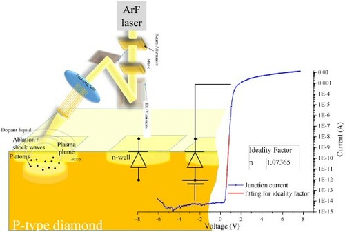
We report the fabrication of p-n+ diamond homojunction through an innovative approach of laser irradiation in liquid-ambient. A shallow phosphorus-doped layer with a high electric conductivity is processed on top of a p-type diamond substrate to form the p-n+ homojunction. The current–voltage measurements at room temperature confirmed high conductivity of the induced n+ layer and showed exceptional rectification properties with an ideality factor of 1.07, excellent low on-resistance of 3.7 × 10⁻² Ωcm2, and current density over 260 Acm−2 at forward-biasing of 10 V. Furthermore, undetectable leakage-current provides a rectification ratio exceeding 1010 at ±6 V, promoting the junction in UV detection applications.
GRAPHICAL ABSTRACT
IMPACT STATEMENT
The process allows further selective and feasible patterned/shallow doping of diamond surfaces beyond the conventional methods, with minimal power consumption and fast production rate, providing more readily electrically contacted devices.
Disclosure statement
No potential conflict of interest was reported by the author(s).
Additional information
Supporting Information is provided for a detailed discussion regarding modeling of ablation temperature, and substrate optical and Raman characterization.
Correction Statement
This article has been corrected with minor changes. These changes do not impact the academic content of the article.