
 ?Mathematical formulae have been encoded as MathML and are displayed in this HTML version using MathJax in order to improve their display. Uncheck the box to turn MathJax off. This feature requires Javascript. Click on a formula to zoom.
ABSTRACT
The effects of varying calcination temperature, K content, and the number of calcination steps in the dielectric performance of KCa2Nb3O10 synthesized via solid-state reaction are investigated. Adding an extra calcination step at 500°C followed by another calcination at 1100°C suppressed the formation of secondary phases while maximizing the relative density (95%) and the average grain area (2.12 μm2). The first calcination at 500°C ensures the formation of intermediate phases (KNbO3 and Ca2Nb2O7), which are prerequisites for single-phase KCa2Nb3O10 synthesis. A significantly high dielectric constant of 352 at 100k Hz is achieved in the two-step calcined sample despite the low sintering temperature of 1250°C. The highest resistivity of the two-step calcined sample (2 × 10⁸ Ω cm) obtained from complex impedance analysis supports its lowest dielectric loss (0.034 at 100k Hz). When the two-step calcined KCa2Nb3O10 powder is exfoliated, much higher dielectric properties of Ca2Nb3O10 nanosheets are expected.
1. Introduction
Two-dimensional (2D) oxide nanosheets have attracted much attention for their potential applications in next-generation electronic devices over the last few years [Citation1,Citation2]. The 2D oxide nanosheets are only a few nm-thick while their length is μm-long. Their unique functionalities can be attributed to the 2D quantum confinement effects, which are not observed in bulk materials [Citation2–8]. Most of the oxide nanosheets are semiconductors with large band gaps (>3 eV) or insulators, and their future applications differ depending on the band gaps [Citation2,Citation9]. While semiconducting oxide nanosheets have been investigated as new materials for channels in field-effect transistors, insulating oxide nanosheets have been developed for new dielectric layers in gate dielectrics or multi-layer ceramic capacitors (MLCCs) [Citation10–12]. By assembling oxide nanosheets with varying electronic properties in a superlattice-like structure, novel functionalities can be designed in nanosheet-based electronics.
Insulating oxide nanosheets are ideal dielectric materials for electronic nanodevices. Currently, BaTiO3 is the most important dielectric material and is heavily used in MLCCs. The thickness of the BaTiO3 films (dielectric layers) in the MLCCs is approximately 0.8 μm [Citation13]. For miniaturization and higher performance of the MLCCs, the thickness of dielectric layers is required to be further reduced. However, because the dielectric constant (εr) of BaTiO3 nanoparticles is more than 10 times lower than that of BaTiO3 submicron particles, a drastic εr collapse is observed in the BaTiO3 thin films of <100 nm thickness [Citation14]. For example, the εr of (Ba1-xSrx)TiO3 thin film of thickness <20 nm is less than 35 (εr of the bulk BaTiO3: ~3000) [Citation1]. In contrast, dielectric oxide nanosheets do not experience any εr collapse with decreasing nanosheet thickness. Ca2Nb3O10 is one of the most extensively studied oxide nanosheets due to its excellent dielectric performance [Citation15]. The εr of Ca2Nb3O10 oxide nanosheet is as high as 200, and it does not change even when its thickness is decreased from ~20 down to ~5 nm [Citation1]. Therefore, the dielectric oxide nanosheets are promising candidates for dielectric layers in the miniaturized MLCCs.
The Ca2Nb3O10 oxide nanosheets are obtained by exfoliation of KCa2Nb3O10 bulk layered perovskite [Citation16]. The interlayer K+ ions are first exchanged into H+ ions to form HCa2Nb3O10 via acid-exchange reactions [Citation17]. The protonated layered perovskite is then delaminated through intercalation of bulky tetrabutylammonium ions to produce Ca2Nb3O10 oxide nanosheet suspension [Citation18]. In other words, the dielectric properties of Ca2Nb3O10 oxide nanosheets are closely correlated to those of bulk KCa2Nb3O10 layered perovskite. However, the number of literatures which investigated the dielectric properties of KCa2Nb3O10 layered perovskite is limited. Li et al. focused more on the impact of adding perovskite layer on dielectric properties of KCa2Nan−3NbnO3n+1 (n = 3–6), where n = 3 corresponded to KCa2Nb3O10 [Citation19]. They reported the εr of KCa2Nb3O10, but materials parameters related to εr were not discussed in detail. Kweon et al. thoroughly discussed various factors that affected the dielectric properties of KCa2Nb3O10 layered perovskite. They concluded that the εr of KCa2Nb3O10 calcined at 900°C followed by sintering at 1375°C was the highest (~46 at 100k Hz) with the average grain size greater than 30 μm. Here, we demonstrate that two-step calcination (500 & 1100°C) effectively achieves high dielectric properties in KCa2Nb3O10 layered perovskite. When the two-step calcination is applied to KCa2Nb3O10 with subsequent sintering in a reducing atmosphere at 1250°C (followed by annealing in air at 1000°C), a significantly high εr of ~352 (at 100k Hz) is obtained even when the average grain area is smaller than 3 μm2. We expect the dielectric properties of Ca2Nb3O10 oxide nanosheets exfoliated from the two-step calcined KCa2Nb3O10 layered perovskites to be higher than that exfoliated from the conventionally calcined KCa2Nb3O10.
2. Experimental procedures
2.1. KCa2Nb3O10 preparation
KCa2Nb3O10 powder was synthesized by solid-state reactions from high-purity K2CO3 (>99.995%, Sigma-Aldrich, St. Louis, U.S.A.), CaCO3 (>99.95%, Sigma-Aldrich, St. Louis, U.S.A.), and Nb2O5 (>99.99%, Sigma-Aldrich, St. Louis, U.S.A.) powders. K2CO3, CaCO3, and Nb2O5 were weighed (1) stoichiometrically, (2) with 10%, and (3) 20% excess of K2CO3. Three different mixed powders were ball-milled with zirconia balls (3 and 5 mm in diameter) and ethanol for 18 hours. Once the ball-milled slurries were dried using a vacuum oven (80°C for 12 hours), the dried powders were ground with a mortar and pestle. Some of the stoichiometric powders were single-step calcined at 500, 700, 900, and 1100°C for 10 hours. The rest were two-step calcined first at 500°C (10 or 20 hours), followed by another calcination at 1100°C (10 hours). 10% and 20% K excess powders were calcined at 1100°C for 10 hours. The powders prepared via three different routes were first compacted (10 mm diameter and 1.5 mm thickness) under isostatic pressure of 250 MPa for 3 minutes using a cold isostatic press (CIP; Sansho Industry, Osaka, Japan), and subsequently sintered at 1250°C for 2 hours in a reducing atmosphere (5% H2/N2), followed by annealing at 1000°C for 1 h in the air.
2.2. Materials characterization
The crystal structure and phases of KCa2Nb3O10 powders and bulk samples were characterized by X-ray diffraction (XRD; Smartlab, Rigaku, Tokyo, Japan) analysis. The relative densities of KCa2Nb3O10 bulk samples were estimated using the Archimedes’ principle. Frequency-dependent dielectric responses and complex impedances (1k – 1 M Hz) of the KCa2Nb3O10 bulk samples were analyzed at room temperature using a precision LCR meter (E4980A, Keysight, California, USA). Eutectic InGa alloy is used as electrode material. It is rubbed on both surfaces of the samples before the dielectric property measurements. The microstructures of polished KCa2Nb3O10 bulk samples were characterized using field-emission scanning electron microscopy (FE-SEM; SU5000, Hitachi, Osaka, Japan). Image quality (IQ), phase maps, and average grain size areas of the polished KCa2Nb3O10 bulk samples were analyzed with electron backscatter diffraction (EBSD; Velocity Super, Edax, Berwyn, U.S.A.).
3. Results and discussion
) presents the X-ray diffraction (XRD) patterns of KCa2Nb3O10 (KCNO) powder with a varying K content, calcined at different calcination conditions. First, stoichiometric KCNO powder was calcined from 500 to 1100°C for 10 hours (“K1.0 – calcination temperature °C/10 h” in )). Secondly, KCNO powder with 10% and 20% excess K was calcined at 1100°C for 10 hours to compensate for possible K evaporation during the calcination at high temperatures (“K1.1 or K1.2–1100°C/10 h”). Lastly, the stoichiometric KCNO powder was calcined in a two-step heating process. The two-step heating process included the first calcination at 500°C for 10 or 20 hours, followed by another calcination at 1100°C for 10 hours (“K1.0–500°C/10 or 20 h + 1100°C/10 h”). The two-step heating process was adopted to minimize the amount of second phases formed after the calcination. The reason for choosing 500°C as the first calcination temperature is provided below.
Figure 1. X-ray Diffraction (XRD) patterns of KCa2Nb3O10 (a) powder of varying K content after calcining at different calcination conditions, and (b) bulk samples after sintering at 1250°C for 2 hours.
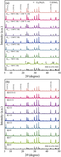
When the single-step calcination was applied to stoichiometric KCNO powder, only those calcined at 900 and 1100°C crystallized to a monoclinic lattice with a P21/m space group [Citation20]. The XRD pattern for “K1.0–700°C/10 h” powder showed peaks for Ca2Nb2O7 and KNbO3 (noted with circle and rectangle symbols, respectively, in )), in addition to the peaks corresponding to KCNO. However, the XRD peaks for “K1.0–500°C/10 h” powder mostly consisted of Ca2Nb2O7 and KNbO3 peaks. Ca2Nb2O7 and KNbO3 are the intermediate phases that are formed before KCNO when the starting materials for KCNO are calcined together [Citation21]:
The fact that XRD peaks for Ca2Nb2O7 and KNbO3 coexist for the KCNO powder calcined at 500°C (“K1.0–500°C/10 h”) suggests that the two intermediate phases are synthesized near 500°C. Synthesis of a single-phase KCNO is only guaranteed when syntheses of intermediate phases are successful. For this reason, the two-step calcination at 500 and 1100°C was designed in the first place. Besides, significant K evaporation was not observed at calcination temperatures ≤1100°C because the CaNb2O6 phase, which was related to the evaporation of K, was not detected via the XRD analysis.
Nonetheless, 10% and 20% of excess K2CO3 was mixed with other starting materials in Eqn. (1) to investigate the effect of K excess on the synthesis of KCNO. Because the 1100°C calcination temperature was not high enough to evaporate a significant amount of K, increasing the amount of excess K2CO3 increased the amount of Ca2Nb2O7 and KNbO3 phases, as shown in the XRD peaks of “K1.1–1100°C/10 h” and “K1.2–1100°C/10 h”. The off-balance between the intermediate phases due to increased K2CO3 input might be responsible for the remaining intermediate phases even after the calcination.
Adding an extra calcination step at 500°C before calcining at 1100°C allowed extra time for the syntheses of Ca2Nb2O7 and KNbO3. The dwelling time at 500°C was varied from 10 to 20 hours to see if the longer dwelling time affected the synthesis of KCNO. Both “K1.0–500°C/10 h + 1100°C/10 h” and “K1.0–500°C/20 + 1100°C/10 h” formed phase pure KCNO just as “K1.0–1100°C/10 h” did.
) shows the XRD peaks for KCNO bulk samples sintered at 1250°C under a reducing atmosphere (1% H2/N2) for 2 hours, followed by annealing at 1000°C in the air for 1 h. The sintering/annealing conditions used in the MLCC manufacturing were also adopted here. Because all the samples were sintered and annealed under the same conditions, each sample was identified by its calcination conditions. Depending on the content of K used to synthesize the KCNO powder, K0 (K1.0 – stoichiometric), K1 (K1.1–10% excess), and K2 (K1.2–20% excess) were used in their abbreviated sample names. Calcination conditions were summarized by their calcination temperature divided by 100 for simplicity, without calcination time, as the majority of the samples were calcined for 10 hours at the calcination temperature (if 1100°C/10 h → 11). Two-step calcination conditions were expressed as “first calcination temperature/second calcination temperature”. For example, the KCNO sample with “K1.0–500°C/10 h + 1100°C/10 h” calcination condition was expressed as “K0-5/11”. When the first calcination at 500°C lasted for 20 hours, we named the sample “K0-5/5/11” as “5” meant calcination at 500°C for 10 hours, and “5/5” could be understood as 500°C calcination for 20 hours. The abbreviated names for the KCNO bulk samples are also provided in ). No secondary phases were observed in all the KCNO bulk samples, regardless of the K contents and calcination conditions. The Ca2Nb2O7 and KNbO3 intermediate phases previously detected in some of the KCNO powder ()) were no longer present in the sintered KCNO bulk samples ()). According to Kweon et al., the intensities of XRD peaks corresponding to (0 0 2), (0 0 4), (0 0 6), (0 0 8), and (0 0 14) of the KCNO bulk samples sintered at temperatures higher than 1350°C were significantly increased compared to those observed in KCNO powder [Citation21]. Rod-like grains abnormally grown perpendicular to <0 0 2> directions were responsible for the increased peak intensities. However, such significant increases in the peak intensities are not observed in ) when compared to ) because the sintering temperature was only 1250°C. Corresponding microstructures of the KCNO bulk samples will be discussed below.
shows the dielectric properties of the KCNO bulk samples sintered at 1250°C. The calcination temperature, K content, and the number of calcination steps of the KCNO samples before sintering were all different. The εr and dielectric losses (tan δ) of the bulk samples were measured for frequencies ranging from 1k to 1 M Hz with 0 direct current (DC) bias and 1 Vrms at room temperature ()). The εr and tan δ of all samples decreased with increasing frequency, but the rates of decrease in εr and tan δ were much suppressed at frequencies higher than 100k Hz. The relationship between εr at 100k Hz and the relative density (ρr) of the samples are also provided in ). ) shows the frequency-dependent εr and tan δ of KCNO samples with different calcination temperatures (single-step calcination). As the calcination temperature increased, the corresponding εr increased at all frequencies. The εr of the “K0-11” sample was the highest among the samples calcined at temperatures between 500 and 1100°C. The εr of “K0-11” was approximately 323 at 1k Hz, decreasing to 230 at 100k Hz. The dielectric loss of “K0-11” also decreased from 2.09 to 0.097 as the frequency increased from 1k to 100k Hz, respectively. According to Kweon et al., the εr of the KCNO sample sintered at 1375°C was 46 with a dielectric loss of 0.009 at 100k Hz. The 100k Hz εr of “K0-11” is approximately 5 times higher than that reported by Kweon et al. [Citation21]. The tan δ of the KCNO samples increases with a decreasing frequency (≤100k Hz). This behavior can be attributed to the low-frequency dispersion or dc conductivity. To find out which mechanism is responsible for the observed behavior, frequency-dependent electrical conductivity measurement is required. If a finite gradient is exhibited in the frequency-dependent electrical conductivity at low frequency, we can conclude that the low-frequency dispersion is active in the KCNO samples [Citation22,Citation23]. ) shows how the 100k Hz εr and ρr change with an increasing calcination temperature. The ρr of the samples also increased with the calcination temperature even when the sintering temperature was fixed. The highest εr of “K0-11” can be attributed primarily to its ρr (70%), higher than those of other single-step calcined samples in ) (48–65%). Given that the ρr of the KCNO sample (sintered at 1375°C) from Kweon et al. was almost 97%, the much low ρr of “K0-11” (70%) could be responsible for its high tan δ [Citation24,Citation25].
Figure 2. Room temperature dielectric constants (εr) and losses (tan δ in log-scale) of KCNO bulk samples with different (a) calcination temperature, (c) K content, and (e) number of calcination steps measured from 1k to 1 M Hz with 0 direct current (DC) bias and 1 Vrms. The εr (at 1k and 100k Hz) and relative densities (ρr) of the samples corresponding to (a, c, and e) are provided in (b, d, and f), respectively.
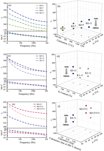
) shows the frequency-dependent εr and tan δ of the KCNO samples with varying K content. Except for the K content, calcination and sintering conditions were kept constant. The “K0-11” in ) is identical to that presented in ). Varying K content did not alter εr much at 1k Hz, but the rate of εr decrease with increasing frequency was the highest in “K1-11”. Hence, the εr of “K1-11” at 100k Hz (194) was the lowest among the samples with different K content. That of “K2-11” (223) was higher than that of “K1-11”, but slightly lower than that of “K0-11” (230). ) shows that increasing K content improves the ρr of the samples. For example, the ρr of “K2-11” (78%) was approximately 11% higher than that of “K0-11”. If the ρr is the only factor that affects εr, the εr of “K2-11” should have been higher than that of “K0-11”. However, the fact that the εr of “K0-11” is higher than “K2-11” suggests that the εr of intermediate phases (Ca2Nb2O7 and KNbO3) is confirmed to be present in “K2-11”, are lower than that of KCNO. When the εr of “K2-11” is compared to that of “K1-11”, we see that the εr of “K2-11”, which has a higher amount of intermediate phases, is higher than that of “K1-11”. The εr of the two intermediate phases must be different, and when the two phases are both present in a sample, the overall εr should depend on the molar ratio between the two phases. In other words, “K2-11” may include one of the intermediate phases with higher εr more than “K1-11”.
) shows the εr and tan δ of two-step calcined KCNO samples. The single-step calcined “K0-11” is also provided for comparison. Adding one more calcination step at 500°C much improved εr and significantly suppressed tan δ (<100k Hz) simultaneously, compared to those of “K0-11”. Enhanced dielectric properties of the two-step calcined samples can be attributed to their ρr (88–95%) being much higher than that of “K0-11” (70%) ()). Between the two-step calcined samples, the ρr of “K0-5/11” (95%) is higher than that of “K0-5/5/11” (88%). Possible particle agglomeration due to the prolonged calcination at 500°C (20 hours) in “K0-5/5/11” may have impeded the densification during sintering. As a result, the εr of “K0-5/11” (352) is higher than that of “K0-5/5/11” (330) at 100k Hz. The 100k Hz εr of “K0-5/11” is approximately 43% higher than that of “K0-11”, and almost 7.7 times higher than that reported by Kweon et al. (46) [Citation21]. The dielectric loss of “K0-5/11” at 100k Hz is as low as 0.034.
Dielectric properties of three different groups of KCNO samples were compared. The first group changed the calcination temperature ()), the second group varied the content of K ()), and the last group added another calcination step ()). From each group of samples, the one with the highest εr was selected to further investigate factors that determined its observed dielectric properties (“K0-11” from ), “K2-11” from ), and “K0-5/11” from )). Although the εr of “K0-11” was also highest in ), “K2-11”, whose εr was the second highest, was selected instead to study the effect of varying K content in various factors correlated to dielectric properties. The dielectric property measurements provided in are made on the polished samples. However, depending on the surface condition of the samples their dielectric properties may be different [Citation26,Citation27]. The effect of surface condition on dielectric properties is tested on “K0-11” sample. The “K0-11” sample with unpolished surface exhibits slightly higher εr than the polished sample. The εr difference between the unpolished and polished “K0-11” increases with increasing frequency. At the 1 M Hz, the εr of the unpolished “K0-11” is higher than that of the polished “K0-11” by approximately 10%.
shows image quality (IQ) and phase maps of “K0-11”, “K2-11”, and “K0-5/11” obtained by Electron Backscatter Diffraction (EBSD) analysis. Fractured cross-sections of the samples were polished for EBSD mapping. The three samples have plate-like grains according to the IQ maps in ). The average length and width of the plate-like grains were observed to increase with the excess K (“K2-11”) or extra calcination step (“K0-5/11”). While the average area of the grains was the largest in “K0-5/11”, that of the pores (dark regions in )) were the smallest in “K0-5/11” as well. Abnormally grown rod-like grains (>30 μm in length) previously observed by Kweon et al. were not observed here due to low sintering temperature.
Figure 3. Electron Backscatter Diffraction (EBSD) image quality (IQ) maps and phase maps (KCNO, KNbO3, Ca2Nb2O7, and CaNb2O6 phases in red, blue, yellow, and green) of (a, b) “K0-11”, (c, d) “K2-11”, and (e, f) “K0-5/11”. The average grain sizes and areas of the samples are provided in the insets of (a, c, and e) and (b, d, and f), respectively.
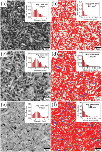
Red, blue, yellow, green, and white regions in ) represent KCNO, KNbO3, Ca2Nb2O7, CaNb2O6 phases, and pores, respectively. While KNbO3 and Ca2Nb2O7 are the intermediate phases formed before KCNO is synthesized (Eqn. (1)), the CaNb2O6 phase is the secondary phase formed due to K evaporation during calcination or sintering. Although none of the phases other than KCNO were detected in the XRD analysis of the three samples (), a small amount of KNbO3, Ca2Nb2O7, and CaNb2O6 phases were detected in the color-coded phase maps of the EBSD analysis. Area fractions of KCNO, KNbO3, Ca2Nb2O7, CaNb2O6 phases, and pores in different samples are provided in .
Table 1. Area fractions of KCNO, KNbO3, Ca2Nb2O7, CaNb2O6 phases, and pores in “K0-11”, “K2-11”, and “K0-5/11” samples.
The area fraction of the KCNO phase in “K0-5/11” was the highest among the three samples. Moreover, the total area fraction of other phases (KNbO3, CaNb2O6, and Ca2Nb2O7) was also the highest in “K0-5/11”. As a result, the area fraction of pores in “K0-5/11” was the lowest, which was reasonable given that the ρr of “K0-5/11” was the highest among the three samples ()). The area fractions of CaNb2O6 and Ca2Nb2O7 were the lowest in “K0-5/11”, but that of KNbO3 was higher than that of “K0-11” and “K2-11”. Nonetheless, the area fraction ratio of KNCO to other phases is the highest in “K0-5/11”, confirming that the two-step calcination (“K0-5/11”) is effective in suppressing the formation of phases other than KCNO.
In addition to the phase analysis, the average grain areas of “K0-11”, K2-11’, and “K0-5/11” were also estimated by the EBSD analysis (insets of )). When calculating the average grain areas of the samples, phases other than KCNO were not included. Instead of average grain size in diameter, the average grain area is used to better represent the size of plate-like grains [Citation28]. The average grain area of “K0-11” was approximately 1.31 μm2. The average grain size area of “K2-11” (2.07 μm2) was larger than that of “K0-11” by 58%. The average grain area of “K0-5/11” (2.21 μm2) was even greater than that of “K0-11” by more than 69%. The highest ρr of “K0-5/11” can be attributed to the largest grains of the three samples, facilitating the densification.
Figure 4. εr (100k Hz) of “K0-11”, “K2-11”, and “K0-5/11” as functions of average grain size area, area fraction of KCNO phase, and ρr.
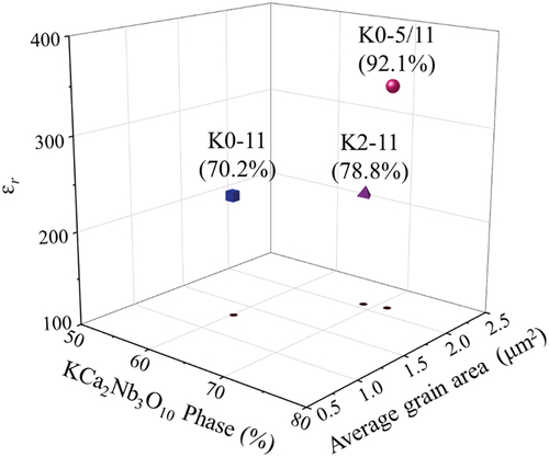
summarizes how the εr of “K0-11”, “K2-11”, and “K0-5/11” are related to average grain size area, KCNO phase area fraction (both via EBSD), and ρr. “K0-5/11” with the highest average grain size area, KCNO area fraction, and ρr among the three samples has the highest εr. The additional calcination step in “K0-5/11” has facilitated the grain growth and suppressed the formation of phases other than KCNO, while achieving a high ρr. Because large grain size, single-phase, and high sample density are known to improve εr, the εr of 352 at 100k Hz is achieved in “K0-5/11”. It is even higher than that reported by Li et al. (300) by 17% [Citation19]. However, there must be another factor affecting the εr other than grain size, KCNO phase, and ρr to explain the εr of “K2-11” slightly lower than that of “K0-11” despite its higher average grain size area, KCNO area fraction, and ρr.
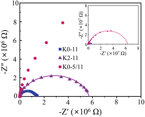
shows the complex impedances of “K0-11”, “K2-11”, and “K0-5/11” measured at room temperature. The (-Z´, -Z˝) data points in (in symbols) are the measurements, and the lines are fitting curves that describe the data. The x–intercepts of the fitted semi-circles represent the resistances of the samples. While the resistances of “K0-11” (1.5 × 10⁶ Ω) and “K2-11” (5.8 × 10⁶ Ω) are in the same order, that of “K0-5/11” amounts to 6.2 × 10⁷ Ω. When the disk-type sample dimensions are taken into account (~9 mm in diameter with ~1 mm thickness), the resistivities of “K0-11”, “K2-11”, and “K0-5/11” are approximately 5 × 10⁶, 2 × 10⁷, and 2 × 10⁸ Ω cm, respectively. Relatively low resistivities of the KCNO samples when compared to other dielectric materials (BaTiO3 > 1011 Ω cm) explain the higher εr and tan δ of the samples at low frequencies (<100k Hz) than those measured at higher frequencies. The conducting K+ ions between the layers of KCNO samples are responsible for the low-frequency dispersion [Citation29]. According to Kweon et al., the resistivity of the KNCO sample sintered at 1350°C is 2.5 × 10⁷ Ω cm, which is similar to that of “K2-11” (2 × 10⁷ Ω cm). The resistivities of the samples are well reflected in their tan δ near 1k Hz (low frequency). The tan δ of the “K0-11” (2.09) with the lowest resistivity is the highest, and that of the “K0-5/11” with the highest resistivity is the lowest (0.21). In contrast, high resistivity is not beneficial for εr at low frequencies when the low-frequency dispersion is active. However, the εr of “K0-5/11” is also the highest because its grain size, KCNO phase area fraction, and ρr outweigh its high resistivity.
Figure 5. Cole-Cole plots of “K0-11”, “K2-11”, and “K0-5/11” measured with 1 Vrms at room temperature. The fitted semi-circle for “K0-5/11” is presented in the inset.
4. Conclusions
In summary, the effects of varying calcination temperature, K content, and the number of calcination steps in the dielectric properties of KCa2Nb3O10 (KCNO) bulk samples were investigated. Once the sintering at 1250°C followed by annealing at 1000°C was applied to all calcined KCNO powder, no phase other than KCNO was detected in the X-ray Diffraction (XRD) analysis. Increasing calcination temperature improved the relative density (ρr) of the samples after sintering and the corresponding dielectric constant (εr) (230 at 100k Hz when calcined at 1100°C). Adding excess K to compensate for possible K evaporation during calcination and sintering also increased the ρr of the sample. However, the εr of the sample without excess K was slightly higher than that with 20% K excess (223). When the two-step calcination (500°C followed by 1100°C) was applied to the powder without excess K, its εr was the highest (352) among other single-step calcined samples with or without K excess. The first calcination step at 500°C allowed enough time to form intermediate phases (KNbO3, Ca2Nb2O7) required to synthesize the KCNO successfully. The two-step calcination was found particularly effective in increasing the average grain size area (better indicator in rod-like grains) and relative density while suppressing the formation of secondary phases. The low dielectric loss of the two-step calcined sample was attributed to its high resistivity characterized via complex impedance measurement. Much improved dielectric properties of Ca2Nb3O10 nanosheet are expected when the two-step calcined KCNO powder is used for subsequent ion-exchange and exfoliation to obtain nanosheets.
Acknowledgments
This work was financially supported by the National Research Foundation of Korea (NRF), funded by the Ministry of Education (NRF-2019R1C1C1005632, NRF-2015R1A6A1A03031833). This work was also supported by the Technology Innovation Program RS-2022-00144027 funded by the Ministry of Trade, Industry & Energy (MOTIE, Korea)
Disclosure statement
No potential conflict of interest was reported by the author(s).
Additional information
Funding
References
- Osada M, Sasaki T. Two-dimensional dielectric nanosheets: novel nanoelectronics from nanocrystal building blocks. Adv Mater. 2012;24(2):210–228.
- Osada M, Sasaki T. Exfoliated oxide nanosheets: new solution to nanoelectronics. J Mater Chem. 2009;19(17):2503–2511.
- Bhimanapati GR, Lin Z, Meunier V, et al. Recent advances in two-dimensional materials beyond graphene. ACS Nano. 2015;9(12):11509–11539.
- Sasaki T, Watanabe M, Hashizume H, et al. Macromolecule-like aspects for a colloidal suspension of an exfoliated titanate. pairwise association of nanosheets and dynamic reassembling process initiated from it. J Am Chem Soc. 1996;118(35):8329–8335.
- Schaak RE, Mallouk TE. Prying apart ruddlesden−popper phases: exfoliation into sheets and nanotubes for assembly of perovskite thin films. Chem Mater. 2000;12(11):3427–3434.
- Liu Z-H, Ooi K, Kanoh H, et al. Swelling and delamination behaviors of birnessite-type manganese oxide by intercalation of tetraalkylammonium ions. Langmuir. 2000;16(9):4154–4164.
- Fukuda K, Nakai I, Ebina Y, et al. Colloidal unilamellar layers of tantalum oxide with open channels. Inorg Chem. 2007;46(12):4787–4789.
- Xu T-G, Zhang C, Shao X, et al. Monomolecular-layer Ba5Ta4O15 nanosheets: synthesis and investigation of photocatalytic properties. Adv Funct Mater. 2006;16(12):1599–1607.
- Sasaki T, Watanabe M. Semiconductor nanosheet crystallites of Quasi-TiO 2 and their optical properties. J Phys Chem B. 1997;101(49):10159–10161.
- Kingon AI, Maria J-P, Streiffer SK. Alternative dielectrics to silicon dioxide for memory and logic devices. Nature. 2000;406(6799):1032–1038.
- Niinistö J, Kukli K, Heikkilä M, et al. Atomic layer deposition of High- k oxides of the group 4 metals for memory applications. Adv Eng Mater. 2009;11(4):223–234.
- Robertson J. High dielectric constant gate oxides for metal oxide Si transistors. Rep Prog Phys. 2005;69(2):327–396.
- Kishi H, Mizuno Y, Chazono H. Base-metal electrode-multilayer ceramic capacitors: past, present and future perspectives. Jpn J Appl Phys. 2003;42:1–15.
- Petzelt J. Dielectric grain-size effect in high-permittivity ceramics. Ferroelectrics. 2010;400(1):117–134.
- Akatsuka K, Haga M-A, Ebina Y, et al. Construction of highly ordered lamellar nanostructures through Langmuir−Blodgett deposition of molecularly thin titania nanosheets tens of micrometers wide and their excellent dielectric properties. ACS Nano. 2009;3(5):1097–1106.
- Schaak RE, Mallouk TE. Perovskites by design: a toolbox of solid-state reactions. Chem Mater. 2002;14(4):1455–1471.
- Treacy MMJ, Rice SB, Jacobson AJ, et al. Electron microscopy study of delamination in dispersions of the perovskite-related layered phases K[Ca2Nan-3NbnO3n-1]: evidence for single-layer formation. Chem Mater. 1990;2(3):279–286.
- Han Y-S, Park I, Choy J-H. Exfoliation of layered perovskite, KCa2Nb3O10, into colloidal nanosheets by a novel chemical process. J Mater Chem. 2001;11(4):1277–1282.
- Li B-W, Osada M, Ebina Y, et al. Impact of perovskite layer stacking on dielectric responses in KCa2Nan−3NbnO3n+1 (n = 3–6) Dion–Jacobson homologous series. Appl Phys Lett. 2010;96(18):182903.
- Tokumitsu T, Toda K, Aoyagi T, et al. 層状ペロブスカイト KCa2Nb3O10 の粉末中性子回折による構造決定. J Ceram Soc Jpn. 2006;114(1333):795–797.
- Kweon S-H, Im M, Han G, et al. Sintering behavior and dielectric properties of KCa2Nb3O10 ceramics. J Eur Ceram Soc. 2013;33(5):907–911.
- Wu J, Nan C-W, Lin Y, et al. Giant dielectric permittivity observed in Li and Ti doped NiO. Phys Rev Lett. 2002;89(21):217601.
- Jonscher AK. Dielectric relaxation in solids. J Phys D: Appl Phys. 1999;32(14):R57–R70.
- Mackrodt WC, Davey RJ, Black SN, et al. The morphology of α-Al2O3 and α-Fe2O3: the importance of surface relaxation. J Cryst Growth. 1987;80(2):441–446.
- Penn SJ, Alford NM, Templeton A, et al. Effect of porosity and grain size on the microwave dielectric properties of sintered alumina. J Am Ceram Soc. 1997;80(7):1885–1888.
- Krohns S, Lunkenheimer P, Ebbinghaus SG, et al. Colossal dielectric constants in single-crystalline and ceramic CaCu3Ti4O12 investigated by broadband dielectric spectroscopy. J Appl Phys. 2008;103(8):084107.
- Tuichai W, Thongyong N, Danwittayakul S, et al. Very low dielectric loss and giant dielectric response with excellent temperature stability of Ga3+ and Ta5+ co-doped rutile-TiO2 ceramics. Mat Des. 2017;123:15–23.
- Benzing JT, Liu Y, Zhang X, et al. Experimental and numerical study of mechanical properties of multi-phase medium-Mn TWIP-TRIP steel: influences of strain rate and phase constituents. Acta Mater. 2019;177:250–265.
- Thangadurai V, Weppner W. Electrical properties of A´Ca2Nb3O10 (A´ = K, Rb, Cs) layered perovskite ceramics. Ionics. 2001;7(1–2):22–31.