
 ?Mathematical formulae have been encoded as MathML and are displayed in this HTML version using MathJax in order to improve their display. Uncheck the box to turn MathJax off. This feature requires Javascript. Click on a formula to zoom.
Abstract
The design and analysis of step impedance resonator (SIR) based, compact and band-notch UWB antenna, to minimize the potential interference between wide-band (UWB) and narrow-band (WLAN), has been presented in this paper. The notched band covers the 5.15 GHz to 5.85 GHz WLAN range. The frequency band has been obtained by embedding a SIR near the radiating patch of the antenna. The empirical relationship between the SIR design and band-notch characteristics has also been included in the paper. The UWB patch antenna structure is feed by micro-strip line. The parametric-analysis by varying the parameters the SIR as well as the substrate has been performed, to observe the optimal performance the proposed antenna. The design and functional simulation of the proposed antenna structure is performed by using HFSS-v14. A close agreement between simulated and experimental results for the proposed design has been observed and presented in this paper. The design and results provide ample justification for compatibility and application of the structure in UWB communication over the entire frequency range.
Public Interest Statement
Wireless connectivity has enabled a new mobile lifestyle filled with conveniences for mobile computing users. Consumers will soon demand the same conveniences throughout their digital home, connecting their PCs, personal digital recorders, digital cameras, high-definition TVs, personal digital assistants, and cell phones, to connect to each other in a wireless personal area network (WPAN) in the home. But today’s wireless LAN and WPAN technologies cannot meet the needs of tomorrow’s connectivity of such a host of emerging consumer electronic devices that require high bandwidth. Ultra-wideband (UWB) technology offers a solution for the bandwidth, high data rates across multiple devices, cost, power consumption, and physical size requirements of next-generation consumer electronic devices for digital home and the office. In this context, the UWB antenna design plays a unique role because it behaves like a band pass filter and reshapes the spectra of the pulses and avoid undesired distortions.
1. Introduction
The Ultra wideband (UWB) is a wireless communication technology, which provide a short-range communication from 4 meters to10 meters, with a low output power and high data rate (up to 1 Gbps) in 3.1–10.6 GHz the frequency range (Federal Communications Commission, Citation2002). Some other narrowband applications such as, IEEE802.11a (5–6 GHz) and WiMAX (3.3–3.6 GHz) also exists along with the UWB range (Agrawall, Kumar, & Ray, Citation1998) (Chu & Yang, Citation2008). Therefore, the design of an UWB antenna with band-notch characterstics is a prime requirement to diminish the potential interference between UWB and co-existing narrowband services.
The micro-strip antennas are popular in a wide variety of applications due to their low profile, simple design, conformability to planar and non-planar surfaces, low cost and ease in manufacture with modern printed circuit technology. The radiating patch can be square, rectangular, bow-tie, circular or any other shape. However, the bow-tie configuration is generally preferred in UWB applications because of its ability for bandwidth enhancement and miniaturization (Bahadori & Samii, Citation2007; Schantz, Wolenec, & Myszka, Citation2003; Yao, Huang, & Feng, Citation2007). Recent researches have shown significant interest in the design and analysis of UWB antenna systems in the wireless communication (Da Xu et al., Citation2015; Kadam, Gudino, Ramesha, & Nagaraju, Citation2016; Min, Zhang, Zhong, & Chen, Citation2016).
The main challenge in UWB antenna design is to achieve impedance matching and bandwidth control in simultaneity along with high radiation efficiency and low EMI effects (Daniels, Citation1996; Kerkhoff & Ling, Citation2007; Shaman & Hong, Citation2007). The planar antenna feature is also desirable given that there are several additional constraints and challenges for the design of a UWB antenna system (Choi, Kim, Hwang, & Choi, Citation2014; Chung, Hong, & Choi, Citation2007; Ma & Wu, Citation2007; Ojaroudi, Ojaroudi, & Ghadimi, Citation2013; Ojaroudi, Yazdanifard, Ojaroudi, & Sadeghzadeh, Citation2011; Yang, Jin, Vittoria, Harris, & Sun, Citation2008; Zhang et al., Citation2008). The design and validation of SIR based compact bow-tie antenna with band rejection characteristics is the prime objective of this paper. In this design, the ground plane structure has been taken uneven. The concluding part of the Paper presents a parametric analysis by including various design parameters such as SIR and a ground plane.
2. Antenna design
The parametric analysis of the proposed compact band-rejection antenna structure is based on transmission line modal analysis (Chen, Chia, & Ammann, Citation2003). The detailed geometry and parameters of the proposed antenna structure are depicted in Figure and Table respectively. The simulation results for the proposed antenna structure are obtained with uneven ground patch followed by the parametric analysis of various design parameters of the system.
Figure 1. Top view of proposed band-reject antenna using SIR.
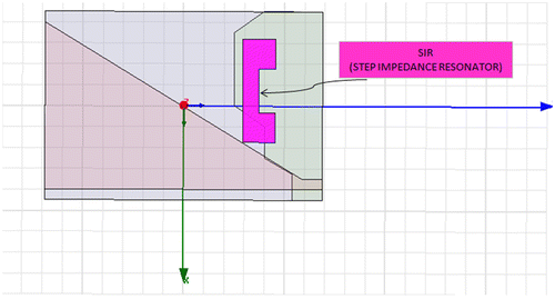
Table 1. Design parameters of proposed antenna
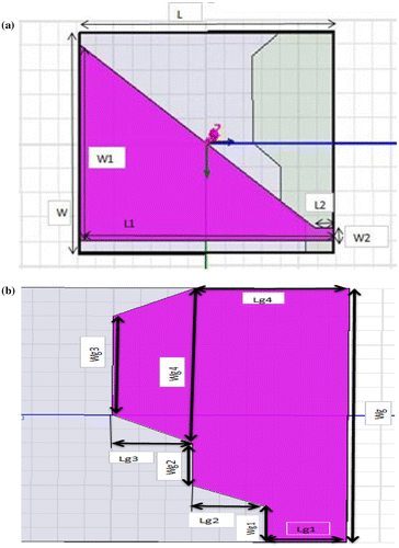
The proposed design has the dimension of 18 × 27.5 mm2 fabricated on the Taconic RF60 substrate with a thickness of 0.64 mm and relative dielectric constant of 6.15, which is having loss tangent (tan δ) 0.0023. The width W2 of the micro-strip feed line is fixed at 1 mm.
Figure depicts the detailed structure of the compact band-rejection antenna, on the upper surface of the substrate, a half bow-tie shape radiating patch shown in Figure (a) and the uneven ground plane shown in Figure (b) respectively.
Figure 2. (a) Geometry of radiating patch and (b) Geometry of ground plane structure.
By embedding a resonator, it is observed that rejection of WLAN band can be accomplished for the proposed structure, thus it is beneficial to minimizing the EMI problem between UWB and WLAN. The resonator referred in this model is a step impedance resonator. From the electrical viewpoint, it is a non uniform transmission line, i.e. a transmission line with the cross section varying in steps and each step is having a different electrical length and impedances. As per the wave cancellation theory, when two signals with identical properties and a phase shift of 180º interact with each other at a particular frequency, the resultant signal becomes zero at that particular frequency.
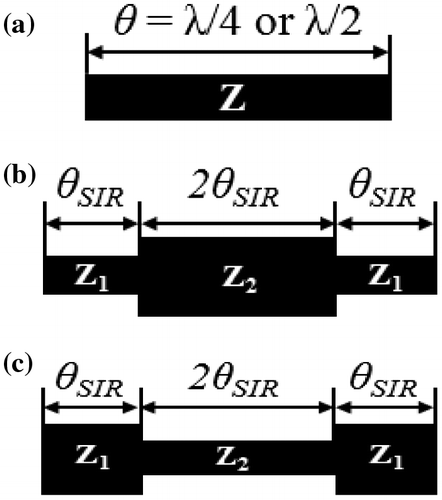
The structure of SIR referred to in this paper is a series combination of different impedances as depicted in Figure (b) and (c). The SIRs generate second harmonics depending upon the difference of SIR impedances, which is responsible for creating the band rejection. The second harmonics and the length of transmission line are determined by the following equations (Lee, Kim, Kim, & Yu, Citation2006):
Figure 3. Types of impedance resonator: (a) Unitary impedance resonator. (b) & (c) Types of step impedance
(1)
(1)
(2)
(2)
(3)
(3)
Equations (1)–(3) show that the frequency of the second harmonics, which is two times of the base frequency in the unitary impedance resonator. Therefore, it can be predicted that the second harmonics would be generated at frequencies given by the following conditions:
f s2 < 2 f 0, when K < 1
f s2 > 2 f 0, when K > 1 (4)
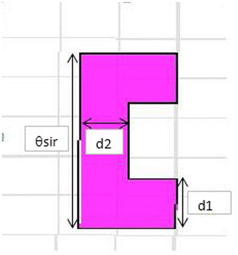
The conditions given in Equation (4) shows the second harmonic frequency can be adjusted in accordance with the variables in the equation. The initial length of the SIR (θSIR) is predetermined by the center frequency of the stop band. The most important design parameters to be decided are the gap, d1 and d2 of SIR as depicted in the geometry of Figure .
Figure 4. Geometry of SIR.
3. Simulation results
Figure shows the simulated return losses (S parameter) of the antenna having multi-band characteristic in the UWB spectrum.
Figure 5. Simulated return loss of designed antenna structure.
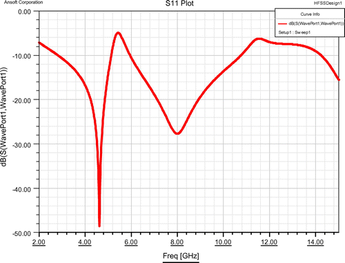
It is observed from Figure that the UWB antenna covers 2.8 –10.8 GHz range with a return loss less than −10 dB except the rejection band 5.15–5.9 GHz. The result indicates that the proposed antenna structure is having return loss less than −10 dB, which is fairly low over the entire UWB range.
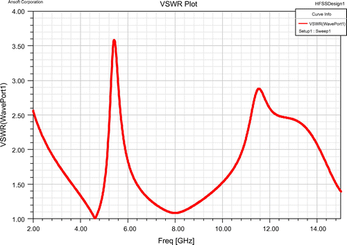
The VSWR of the proposed antenna structure with optimized parameters is shown below in Figure . It is observed from the Figure that the simulated VSWR characteristic of the proposed antenna possesses one exact band notch or frequency rejection band with 5.15–5.9 GHz for WLAN.
Figure 6 Simulated VSWR characteristic of the proposed antenna structure.
4. Parametric analysis
4.1. Effect of variation of the position of SIR
The plot depicted below in Figure shows the comparison of characteristics corresponding to different RL curves pertaining to variation in the position of the resonator (SIR) in X-axis.
Figure 7. Effect of variation of the position of SIR w.r.t. radiating patch in x-axis on the S11(return loss) curve.
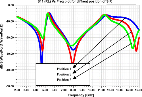
The variation in the position of SIR in X-axis causes a change in the bandwidth of the stop-bands shown in Table . There exists a relation between the two i.e. the position of SIR and the bandwidth of the stop band. Nearer positioning of SIR to radiated patch results in larger bandwidth of the stop-band, while further positioning results in smaller bandwidth of stop-band.
Table 2. Simulated Results corresponding to the variation of position of the resonator (SIR)
4.2. Effect of Variation of Initial Length of SIR
The plot depicted below in Figure shows a comparison of the characteristics to different RL curves corresponding to variation in the initial length of the resonator.
Figure 8. S11 Vs frequency curve for different initial lengths of SIR.
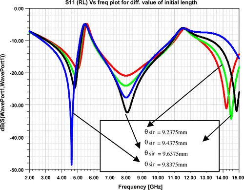
Table shows that the variation in the initial length of SIR causes a change in the center frequency of the stop-band. There exists a relation between the two i.e. the initial length of SIR and the Centre Frequency of the rejection band. A greater length of the SIR results in smaller central frequency of the stop-band and vice versa.
Table 3. Simulation result of variation of initial length θsir of SIR
4.3. Effect of Variation of d1, d2 of SIR on the covered bandwidth
It is observed form Figure that a RL curve corresponding to different widths d1 and d2 of the step impedance resonator and proves the relation between the two d1, d2 and bandwidth. It is observed that an increase in d1 and d2 decreases the bandwidth of the proposed antenna and vice versa, which is indicated in Table .
Figure 9. S11 Vs frequency curve for different width d1, d2 of SIR.
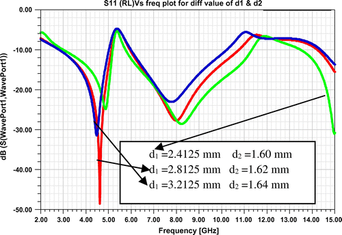
Table 4. the simulation result of variation of width d1, d2 of SIR
4.4. Effect of Variation of Substrate material
The curve depicted below in Figure shows the effect of the variation of substrate material of the proposed UWB Antenna structure without any tunning in antenna dimensions.
Figure 10. Effect of Variation of Substrate material of the proposed UWB antenna structure.
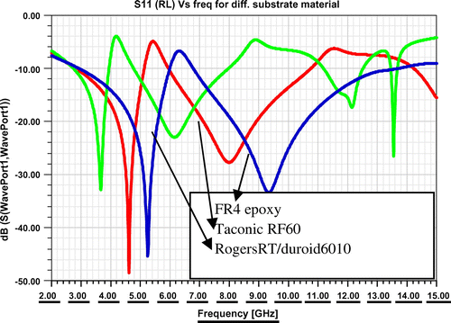
FR4-epoxy has a lowest value of εr in the substrate materials included in Table , which is implying larger bandwidth than other two dielectric materials at the cost of Q-factor. At the same time the dielectric Taconic RF60-A has a moderate value of covered bandwidth, which is sufficient for UWB application with low loss tangent δ implying low energy losses in the material. Similarly Rogers RT/duroid6010 have high Q-factor, but less bandwidth, which cannot fulfill the requirement of UWB application. These attributes justify Taconic RF60-A dielectric as appropriate for fabrication of the proposed antenna structure.
Table 5. Effect of variation of different substrate material.
4.5. Effect of variation of substrate thickness
The graph depicted below in Figure shows the effect of the variation of substrate thickness of the proposed UWB antenna structure on its covered bandwidth resonant frequency performance.
Figure 11. Effect of Variation of Substrate thickness of the proposed UWB antenna structure.
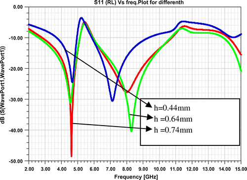
The thickness of the substrate is increased progressively from h = 0.44 to 0.74 mm in three steps. It is observed that:
| (a) | The increase in substrate thickness h then increases the fringing fields at the edges, which in turn increases the effective length L of the patch, thereby reducing the resonant frequency of the system. This apart, the increase in h reduces W/h ratio, thus reducing effective relative permittivity εeff of the dielectric causing increase in resonant frequency of the system. One important observation is made as, the performance of the antennais increase as εr decrease. Therefore, the net effect of the variation in substrate thickness is the overall decrease the resonance frequency due to the dominance of the effect of varying Leff. Hence, when the thickness (h) is increased from 0.44 to 0.74 mm, the resonant frequency decreases from 4.69 to 4.54 GHz. | ||||
| (b) | As h is increased from 0.44 to 0.74 mm, the impedance bandwidth increases from 5,620 to 8,150 MHz. Therefore, by increasing the substrate thickness, the bandwidth can be enhanced. But, the substrate thickness cannot be increased beyond an extent as that would make surface waves dominant. This necessitates judicious selection of substrate thickness for realizing higher bandwidth. | ||||
This justifies the selection of substrate thickness, h = 0.64 mm in the instant case as it results in a large bandwidth.
4.6. Effect of Variation of width Wg of ground
The curve depicted below in Figure shows the effect of the variation of width of ground plane relating to the proposed UWB Antenna structure.
Figure 12. Effect of Variation of ground plane width of the proposed antenna structure.
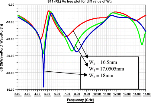
It is observed that the antenna bandwidth increases as the ground width Wg is increased and vice versa shown in Table and Figure above. At a specific value of ground plane width, there is an impedance matching and a minimum return loss is achieved (see Figure ).
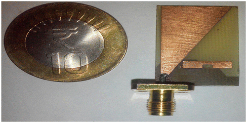
Figure 13. Fabricated photograph of proposed antenna structure.
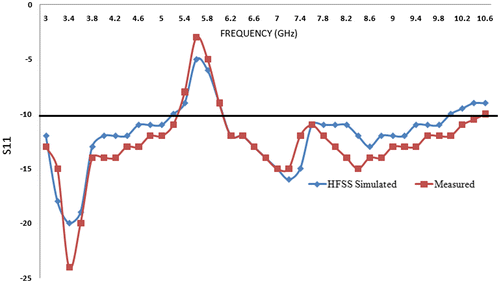
The measured and simulated S11 of the proposed antenna with single band notch characteristics shown Figure . The measurement of S11 was carried out with a network analyzer Agilent N5230 (10 MHz to 20 GHz). A relatively good agreement between measurement and simulation has been observed. It is found that the input impedance of the fabricated antenna is well matched as the bandwidth covers the entire UWB band (3.1–10.6 GHz).
Figure 14. Comparitive graph for simulated and measured S11 of the proposed UWB Antenna structure.
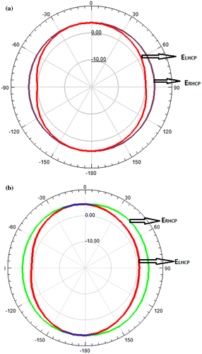
The axial ratios are often quoted for antennas in which the desired polarization is circular. The ideal value of the axial ratio for circularly polarized fields is 0 dB. In addition, the axial ratio tends to degrade away from the mainbeam of an antenna, so the axial ratio may be indicated in a data sheet for an antenna as follows:
Axial Ratio < 3 dB for ± 30 degrees from main beam.
This indicates that the deviation from circular polarization is less than 3 dB over the specified angular range (see Figure ).
Figure 15. Comparitive graph for simulated ERHCP and ELHCP of the proposed UWB antenna structure (a) at 4 GHz and (b) at 8 GHz.
The axial ratio can be calculated from:(5)
(5)
And the cross polarization is:(6)
(6)
(7)
(7)
where; XPD is cross polarization.
5. Conclusion
This work, as evidenced from the characteristic curves and Tables – included in the paper has been successfully designed and realized the proposed microstrip antenna structure with a half bow-tie patch and miniaturization, which makes it suitable for UWB applications. The proposed antenna has impedance bandwidth covering the entire UWB range (2.8–10.8 GHz), along with rejection-band in the WLAN (5.15–5.85 GHz). A prototype antenna is fabricated by using low-cost Taconic RF60 substrate. Overall, the performance of the proposed antenna meets the desired requirements in terms of return loss (<−10 dB) and VSWR (<2).
Table 6. Effect of substrate thickness on bandwidth
Table 7. Simulation result with the variation of ground plane width Wg of the proposed structure
Additional information
Funding
Notes on contributors
Tejbir Singh
Tejbir Singh has completed his Bachelors (B.Sc.) and Masters (M.Sc.) CCS University, Meerut in 2004 and 2006 respectively. He has also completed his Master of Technology (M.Tech) in Communication Engineering from VIT University, Vellore in 2010. He is pursuing his Ph.D. in the Electronics Department of Banasthali University, Jaipur, Rajasthan, India.
Heena Choudhary
Heena Choudhary is currently an assistant professor in the Department of ECE, SVS University; Meerut, India.
D.V. Avasthi
D.V. Avasthi is working as a professor in SVS University, Meerut, UP, India.
Vishant Gahlaut
Vishant Gahlaut is working as a assistant professor in Banasthali University, Banasthali, Rajasthan, India. His research area is Microwave Electronics.
References
- Agrawall, N. P., Kumar, G., & Ray, K. P. (1998). Wide-band planar monopole antennas. IEEE Transactions on Antennas and Propagation, 46, 294–295.10.1109/8.660976
- Bahadori, K. & Samii, Y. R. (2007). A Miniaturized Elliptic-Card UWB Antenna With WLAN Band Rejection for Wireless Communications. IEEE Transactions on Antennas and Propagation, 55, 3326–3332.
- Chen, Z. N., Chia, M. W. Y., & Ammann, M. J. (2003). Optimization and comparison of broadband. Proceedings of the Institution of Electrical Engineers, 150, 429–435.
- Choi, H. S., Kim, T. W., Hwang, H. Y., & Choi, K. (2014). An UWB antenna design with adjustable second rejection band using a SIR. IEEE Transactions on Magnetics, 50, 913–916.10.1109/TMAG.2013.2283774
- Chung, K., Hong, S., & Choi, J. (2007). Ultrawide-band printed monopole antenna with band-notch filter. IET Microwaves, Antennas & Propagation, 1, 518–522.10.1049/iet-map:20050356
- Chu, Q. X., & Yang, Y. Y. (2008). A Compact Ultrawideband Antenna With 3.4/5.5 GHz Dual Band-Notched Characteristics. IEEE Transactions on Antennas and Propagation, 56, 3637–3644.
- Daniels, D. J. (1996). Surface-penetrating radar. Proceedings of the Institution of Electrical Engineers, 6, 72–93.
- Da Xu, K., Zhang, Y. H., Spiegel, R. J., Fan, Y., Joines, W. T., & Liu, Q. H. (2015). Design of a stub-loaded ring-resonator slot for antenna applications. IEEE Transactions on Antennas and Propagation, 63, 517–524.
- Federal Communications Commission. (2002). Federal Communications Commission revision of part 15 of the commission’s rules regarding ultra-wideband transmission system from 3.1 to10.6 GHz. Washington, DC: Author.
- Kadam, B. V., Gudino, L. J., Ramesha, C. K., & Nagaraju, S. (2016). A band-notched ultra-wideband compact planar monopole antenna with u-shaped parasitic element. Procedia Computer Science, 93, 101–107.10.1016/j.procs.2016.07.188
- Kerkhoff, A. J., & Ling, H. (2007). Design of a band-notched planar monopole antenna using genetic algorithm optimization. IEEE Transactions on Antennas and Propagation, 55, 604–610.10.1109/TAP.2007.891563
- Lee, W. S., Kim, D. Z., Kim, K. J., & Yu, J. W. (2006). Wideband planar monopole antennas with dual band-notched characteristics. IEEE Transactions on Microwave Theory and Techniques, 54, 2800–2806.
- Ma, T. G., & Wu, S. J. (2007). Ultrawideband band-notched folded strip monopole antenna. IEEE Transactions on Antennas and Propagation, 55, 2473–2479.10.1109/TAP.2007.904137
- Min, X.-L., Zhang, H., Zhong, T., & Chen, Q. (2016). Design of an UWB antenna with adjustable rejection bandwidth using novel Dual-T square resonator. Progress In Electromagnetics Research Letters, 64, 87–92.10.2528/PIERL16101501
- Ojaroudi, M., Ojaroudi, N., & Ghadimi, N. (2013). Dual band-notched small monopole antenna with novel coupled inverted U-ring strip and novel fork-shaped slit for UWB applications. IEEE Antennas and Wireless Propagation Letters, 12, 182–185.10.1109/LAWP.2013.2245296
- Ojaroudi, M., Yazdanifard, S., Ojaroudi, N., & Sadeghzadeh, R. A. (2011). Band-notched small square-ring antenna with a pair of T-shaped strips protruded inside the square ring for UWB applications. IEEE Antennas and Wireless Propagation Letters, 10, 227–230.10.1109/LAWP.2011.2131630
- Schantz, H. G., Wolenec, G., & Myszka, E. M. (2003). Frequency notched UWB antennas. In Proceedings of the Conference on IEEE Ultra Wideband Sys. Technologies (pp. 214–218), Reston, VA.10.1109/UWBST.2003.1267835
- Shaman, H., & Hong, J. S. (2007). Ultra-wideband (UWB) bandpass filter with embedded band notch structures. IEEE Microwave and Wireless Components Letters, 17, 193–195.10.1109/LMWC.2006.890467
- Yang, G. M., Jin, R., Vittoria, C., Harris, V. G., & Sun, N. X. (2008). Small ultra-wideband (UWB) bandpass filter with notched band. IEEE Microwave and Wireless Components Letters, 18, 176–178.10.1109/LMWC.2008.916781
- Yao, Y., Huang, B., & Feng, Z. H., (2007). A novel ultra-wideband microstrip-line fed wide-slot antenna having frequency band-notch function. In 2007 ICMMT’07 Proceedings of the International Conference on Microwave and Millimeter Wave Technologies (pp. 1–4), Guilin.
- Zhang, Y., Hong, W., Yu, C., Kuai, Z.-Q., Don, Y.-D, & Zhou, J.-Y. (2008). Planar ultra wide band antennas with multiple notched bands based on etched slots on the patch and/or split ring resonators on the feed line. IEEE Transactions on Antennas and Propagation, 56, 3063–3068.10.1109/TAP.2008.928815