
 ?Mathematical formulae have been encoded as MathML and are displayed in this HTML version using MathJax in order to improve their display. Uncheck the box to turn MathJax off. This feature requires Javascript. Click on a formula to zoom.
Abstract
High efficiency ultrathin CdTe film is an excellent candidate for reliable, efficient, stable and low cost solar cells. In this paper, a high efficiency CdS/CdTe solar cell has been studied by using ADEPT 1D simulation tool. The proposed device has been simulated with a reduced CdTe absorber layer thickness and a ZnTe layer as back surface field (BSF) which substantiates sensible energy conversion efficiency. The investigation into the simulation results showed that the conversion efficiency with BSF layer and 1 μm thick CdTe absorber is 8.24% more as compared to the conventional CdTe cells (without BSF layer). Reduction of minority carrier recombination loss due to the insertion of BSF layer at the back contact in ultra-thin CdS/CdTe cells has also been investigated. The results depict that CdTe cell with BSF layer is responsible for increasing the quantum efficiency. However, the proposed structure of ZnO/CdS/CdTe/ZnTe demonstrates the highest efficiency of 24.66% (Voc = 946.51 mV, Jsc = 34.40 mA/cm2 and FF = 75.72%) under global AM1.5G illumination spectra.
Public Interest Statement
Photovoltaic solar cells based on CdTe (Cadmium Telluride) absorber are considered to be the most effective type of thin film solar cells. It has high energy conversion efficiency, long term stability and industrial scalability. This research article presents a numerical model of CdTe based solar cell, which was simulated under standard illumination conditions. Different material parameters were varied to obtain the maximum result from the cell. It was proved that the simulated cell is valid while comparing with the previously experimental reference cell. Evidently, a linear increase was found in the open-circuit voltage and short-circuit current density. This study introduces a back surface field layer which reduces minority carrier recombination loss at the back contact and enhances the overall cell performance. Therefore, this cell structure could be used to fabricate cost effective, thin film and highly efficient CdTe cell.
1. Introduction
Polycrystalline Cadmium Telluride (CdTe) is perceived as a very promising absorber layer material for highly efficient thin-film solar cells. It is an II–VI semiconductor used in the photoelectric devices for its high absorption coefficient > 5 × 105 cm−1 (Lee & Gray, Citation1993; Wu, Citation2004). However, the direct optical bandgap of CdTe is 1.48 eV which matches intimately to sunlight spectrum (Zhao et al., Citation2016). Hence, the thickness required for an absorption layer of CdTe cells makes the cost of material relatively low. Apparently, one of the primary objectives of modern solar cell research is the cost reduction of semiconductor material by making the cells thinner. Thinning will decrease the production cost by saving materials, reducing the recombination loss and production time (Aramoto et al., Citation1997; Ferekides et al., Citation2000). Furthermore, under AM1.5G illuminations for terrestrial usage the CdTe thin film solar cells have shown high efficiency and long-term durable performance (Aramoto et al., Citation1997). CdTe solar cell with total area efficiency of 16.5% has been obtained using chemical bath deposited (CBD) CdS buffer layer (Wu, Citation2004). The close spaced sublimation (CSS) process is also used to fabricate CdS/CdTe solar cells instead of using CBD process. High deposition rates and efficient material utilization are the attractive features of CSS technology for large area applications (Ferekides et al., Citation2000). A high short-circuit current density has been found in CdTe solar cell while integrating ZnxCd1−xS as a window layer. In fact, 19.5% efficiency was achieved with CdTe thickness of 1 μm (Hossain et al., Citation2011). Below this thickness there is a serious degradation of the efficiency because of sharp losses in short-circuit current density (Jsc), open-circuit voltage (Voc), and in some cases, fill factor (FF) (Hossain et al., Citation2011). The thickness optimization of CdTe absorption layer to around 1 μm shows potential increase in the efficiency and the insertion of higher bandgap materials (i.e. ZnTe) at the back contacts can reduce carrier recombination loss. ZnTe can produce a back surface field (BSF) to inhibit the minority carrier loss at the back contact (Amin, Yamada, & Konagai, Citation2002). Up to now, the CdTe based solar cell has reached to the highest experimental efficiency of 22.1% (Green et al., Citation2017) although the theoretical limit exceeds 24%. However, various strategies for improving efficiency are currently being considered with low-cost fabrication technologies.
The proposed CdS/CdTe solar cell has been modeled using drift-diffusion simulator ADEPT 2.1 (Gray et al., Citation2015). By using this simulator, a number of researches have been done by several researchers. Chavali, Johlin, Gray, Buonassisi, and Alam (Citation2016) have consistently dealt with the effect of the cell-to-module efficiency gap discovered in a-Si/c-Si heterojunction solar cell by scrutinizing the process-to-module modeling framework. Haque and Galib (Citation2013) have shown that the choice of absorber layer material with optimized doping density and thickness measurement of different layers are crucial steps to obtain 20% cell efficiency for III-V semiconductor based ultrathin-film solar cells. Furthermore, by using this simulator, the impacts of absorber band gap and doping level of each layers of Cu(In1−xGax)Se2 (CIGS) solar cell have been evaluated through the consequences of drift velocity and recombination rate (Asaduzzaman, Hasan, & Bahar, Citation2016). Asaduzzaman, Hosen, Ali, and Bahar (Citation2017) has also conducted a CIGS solar cell simulation with different buffer layers and compared the simulated results with the experimental works in the literature.
In this paper, firstly we extracted the physical parameters of the constituent materials from an experimental work as a reference cell (Mahabaduge et al., Citation2015), simulated with these parameters using ADEPT and compared the simulated results with the reference cell for validation purpose. Afterwards, we propose a ZnTe BSF in corporation with a polycrystalline CdTe thin film solar cell. The effect of absorber layer thickness and the ZnTe BSF on the cell performance have also been studied in order to optimize the cell efficiency. The quantum efficiencies have also been analyzed for different CdTe cell structures and finally the cell efficiency has been optimized.
2. Device structure and numerical simulation
In this study, numerical simulation of an n-ZnO/n-CdS/p-CdTe/p-ZnTe solar cell is a crucial step in the analysis of its structure and properties. A one-dimensional simulation software, ADEPT 2.1 has been employed to simulate the electrical characteristics of hetero-structured semiconductor devices. It resolves Poisson’s equation matched with the hole and electron continuity equations in one spatial dimension. Energy band diagram, dark I–V characteristics, light I–V characteristics, electric field distribution and the spectral response of solar cells etc. can be figured out by this software. Different layer material parameters like thickness, band gap, mobility, electron affinity etc. are employed as inputs in ADEPT simulator. Hetero-structured solar cell devices constructed from semiconductor materials for which these parameters can also be simulated.
The primary purpose of this research is to attain an ultra-thin film high efficiency CdTe solar cell. At the beginning we compared all the simulation results of the experimental CdTe reference cell (Mahabaduge et al., Citation2015) with our designed and simulated CdTe cell. Figure shows the schematic structure of the reference cell and the proposed n-ZnO/n-CdS/p-CdTe/p-ZnTe thin film solar cell used for guiding the simulation.
Figure 1. Schematic structure of (a) CdTe reference cell (Mahabaduge et al., Citation2015) and (b) Proposed CdTe solar cell with BSF layer.
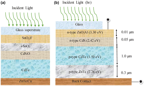
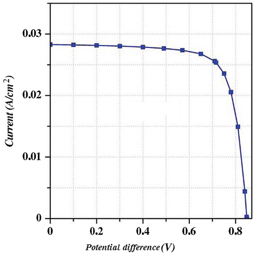
The reference cell was composed with a SnO2: F as TCO, i-SnO2, CdS and CdTe. The glass superstrate and Cu doped ZnTe were used as front and back contacts respectively. The experimental results of this reference cell presented a short-circuit current density of 25.52 mA/cm2, an open-circuit voltage of 0.831 V, a fill factor of 77.43% and an efficiency of 16.42% under AM1.5G conditions. For validation purpose of the simulation, we have simulated the same device structure as reference cell and Table equates the performance parameters of the reference cell with ADEPT 2.1 simulation results. The simulated J–V characteristics curve has been dictated in Figure .
Table 1. Output parameters of the reference cell (Mahabaduge et al., Citation2015) and proposed CdTe solar cell
Figure 2. J–V characteristic curve of the reference cell simulation for validation purpose using ADEPT 2.1.
The physical parameters used in the CdS/CdTe/ZnTe solar cell simulation are shown in Tables and (Amin et al., Citation2002, Citation2011; Aramoto et al., Citation1997; Asaduzzaman, Bahar, & Bhuiyan, Citation2017; Asaduzzaman, Bahar, Masum, & Hasan, Citation2017; Gessert et al., Citation1997; Hossain et al., Citation2011; Lee & Gray, Citation1993; Mahabaduge et al., Citation2015; Mirkamali & Muminov, Citation2016).
Table 2. Default values of the device parameters used in simulation
Table 3. Contact layer parametric values used for simulation
In this analysis, the thickness of the CdTe absorber layer has been fixated as 1 μm. Absorber thickness reduction can be done by controlling the temperature profile during the CSS process. Basically, high substrate temperature is applied during the CSS CdTe deposition and it is one of the principal reason that CdS/CdTe solar cells achieved high efficiencies. The CSS technology (Ferekides et al., Citation2000) can produce large grain films compared to processes such as electro deposition, sputtering, physical vapor deposition etc. The loss at the back contact due to carrier recombination can no longer be neglected in such thin CdTe solar cells. Therefore, a wider band gap material ZnTe (band gap of 2.26 eV) is inserted prior to the back contact to inhibit the recombination of the generated carriers by pressurizing them back to the CdS/CdTe junction (Amin et al., Citation2002; Mirkamali & Muminov, Citation2016). This may reduce the contact resistance and increase the cell efficiency.
The short circuit current density, Jsc depends on the spectrum of the incident light and the optical properties (recombination, reflection, absorption). In CdTe based solar cell, Jsc can be calculated by the following formula (Mohamed, Citation2013):
(1)
(1)
Where q is the charge of an electron, T(λ) is the optical transmission, фi is the spectral power density, and Δλi is the interval between the two adjacent values of wavelength.
The open circuit voltage, Voc, arises when the net current through the solar cell is zero and can be expressed as (Paudel, Wieland, & Compaan, Citation2012):
(2)
(2)
The fill factor, FF, finds out the maximum power of a solar cell and can be expressed as (Singh & Ravindra, Citation2012):
(3)
(3)
Here, is specified as “normalized Voc”.
The incident illumination is AM1.5G spectra during the calculation of the J–V characteristics in this numerical analysis as it is a standard terrestrial illumination (Aramoto et al., Citation1997). And the energy conversion efficiency of a solar cell, η, is given by (Paudel et al., Citation2012):
(4)
(4)
The input power, Pin, from the sun is regarded as 1000 W/m2.
3. Results and discussions
In CdTe solar cells, cadmium sulfide (CdS) has been used as a thin window layer and the Al-doped ZnO is employed to develop transparent contact. But the back contacts express a non-ohmic behavior in the J–V characteristics of CdTe cell. This situation is known as Schottky barrier which reduces the performance of the solar cell. Hence, ZnTe has been introduced as an intermediate semiconductor to increase the conductivity with a tunneling barrier.
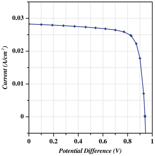
ADEPT 1D simulation was employed to determine the appropriate thickness and bandgap of CdTe and ZnTe layer using the number of variable parameters. The simulation was conducted with the default values summarized in Tables and and a light J–V characteristics graph was obtained as shown in Figure . The values of open circuit voltage (Voc = 940.79 mV) and short circuit current (Jsc = 28.26 mA/cm2) were obtained from the curve. Then the fill factor (FF) and the efficiency (η) were calculated as 76.92% and 20.45% respectively.
Figure 3. J–V characteristics curve for default values of CdTe solar cell.
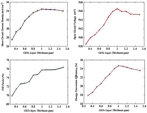
In this study, a CdTe solar cell with absorber layer thickness of 1 μm and band gap of 1.50 eV has been simulated. The absorber layer thickness is one of the important parameter because of its effect on material usage and cost. It can affect the CdTe cell’s performance. In a thin absorber layer, the back contact is located near the depletion region and the incoming photons with lower energy are absorbed deep into the absorber layer. Thus some part of photo-generated carriers will be recombined at the back contact and accordingly will decrease the cell performance (Khoshsirat, Md Yunus, Hamidon, Shafie, & Amin, Citation2015). However, the CdTe absorber layer thickness has been changed from 0.3 to 1.5 μm throughout the simulation. The cell’s output parameters vary because of the increase in absorber layer thickness as shown in Figure . The results show that the performance becomes better while increasing the thickness of the absorber. It can also be resolved that the absorber layer thickness cannot be increased overly and it still requires an optimization. Optimum performance has been found out at 1 μm thickness of CdTe absorber layer. An open-circuit voltage (Voc) of 946.50 mV has been obtained, while the short-circuit current density (Jsc) is 34.40 mA/cm2. Consequently, the fill factor is calculated as 75.72% which in turn results in conversion efficiency of 24.66%. It is observed that for the thickness above 1 μm, Voc, Jsc, FF and η increase marginally and sometimes decrease. As a matter of fact, by further increasing absorber layer thickness, a number of incoming photons will be absorbed into the absorber layer and the resulting carriers cannot reach to the space charge region. Thus the possibility of bulk recombination can raise due to increasing absorber layer thickness (Khoshsirat et al., Citation2015; Mohamed, Citation2013).
Figure 4. Effect of CdTe thickness on solar cell performance parameters.
In order to fabricate an efficient and long-term stable CdS/CdTe solar cell, major challenges associated in the formation of a low resistance, stable, non-rectifying contact to p-type CdTe thin film (Sabaghi, Majdabadi, Marjani, & Khosroabadi, Citation2015). The main difference of thin film cells compared to the thicker ones is that the back contact interface located nearer to the CdS/CdTe junction. This distinctly establishes the effect in thin CdTe cells, carrier recombination occurs near at the back contact. Thus the choice of the back contact material consequently has a high impact on the cell performance.
In this investigation, a wide band-gap material ZnTe (Eg = 2.26 eV) has been introduced at the back contact making a CdTe/ZnTe hetero-junction interface to suppress the possible recombination loss at the back contact of ultra-thin CdTe solar cell. The simulation has been conducted for variation in ZnTe layer thicknesses within the range from 0.01 to 0.5 μm. The simulation result shows that at 0.3 μm thickness, the energy conversion efficiency is optimum. Figure shows the effect of ZnTe thickness on CdTe cell performance. The ZnTe layer acts as a BSF which limits the flow of minority carriers from the base to the rear surface of the cell. During the simulation, doping concentration of ZnTe was kept fixed to 1 × 1018 cm−3 because of high built-in electrical field and higher absorption level. Table shows the comparison between output parameters of different simulated CdTe cells with the reference cell.
Figure 5. Effect of ZnTe BSF layer thickness on the cell performance.
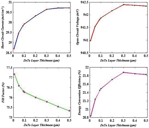
Table 4. Comparison between performance of proposed CdTe solar cell and reference cell
It is observed from Table that the conventional CdTe cell without any BSF layer shows conversion efficiency of 16.42%. When ZnTe is inserted as a BSF, the conversion efficiency increases to 24.66% and the current density Jsc improved a bit due to reduced minority carrier recombination loss at the back contact.
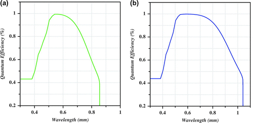
The external quantum efficiency (EQE) has derived as a function of wavelength. The spectral response for different CdTe cells from ADEPT simulation is shown in Figure . The operating wavelength ranges from 300 to 1100 nm. At longer wavelengths, the QE is zero due to the photon energy below the bandgap. The graph shows that the spectral response of CdTe/ZnTe cell is often greater than the CdS/CdTe cell. It is also clear that ZnTe layer can increase the carriers by reflecting them back towards the CdS/CdTe interface. While measuring the quantum efficiency spectrum the Jsc has increased from the value of 24.47 mA/cm2 (without ZnTe) to 34.40 mA/cm2 (with ZnTe) and hence improving the efficiency of the CdTe solar cell.
Figure 6. EQE curve of the cells (a) without ZnTe and (b) with ZnTe BSF layer.
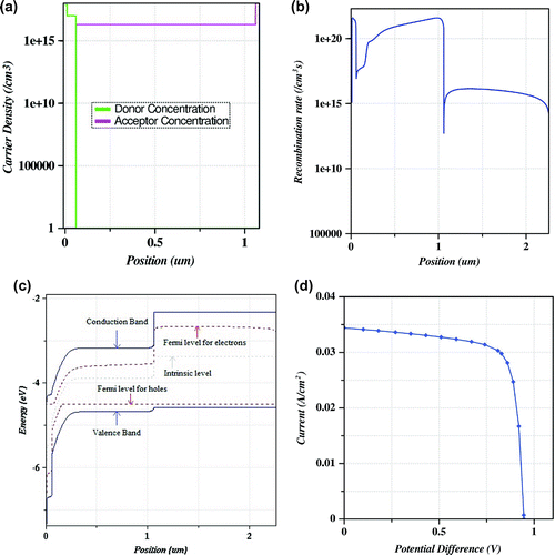
From the analysis, the thickness of the absorber layer is optimized as 1 μm. The insertion of 0.3 μm thick ZnTe layer contribute to produce potentially higher efficiency. Figure (a) depicts the doping concentrations of different layers of CdTe solar cell whereas Figure (b) represents the recombination rate corresponding to the thickness of the cell. The energy band diagram shows that the ZnTe BSF layer is enormously beneficial for minority carrier reflection as shown in Figure (c). Finally, Figure (d) represents the J–V characteristic curve from which the optimum efficiency (η = 24.66%) for CdTe cell has been estimated.
Figure 7. (a) Doping concentration (b) Recombination profile (c) Energy band diagram and (d) J–V characteristics curve of optimized CdTe solar cell.
4. Conclusions
This paper introduces an extensive performance analysis due to the effect of absorber layer thickness with a ZnTe BSF layer in a CdS/CdTe solar cell. Numerical modeling of CdTe hetero-structure thin film solar cell was performed using ADEPT 2.1 one-dimensional online simulator. Simulation with default parameters demonstrated that the conversion efficiency was increased about 4.03% in comparison with the reference cell. The CdTe cell performance was troubled by the back surface recombination in the case of thinner CdTe absorbers. But the computations related to CdS/CdTe/ZnTe structure indicates that insertion of ZnTe could completely overcome the back surface recombination loss and importantly increases the cell efficiency. ZnTe has low valence band discontinuity with CdTe which is another pleasing quality. Further simulation depicts that the conversion efficiency was raised up to 8.24% with optimized thickness (1 μm) of CdTe absorber and ZnTe BSF (0.3 μm) layer. The addition of ZnTe layer enhances the carrier collection which contributes to improve the performance due to higher quantum efficiency. Therefore, the doping concentrations of different layers and recombination rate were upgraded and highest cell efficiency was obtained with the optimized values of Voc, Jsc, and FF.
Funding
The authors received no direct funding for this research.
Acknowledgment
The authors would like to acknowledge the use of ADEPT 2.1 developed by Purdue University, USA.
Additional information
Notes on contributors
Rucksana Safa Sultana
Rucksana Safa Sultana has received her BSc (Engineering) and MSc (Engineering) from Department of Information and Communication Technology, Mawlana Bhashani Science and Technology University (MBSTU), Tangail-1902, Bangladesh. She is a member of the Institute of Electrical and Electronics Engineers (IEEE), the Society of Photo-Optical Instrumentation Engineers (SPIE), and the Optical Society of America (OSA). Her research area includes Thin Film Photovoltaic Cell, Software defined networking, WSN and Cloud computing.
References
- Amin, N., Matin, M. A., Aliyu, M. M., Alghoul, M. A., Karim, M. R., & Sopian, K. (2011). Prospects of back surface field effect in ultra-thin high-efficiency CdS/CdTe solar cells from numerical modeling. International Journal of Photoenergy, 2010, e578580. doi:10.1155/2010/578580
- Amin, N., Yamada, A., & Konagai, M. (2002). Effect of ZnTe and CdZnTe alloys at the back contact of 1-μm-thick CdTe thin film solar cells. Japanese Journal of Applied Physics, 41, 2834. doi:10.1143/JJAP.41.2834
- Aramoto, T., Kumazawa, S., Higuchi, H., Arita, T., Shibutani, S., Nishio, T., … Murozono, M. (1997). 16.0% efficient thin-film CdS/CdTe solar cells. Japanese Journal of Applied Physics, 36, 6304. doi:10.1143/JJAP.36.6304 10.1143/JJAP.36.6304
- Asaduzzaman, M., Bahar, A. N., & Bhuiyan, M. M. R. (2017). Dataset demonstrating the modeling of a high performance Cu(In, Ga)Se2 absorber based thin film photovoltaic cell. Data in Brief, 11, 296–300. doi:10.1016/j.dib.2017.02.020
- Asaduzzaman, M., Bahar, A. N., Masum, M. M., & Hasan, M. M. (2017). Cadmium free high efficiency Cu2ZnSn(S, Se)4 solar cell with Zn1−xSnxOy buffer layer. Alexandria Engineering Journal. doi:10.1016/j.aej.2016.12.017
- Asaduzzaman, M., Hasan, M., & Bahar, A. N. (2016). An investigation into the effects of band gap and doping concentration on Cu(In, Ga)Se2 solar cell efficiency. SpringerPlus, 5, 578. doi:10.1186/s40064-016-2256-8
- Asaduzzaman, M., Hosen, M. B., Ali, M. K., & Bahar, A. N. (2017). Non-toxic buffer layers in flexible Cu(In, Ga)Se2 photovoltaic cell applications with optimized absorber thickness. International Journal of Photoenergy, 2017, e4561208. doi:10.1155/2017/4561208
- Chavali, R. V. K., Johlin, E. C., Gray, J. L., Buonassisi, T., & Alam, M. A. (2016). A framework for process-to-module modeling of a-Si/c-Si (HIT) heterojunction solar cells to investigate the cell-to-module efficiency gap. IEEE Journal of Photovoltaics, 6, 875–887. doi:10.1109/JPHOTOV.2016.2557060
- Ferekides, C. S., Marinskiy, D., Viswanathan, V., Tetali, B., Palekis, V., Selvaraj, P., & Morel, D. L. (2000). High efficiency CSS CdTe solar cells. Thin Solid Films, 361, 520–526. doi:10.1016/S0040-6090(99)00824-X
- Gessert, T. A., Sheldon, P., Li, X., Dunlavy, D., Niles, D., Sasala, R., … Zadler, B. (1997). Studies of ZnTe back contacts to CdS/CdTe solar cells. In Conference record of the twenty sixth IEEE Photovoltaic Specialists Conference – 1997 (pp. 419–422). doi:10.1109/PVSC.1997.654117 10.1109/PVSC.1997.654117
- Gray, J., Wang, X., Chavali, R. V. K., Sun, X., Kanti, A., & Wilcox, J. R. (2015). ADEPT 2.1. doi:10.4231/D39S1KM3S
- Green, M. A., Emery, K., Hishikawa, Y., Warta, W., Dunlop, E. D., Levi, D. H., & Ho-Baillie, A. W. Y. (2017). Solar cell efficiency tables (version 49). Progress in Photovoltaics: Research and Applications, 25, 3–13. doi:10.1002/pip.2855
- Haque, K. A. S. M. E., & Galib, M. M. H. (2013). An investigation into III–V compounds to reach 20% efficiency with minimum cell thickness in ultrathin-film solar cells. Journal of Electronic Materials, 42, 2867–2875. doi:10.1007/s11664-013-2693-x
- Hossain, M. S., Amin, N., Matin, M. A., Aliyu, M. M. M., Razykov, T., & Sopian, K. (2011). A numerical study on the prospects of high efficiency ultra thin ZnxCd1−xS/CdTe solar cell. Chalcogenide Letters, 8, 263–272.
- Khoshsirat, N., Md Yunus, N. A., Hamidon, M. N., Shafie, S., & Amin, N. (2015). Analysis of absorber layer properties effect on CIGS solar cell performance using SCAPS. Optik - International Journal for Light and Electron Optics, 126, 681–686. doi:10.1016/j.ijleo.2015.02.037
- Lee, Y.-J., & Gray, J. L. (1993). Numerical modeling of polycrystalline CdTe and CIS solar cells. In Conference record of the twenty third IEEE Photovoltaic Specialists Conference – 1993 (Cat. No.93CH3283-9) (pp. 586–591). doi:10.1109/PVSC.1993.347028
- Mahabaduge, H. P., Rance, W. L., Burst, J. M., Reese, M. O., Meysing, D. M., Wolden, C. A., … Barnes, T. M. (2015). High-efficiency, flexible CdTe solar cells on ultra-thin glass substrates. Applied Physics Letters, 106, 133501. doi:10.1063/1.4916634
- Mirkamali, A. S., & Muminov, K. K. (2016). Simulation of the efficiency of CdS/CdTe tandem multi-junction solar cells. arXiv:1602.01583 [cond-Mat, Physics: physics]. Retrieved from http://arxiv.org/abs/1602.01583
- Mohamed, H. A. (2013). Dependence of efficiency of thin-film CdS/CdTe solar cell on optical and recombination losses. Journal of Applied Physics, 113, 093105. doi:10.1063/1.4794201
- Paudel, N. R., Wieland, K. A., & Compaan, A. D. (2012). Ultrathin CdS/CdTe solar cells by sputtering. Solar Energy Materials and Solar Cells, 105, 109–112. doi:10.1016/j.solmat.2012.05.035
- Sabaghi, M., Majdabadi, A., Marjani, S., & Khosroabadi, S. (2015). Optimization of high-efficiency CdS/CdTe thin film solar cell using step doping grading and thickness of the absorption layer. Oriental Journal of Chemistry, 31, 897–906.
- Singh, P., & Ravindra, N. M. (2012). Temperature dependence of solar cell performance—an analysis. Solar Energy Materials and Solar Cells, 101, 36–45. doi:10.1016/j.solmat.2012.02.019
- Wu, X. (2004). High-efficiency polycrystalline CdTe thin-film solar cells. Solar Energy, 77, 803–814. doi:10.1016/j.solener.2004.06.006
- Zhao, Y., Boccard, M., Liu, S., Becker, J., Zhao, X.-H., Campbell, C. M., … Zhang, Y.-H. (2016). Monocrystalline CdTe solar cells with open-circuit voltage over 1 V and efficiency of 17%. Nature Energy, 1, 16067. doi:10.1038/nenergy.2016.67