
 ?Mathematical formulae have been encoded as MathML and are displayed in this HTML version using MathJax in order to improve their display. Uncheck the box to turn MathJax off. This feature requires Javascript. Click on a formula to zoom.
Abstract
Scaling down trend of CMOS transistor is approaching its lowest point, the rational substitute for the CMOS technology to attain advance improvements in terms of size, low power, and device density usage is an imperative essential. Due to the several physical limitations and circuit bounds of CMOS technology, it is the requirement of a new possible consistent model, that has small area, high device density and low power consumption. Quantum-dot Cellular Automata (QCA) is a novel approach in this direction. This paper presents a new design of 2:4 Decoder, 2:1 Multiplexer, D-Flipflop based on QCA. In addition, a nano communication circuit has been proposed which is proficient as compared to previous designs. Hamming distance approach has been used to perform the power calculations of the proposed circuits. To authenticate the functionality of the proposed designs computational simulation results has been performed using the QCAdesigner tool.
Public Interest Statement
Quantum-dot Cellular Automata is a unique computation methodology which is founded on semiconductor substantial. This standpoint article depicts four imperious circuit model of decoder, multiplexer, nano-communication circuit and reversible D flip-flop. The main meaning of the proposed layouts is designing without wire-crossing as well as consumed less number of QCA cell and area. Furthermore, the layouts are significantly lessened in terms of majority voters, cell intricacy, and latency. The proposed outlines achieved immense enhancement compared to earlier outlines. Power dissipation by the layouts indicates that all designs depleted extremely low energy. The multiplexer layout can be expended to realize complex communication system or computer memory, decoder can be used in memory system, chips and instruction decoding. The proposed nano-communication circuit can be used for protected communication.
1. Introduction
CMOS technology has been emerged over the last four decades as a predominant technology of microelectronic. However, the concept of device scaling has made CMOS technology to the several physical limitations. Exports adored more speed and miniaturizations have brought down the planer device to the nanotechnology and quantum devices. Nanotechnology has attention the widespread explores to replace the estimated restrictions of planer CMOS (Compano, Molenkamp, & Paul, Citation2000). More’s law predicts that the number of devices integrated on a chip will be doubled in every 18-month (Henderson, Johnson, Janulis, & Tougaw, Citation2004). As the manifested restrictions of this technology such as fault analysis complications, speed, oxide thickness, and extent overhead; the effective substitute for the CMOS has grown into an instant requirement. Quantum-dot Cellular Automata (Lent, Tougaw, Porod, & Bernstein, Citation1993) has currently been identified as one of the new alternative technologies with conceivable applications in nanocomputing (Arqub, Al-Smadi, Momani, & Hayat, Citation2016) for its specific speed, smaller space, and very low power utilization in different computational functions (Abdullah-Al-Shafi & Bahar, Citation2016a; Lent et al., Citation1993). Quantum dots are small nano metric size (2–10 nm) composed of semiconductor elements. Their small size denotes that electrons do not have to move as far as equated with higher particles, so electronic tools conceived by quantum dots can perform swifter (Abdullah-Al-Shafi, Citation2016a; Arqub, Citation2015; Bahar, Abdullah-Al-Shafi, & Bhuiyan, Citation2017). In existing centuries, circuit realization using QCA architectures have been obtained an immense deal of reflection because of notable logic functions such as competent full adders (Abdullah-Al-Shafi & Bahar, Citation2016b; Roohi, DeMara, & Khoshavi, Citation2015) and reversible logic circuits (Abdullah-Al-Shafi, Citation2016b, 2017; Abdullah-Al-Shafi & Bahar, Citation2016c; Islam, Shafi, & Bahar, Citation2015, Citation2016; Shafi, Bahar, & Islam, Citation2015). Complex circuits including multiplexers, decoders and row decoders have extensive appliances in digital circuit applications (Sen, Dutta, Goswami, & Sikdar, Citation2014; Sen & Goswami, Citation2015). Several attempts have been made in logic design to enhance the performance of the multiplexers (Askari, Taghizadeh, & Farhad, Citation2008; Hashemi, Azghadi, & Zakerolhosseini, Citation2008; Kim, Wu, & Karri, Citation2007; Mardiris & Karafyllidis, Citation2010; Mardiris, Mizas, Fragidis, & Chatzis, Citation2008; Roohi, Khademolhosseini, Sayedsalehi, & Navi, Citation2011; Sabbaghi-Nadooshan & Kianpour, Citation2013; Sen, Dutta, Saran, & Sikdar, Citation2012; Sen & Goswami, Citation2015; Sen, Nag, De, & Sikdar, Citation2015; Sen et al., Citation2014; Singh, Pandey, & Wairya, Citation2016; Teodósio & Sousa, Citation2007), decoders (Debnath, Das, De, & Sadhu, Citation2016; Kianpour & Sabbaghi-Nadooshan, Citation2011; Makanda & Jeon, Citation2014; Vetteth, Walus, Dimitrov, & Jullien, Citation2002; Zhou, Xia, Wang, Shi, & Liao, Citation2012) and nano-communication circuit (Das & De, Citation2016; Debnath, Das, & De, Citation2016; Silva, Sardinha, Vieira, Vieira, & Neto, Citation2015) using QCA technology. This study proposes the novel and competent QCA multiplexer, decoder, nano-communication circuit and a reversible D flip-flop using QCA technology. The proposed designed circuits are compared to previous outlines (Askari et al., Citation2008; Das & De, Citation2016; Debnath, Das, & De, Citation2016; Debnath, Das, De, & Sadhu, Citation2016; Hashemi et al., Citation2008; Kianpour & Sabbaghi-Nadooshan, Citation2011; Kim et al., Citation2007; Makanda & Jeon, Citation2014; Mardiris & Karafyllidis, Citation2010; Mardiris et al., Citation2008; Roohi et al., Citation2011; Sabbaghi-Nadooshan & Kianpour, Citation2013; Sen & Goswami, Citation2015; Sen et al., Citation2012, Citation2014, Citation2015; Silva et al., Citation2015; Singh et al., Citation2016; Teodósio & Sousa, Citation2007; Vetteth et al., Citation2002; Zhou et al., Citation2012) where the outcomes show that the proposed designs have the preeminent performance in contrast with the earlier outlines. This study is organized in six sections. Section 2 concisely explains foundations of the QCA nano-technology. The proposed circuits with QCA presentation is organized is Section 3. Section 4 presents simulation outcomes with detail comparison. Power estimation with circuit stability is specified in Section 5 and lastly, the conclusion is provided in Section 6.
2. Methodology
QCA provisions logic cases not as voltage phases but rather based on the point of separate electrons. The central features are QCA wire, inverter and majority gates.
2.1. QCA cell
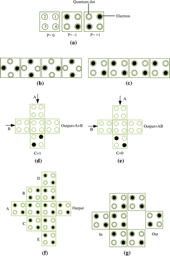
Cells are the elementary entities of QCA based circuit and they are usually constituted of four quantum dots positioned at the corners of a square pattern. Each cell is charged with two supplementary electrons which channel from one low potential state to another across a high potential direction and a back plane voltage switches the cell occupancy. The electrons will be located in transversely to each other owing to reciprocal repulsive electrostatic power, possessing the utmost distance between them. A remote cell may be in one of two corresponding energy positions. These positions are called cell polarizations P = +1.00 and P = −1.00 as shown in Figure (a) p = 0 denotes an unpolarized cell which covers no information. A cell polarization P is −1 if the electrons are involved the locus 2 and 4, in the same way, a cell polarization P is +1 if electrons are involved the position 1 and 3. The cell polarization equation (Lent et al., Citation1993) is presented below.(1)
(1)
Figure 1. QCA cell with diverse polarization (a), QCA 45° wire (b), 90 wire (c), Majority voter function as 2-input OR gate (d), 2-input AND gate (e), 5-input majority gate (f) and robust inverter (g).
where, the charge at dot i denoted by ρi
2.2. QCA wire
QCA wire encompasses of series of cells where the cells are united one after another (Abdullah-Al-Shafi, Citation2016a; Abu Arqub, Citation2015; Islam et al., Citation2016). QCA wire is employed to transfer signal from one position to another in a circuit. Logical charges are moved from cell to cell because of the coulomb contacts. There are two modes of alignments in a QCA wire namely binary wire and inverter chain. QCA wires can be either originated up of 45o cells or 90o cells as shown in Figure (b) and (c). In case of inverter, if two cells point at 45o with regard to each other their contact will be reverse and for that, these cells are mostly employed for coplanar wire crossings.
Binary wire transfers signal with similar polarity from one place to another, while inverter chain reverses the input cell polarity when odd figures of cells are employed in it.
2.3. Majority gates
Majority gate is assembled of five QCA cells; a central cell, one output, and three inputs. Polarity of the middle cell, as identified as device cell is imposed, by the coulomb repulsion to be equivalent to the output cell. The device cell at the center of the gate has its least energy when it accepts the polarization of the majority of the three input cells since this is the formation where the repulsion among the electrons in the three inputs cells and the electrons in the device cell is the lowest. So, an arrangement of inverter and majority voter is appropriate to construct an extensive logic set for scheming any circuit.
Majority voter can operate as AND or OR logic gate depending on the static polarity of the third input of the majority voter presented in Figure (d) and (e). Logical 2-input AND and 2-input OR functions can be executed using majority voter by putting one input cell to binary “0” and “1”, subsequently. The logical equation of the 2-input majority gate can be stated as follows.(2)
(2)
The satisfying attainment of realizing a 3-input majority voter with five QCA cells inspired the analysts to hypothesize an inventive configuration for 5-input majority voter. Later, a specific layer (Abdullah-Al-Shafi & Bahar, Citation2016b) 5-input majority voter utilizing ten cells executed in a precise cell layout which is displays in Figure (f). The logic equation of the 5-input majority voter can be expressed as follows.(3)
(3)
2.4. QCA inverter
The inverter is a pattern of cells that reverse the input topology from one logic to another. Usually, two categories of inverter are applied (Abdullah-Al-Shafi, Citation2016b) that has been operated for the realization of several structures as an essential cell (Abdullah-Al-Shafi & Bahar, Citation2016c; Islam et al., Citation2015). The inverter can be designed by fixing QCA cells at 45° position (Abdullah-Al-Shafi & Bahar, Citation2016b) as appeared in Figure (g) which is potent and mostly used in circuit design. The logic values 0 and 1 transformed to 1 and 0 because of electrostatic repulsion.
2.5. QCA clocking mechanism
To form more complicated QCA devices, the location of QCA cell is not only essential also needs to coordinate the information, so that evade having a signal extending a logic gate and proliferating before the other inputs move the gate. This specific characteristic is particularly imperative in QCA circuits, ensuring its accurate function and this aspect are attained by QCA clock. The clock is an electrical region that switches the channeling barriers within a cell, therefore retaining control when a cell may or may not be polarized. QCA clocking is produced of four periods lagging by π/2 (Hennessy & Lent, Citation2001) as shown in Figure which generates an innovative way to conceive nano-circuit distinct from the regular CMOS circuits (Walus, Dysart, Jullien, & Budiman, Citation2004). In each region, a certain potential can adjust the barriers between the dots and the organization of clock zones allows a group of QCA cells to construct a particular calculation and then its positions are stationary and its outputs can be applied as inputs to the following clock zone.
Figure 2. QCA Four stage clocking (a) and signal for clocking zones (b).
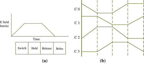
Switch period: the barrier between dots of QCA cell is elevated and the dots are motivated by the electron of its adjoining as well as electron begins channeling between dots. Thus, the cell turns into polarized.
Hold period: cell barrier stays high and electron cannot channel between dots and the cell keep its existing position.
Release period: barrier between dots are decreased, the electron can channel within dots and cell comes to be unpolarized.
Relax period: barrier remains at lowered and cell stays in unpolarized position.
3. Proposed QCA outlines
An assay is fulfilled to acquire the required devices and selected to realize the suggested design. The composition level is permitted applying a number of approximate simulators as the nonlinear approximation methods and bistable simulation device. However, these approximate do not develop the specified measures because these methods are iterative. In time, the QCA Designer is preferred simulation tool (Walus et al., Citation2004). The Bistable simulation tool has been occupied in the simulation interface between cells, clearly, the contact force linking two cells decomposes contrariwise with the fifth power of the length untangling them. During this estimation, not all the cells impact are counted and cell within the radius of R are being measured. For cell i, the scientifical pattern is depicted by the following Hamiltonian.
(4)
(4)
where Pj is the polarization for cell j, is the kink energy between the cells (i and j) and ϒ is the channeling energy. For every cell i, the amount of the hamiltonian is over all cells (viz., j) in its radius of effect R. The Jacobi algorithm has been utilized to obtain the eigenvectors and eigenvalues of the Hamiltonian. At the layout level, small QCA block is designed and simulated for analysis its precision. Later these QCA blocks are unified together through QCA wire to manage the proposed composition. Finally, the consistency of the design is surveyed by the QCA Designer. The simulation outcome the essential waveform for the logical circuit and during simulation, it created few criterion that contains default standards as the cell size, layer separation, relative permittivity, samples number etc.
3.1. 2:4 decoder
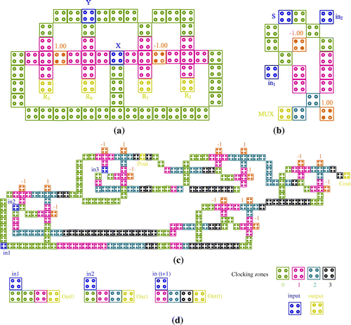
The proposed 2:4 decoder uses four-periods clocking zones in QCA. The QCA layout of the proposed decoder circuit is shown in Figure (a) using four majority voters and three inverters. The logical expression of 2:4 decoder is described as. The input signals (X, Y) are decoded as:(5)
(5)
(6)
(6)
(7)
(7)
(8)
(8)
Figure 3. QCA outline of proposed 2:4 decoder (a), 2:1 multiplexer (b), nano communication circuit (c) and D flip-flop (d).
3.2. 2:1 Multiplexer
The proposed 2:1 multiplexer has two inputs in1 and in2, one address line s and single output state. If address line s = 0, input in1 is selected, and when s = 1, input in2 performs at the output. The majority voter illustration of the function is as followed.(9)
(9)
3.3. Nano communication circuit in QCA
The proposed complex circuit is designed using a parity checker and parity generator function. Parity initiator or generator selects bit data as an input signal and produces parity bit. Through transmission channel, the bit data and generated parity bit are directed to parity checker. Then the bits are verified by checker circuit which was covered within the message for fault detection. If the parity bit is not odd, then a fault is arises all through the transmission. The QCA layout of the proposed circuit is presented in Figure (c).
3.4. Reversible D flip-flop
The inputs of reversible D flip-flop is defined as in (t + 1), in2, in1 and the corresponding outputs lines are out (t), out, out1. The input arrangements from “000” to “111” allow one to one correlation with the outputs. The logical expression can be derived as in (t + 1) = out (t), in2 = out, and in1 = out1. The straight interactions between the output and input cells are presented in Figure (d). The proposed figure shows one to one correlation so only with certain delay, the inputs should shift the outputs unaffected.
4. Simulation results and performance analysis
Simulation results functionally have been obtained using the QCA Designer (Walus et al., Citation2004) that is a popular engine for QCA circuits. The simulation results of the proposed outlines are shown in Figure . The used criterions for the simulation are as follows: samples number: 12,800, convergence tolerance 0.001, radius of effect (bistable and coherence) 65 and 80 nm, threshold (lower and upper) −0.50 and 0.50, scale of cell is 18 nm, separation of layer is 11.50. The decoder circuit involves only 83 cells and covering an extent of 0.08 μm2, the multiplexer involves of 18 cells and covering an extent of 0.02 μm2, the flip-flop layout involves only 9 cells and covering an extent of 0.02 μm2 and the nano communication circuit involves of 275 QCA cells with an extent of 0.41 μm2. It is very essential to create an operationally firm layout in QCA and there are certain concerns realized into account to rise the design stability. When building models in QCA, a substantial attempt should be made to maintain the wire length in a specified clocking region to a minimum.
Figure 4. Simulation results of 2–4 decoder (a), 2-1 multiplexer (b), nano communication circuit (c) and D flip-flop (d).
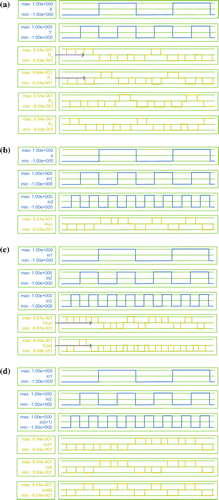
In Figure (a), the input X and Y to the output signals of R3, R2, R1, R0 in this unit goes through four clock levels, so the delay is an entire clock cycle. Hence the output, R3, R2, R1, R0 is presented single clock cycles after X and Y have been affected. The output value of R0 is up when the input X = Y = 0 if the input is X = Y = 0 then the output value of R1 is low. The starting position of the output line R0 and R1 is shown by arrows in the figure.
In the multiplexer outline, input in1, in2 and address line s is 01010101, 00110011 and 00001111 correspondingly. The result is 01010011 as presented in Figure (b). From the figure, it can be studied that for the primary four clock cycles address line is zero the output is following the input in1 for these four cycles, and when address line is 1 for succeeding four clock cycles, the result is following input in2.
Figure (c) explains the nano communication architecture, when the input bits to the transmitter are in1 = in2 = in3 = 0, then the corresponding output will be Pout = 1. In the recipient section, if the inputs are in1 = in2 = in3 = 0, the output will be Cout = 0. Similarly, others bit streams can be formed. The output Pout and Cout perform after the second cycle as indicated by arrows in the figure.
The outcome of proposed reversible D flip-flop is presented in figure (d) where the outputs out = out(1) = out(t) is low if all the inputs in1, in2 and in (t + 1) are low. Inputs are functional at “0” clocking region and outcome are gained at following clock zone so, the outcome is consistent and firm.
The layout intricacies in terms of the majority voters number, QCA cells, circuit thickness and the clocking zones applied to devise the circuits as presented in Table .
Table 1. Complexity study of proposed circuits
The designed multiplexer is compared with previous outlines in terms of area, cell number, and delay. The effects are presented in Table . The proposed circuit has 17.39 and 62.50% enhancement in terms of QCA cell and delay compared with (Sen & Goswami, Citation2015) and 29.63 and 75.00% enhancement in terms of cell and delay correspondingly, comparative to the outline proposed in (Roohi et al., Citation2011). Likewise, other enhancements are showed in Figure (a). The assessment in Table presents that the proposed multiplexer outline has minimal cell count with better device thickness and is relatively faster than existing outlines.
Table 2. Performance analysis of proposed multiplexer with existing outlines
Figure 5. A comparative study of proposed multiplexer (a), decoder (b) and nano communication circuit (c).
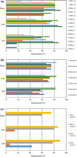
The decoder is assessed with previous outlines in terms of area, cell number and delay and the results are presented in Table . The proposed circuit has enhancements of 56.94, 71.91 and 75% in terms of cell, area and clock delay correspondingly, comparative to the outline proposed in (Vetteth et al., Citation2002). Likewise, other enhancements are showed in Figure (b). The assessment in Table presents that the proposed decoder outline has better performance than existing outlines.
Table 3. Performance analysis of proposed decoder with existing outlines
Table presents the comparison study of the proposed nano communication circuit with existing designs. The circuit attains 6.14 and 14.40% improvements in terms of cell and area as compared with (Das & De, Citation2016) and other enhancements are illustrated in Figure (c).
Table 4. Performance analysis of nano communication circuit with existing layouts
The overall enhancements of proposed decoder, multiplexer, and nano communication circuit are demonstrated in Figure , correspondingly.
5. Power consumption of the proposed outlines
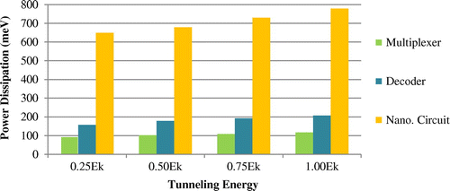
The dissipation of power by each QCA cell in a circuit is identical (Abdullah-Al-Shafi & Bahar, Citation2016b, Citation2016c). Therefore, in a range of connected QCA cells, the total dispelled power can be projected by adding the dispelled power of each cell within the range. The circuit’s power consumption is reliant on the logic gates operated in constructing the circuit. Apply a larger quantity of logic gates, involves larger power dissipation by the circuits. The dispelled energy of the circuit is the total of the power dissipated by all the majority voters, inverters, and the range of QCA cells. This paper, mathematical analysis of Hamming distance based assessment of power dissipation is applied to achieve the power dissipation of the proposed circuits. The assessment is achieved using the similar temperature (i.e. T = 2.0 K) and the similar channeling energies (i.e. 0.25Ek, 0.75Ek, etc.). It has been described (Liu et al., Citation2012) that for a shift in the Hamming distance between inputs to the circuit, the energy dispelled will also be differ.
In the case of the inverter, 1 → 1 or 0 → 0 input switching means Hamming distance “0”, and the inverter has dispelled the power of 0.8 meV at γ = 0.25Ek and 2.7 meV at γ = 0.5Ek. A ceiling Hamming distance of “3” is measured for the majority voter for 000 → 111 input switching, that affects the ceiling dissipated the energy of 41.0 meV by the majority voter at γ = 0.25Ek and 41.2 meV at γ = 0.5Ek. Correspondingly, dissipation of power by the majority voter and inverter for several Hamming distances was testified in. The QCA design of the proposed decoder consists of three inverters and four majority gates. Each of these majority voters has one stable input polarization. Therefore, the Hamming distance for these majority voters is measured to be “2”, respectively. For maximum energy dissipation, Hamming distance “1” is measured for each of the inverters. Applying the Hamming distances related to the input to logic gates and counting the QCA arrays perform in decoder as shown in Figure (a), the power dissipation of the proposed decoder is analyzed. The results are shown in Table . An equal method is applied for figuring the power dissipation by the multiplexer and nano communication circuit and the outcomes are denoted in Table . Table illustrates that the power dissipated by the decoder at γ = 0.25Ek is 156.4 meV and at γ = 1.0Ek, it is 206.8 meV. Similarly, dissipated power by the other outlines is formed which is presented in Table . These outcomes show that all the circuits dissipate very little heat energy. The results are also outlined in Figure .
Table 5. Power dissipation of the proposed circuits
Figure 6. Power depletion of the proposed architecture.
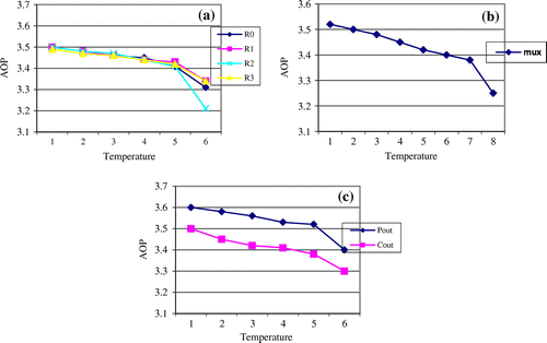
The average output polarization (AOP) of any cell of the QCA circuit is decreased by enhancing the temperature (Abdullah-Al-Shafi & Bahar, Citation2016b). The outcome of temperature on the AOP of the urged circuits is presented in Figure . The AOP of the output of the proposed decoder is slowly lessened, up to a temperature of T = 5 K. Multiplexer work competently between 1 and 7 K. Similarly, the nano communication circuit work proficiently between 1 and 5 K.
Figure 7. Temperature effect on AOP of the proposed multiplexer (a), decoder (b) and nano communication circuit (c).
6. Conclusion
QCA is a new and ultra-high speed nanotechnology. In this paper, novel architecture of multiplexer, decoder, D flip-flop and nano-communication circuits have been proposed, which are faster and more efficient than existing layouts. The proposed QCA circuit’s excelled the existing one in terms of cell complexity, area, wire crossing and latency. Moreover, the proposed circuits dissipate low heat, presents that the proposed QCA structures are appropriate for applying complex logic circuits. In future, the high robustness of reversible/ irreversible logic can be implemented using the proposed structures. These can be most commonly utilized to design faster, denser and fault-tolerant circuits.
Funding
The authors received no direct funding for this research.
Additional information
Notes on contributors
Md. Abdullah-Al-Shafi
Md. Abdullah-Al-Shafi received his BSc (Engg.) in Information and Communication Technology in 2015. Currently pursuing an MS in Information Technology (IT) in Institute of Information Technology (IIT), University of Dhaka, Bangladesh. He has more than 15 research publications in renowned international journals and conference. His research area includes Distributed Computing, Quantum-dot Cellular Automation, Intelligent System and Wireless Sensor Network.
Ali Newaz Bahar
Ali Newaz Bahar had been working as Assistant Professor in the Department of Information and Communication Technology (ICT), Mawlana Bhashani Science and Technology University, Bangladesh. He has more than 50 research publications.
Firdous Ahmad
Mr Firdous Ahmad received his MPhil degree award in QCA from Kashmir University, Hazratbal Srinagar, India in 2014. He is currently a PhD research scholar of Nanotechnology Laboratory from Kashmir University, Hazratbal Srinagar, India.
Kawsar Ahmed
Mr Kawsar Ahmed received his BSc and MSc Engineering Degree in Information and Communication Technology (ICT) at Mawlana Bhashani Science and Technology University, Tangail, Bangladesh. Currently, he is serving as an Assistant Professor at the same department.
Related Research Data
References
- Abdullah-Al-Shafi, M. (2016a). Analysis of fredkin logic circuit in nanotechnology: An efficient approach. International Journal of Hybrid Information Technology, 9, 371–380.10.14257/ijhit
- Abdullah-Al-Shafi, M. (2016b). Synthesis of peres and R logic circuits in nanoscopic scale. Communications on Applied Electronics, 4, 20–25.10.5120/cae2016652004
- Abdullah-Al-Shafi, M., & Bahar, A. N. (2016a). QCA: An effective approach to implement logic circuit in nanoscale. In Presented at the 5th International Conference on Informatics, Electronics & Vision (ICIEV), International Conference on, IEEE (pp. 620–624). Dhaka.
- Abdullah-Al-Shafi, M., & Bahar, A. N. (2016b). Optimized design and performance analysis of novel comparator and full adder in nanoscale. Cogent Engineering, 3, 1237864.
- Abdullah-Al-Shafi, M., & Bahar, A. N. (2016c). Novel binary to gray code converters in QCA with power dissipation analysis. International Journal of Multimedia and Ubiquitous Engineering, 11, 379–396.10.14257/ijmue
- Arqub, O. A. (2015). Adaptation of reproducing kernel algorithm for solving fuzzy Fredholm-Volterra integrodifferential equations. Neural Computing & Applications. doi:10.1007/s00521-015-x
- Arqub, O. A., Al-Smadi, M., Momani, S., & Hayat, T. (2016). Application of reproducing kernel algorithm for solving second-order, two-point fuzzy boundary value problems. Soft Computing. doi:10.1007/s00500-016-2262-3
- Askari, M., Taghizadeh, M., & Farhad, K. (2008). Digital design using quantum-dot cellular automata (a nanotechnology method). In Proceedings of the IEEE international conference on computer and communication engineering (ICCCE 2008) (pp. 952–955).
- Bahar, A. N., Abdullah-Al-Shafi, M., & Bhuiyan, M. M. R. (2017). Designing efficient QCA even parity generator circuits with power dissipation analysis. Alexandria Engineering Journal. doi:10.1016/j.aej.2017.02.002 ( Accepted).
- Compano, R., Molenkamp, L., & Paul, D. J. (2000). Roadmap for Nanoelectronics. European Commission IST Programme, Future and Emerging Technologies.
- Das, J. C., & De, D. (2016). Quantum-dot cellular automata based reversible low power parity generator and parity checker design for nanocommunication. Frontiers of Information Technology & Electronic Engineering, 17, 224–236.
- Debnath, B., Das, J. C., & De, D. (2016). Reversible logic-based image steganography using quantum dot cellular automata for secure nanocommunication. IET Circuits, Devices & Systems, 11, 1–10.
- Debnath, B., Das, J. C., De, D., & Sadhu, T. (2016, March). A novel low power nanoscale reversible decoder using quantum-dot cellular automata for nanocommunication. In Devices, circuits and systems (ICDCS), 2016 3rd International conference on IEEE (pp. 220–224).
- Hashemi, S., Azghadi, M., & Zakerolhosseini, A. (2008). A novel QCA multiplexer design. In Proceedings of the IEEE international symposium on telecommunications (pp. 692–696).
- Henderson, S. C., Johnson, E. W., Janulis, J. R., & Tougaw, P. D. (2004). Incorporating standard CMOS design process methodologies into the QCA logic design process. IEEE Transactions On Nanotechnology, 3, 2–9.10.1109/TNANO.2003.820506
- Hennessy, K., & Lent, C. S. (2001). Clocking of molecular quantum-dot cellular automata. Journal of Vacuum Science & Technology B: Microelectronics and Nanometer Structures, 19, 1752–1755.10.1116/1.1394729
- Islam, M. S., Shafi, M. A., & Bahar, A. N. (2016). A New Approach of Presenting Universal Reversible Gate in Nanoscale. International Journal of Computer Applications, 134, 1–5.10.5120/ijca2016910208
- Islam, S., Shafi, M. A., & Bahar, A. N. (2015). Implementation of binary to gray code converters in quantum dot cellular automata. Journal of Today's Ideas–Tomorrow's Technologies, 3, 145–160.10.15415/jotitt.2015
- Kianpour, M., & Sabbaghi-Nadooshan, R. (2011, December). A novel modular decoder implementation in quantum-dot cellular automata (QCA). In Nanoscience, technology and societal implications (NSTSI), 2011, International conference on IEEE (pp. 1–5).
- Kim, K., Wu, K., & Karri, R. (2007). The robust QCA adder designs using composable QCA building blocks. IEEE Transactions on Computer-Aided Design of Integrated Circuits and Systems, 26, 76–183.
- Lent, C. S., Tougaw, P. D., Porod, W., & Bernstein, G. H. (1993). Quantum cellular automata. Nanotechnology, 4, 49.10.1088/0957-4484/4/1/004
- Liu, W., Srivastava, S., Lu, L., O’Neill, M., & Swartzlander, E. E. (2012). Are QCA cryptographic circuits resistant to power analysis attack? IEEE Transactions on Nanotechnology, 11, 1239–1251.
- Makanda, K., & Jeon, J. C. (2014). Combinational Circuit Design Based on Quantum-Dot Cellular Automata. International Journal of Control and Automation, 7, 369–378.
- Mardiris, V. A., & Karafyllidis, I. G. (2010). Design and simulation of modular 2n to 1 quantum-dot cellular automata (QCA) multiplexers. International Journal of Circuit Theory and Applications, 38, 771–785.
- Mardiris, V., Mizas, C. H., Fragidis, L., & Chatzis, V. (2008). Design and simulation of a QCA 2 to 1 multiplexer. In Proceedings of the 12th WSEAS International Conference on Computers (pp. 572–576).
- Roohi, A., DeMara, R., & Khoshavi, N. (2015). Design and evaluation of an ultra-area-efficient fault-tolerant QCA full adder. Microelectronics Journal, 46, 531–542.10.1016/j.mejo.2015.03.023
- Roohi, A., Khademolhosseini, H., Sayedsalehi, S., & Navi, K. (2011). A novel architecture for quantum-dot cellular automata multiplexer. International Journal of Computer Science Issues, 8, 55–60.
- Sabbaghi-Nadooshan, R., & Kianpour, M. (2013). A novel QCA implementation of MUX-based universal shift register. Journal of Computational Electronics, 13, 1–13.
- Sen, B., Dutta, M., Goswami, M., & Sikdar, B. K. (2014). Modular design of testable reversible ALU by QCA multiplexer with increase in programmability. Microelectronics Journal, 45, 1522–1532.10.1016/j.mejo.2014.08.012
- Sen, B., Dutta, M., Saran, D., & Sikdar, B. K. (2012). An efficient multiplexer in quantum-dot cellular automata. Progress in VLSI design and test. Lecture notes in computer science (Vol. 7373, pp. 350–351). Berlin: Springer.10.1007/978-3-642-31494-0
- Sen, B., Goswami, M., Mazumdar, S., & Sikdar, B. K. (2015). Towards modular design of reliable quantum-dot cellular automata logic circuit using multiplexers. Computers & Electrical Engineering, 45, 42–54.10.1016/j.compeleceng.2015.05.001
- Sen, B., Nag, A., De, A., & Sikdar, B. K. (2015). Towards the hierarchical design of multilayer QCA logic circuit. Journal of Computational Science, 11, 233–244.10.1016/j.jocs.2015.09.010
- Shafi, A., Bahar, A. N., & Islam, M. S. (2015). A quantitative approach of reversible logic gates in QCA. Journal of Communications Technology, Electronics and Computer Science, 3, 22–26.10.22385/jctecs.v3i0.33
- Silva, D. S., Sardinha, L. H., Vieira, M. A., Vieira, L. F., & Neto, O. P. V. (2015). Robust serial nanocommunication with QCA. IEEE Transactions on Nanotechnology, 14, 464–472.10.1109/TNANO.2015.2407696
- Singh, S., Pandey, S., & Wairya, S. (2016). Modular design of 2 n: 1 quantum dot cellular automata multiplexers and its application, via clock zone based crossover. International Journal of Modern Education and Computer Science, 8, 41–52.10.5815/ijmecs
- Teodósio, T., & Sousa, L. (2007). QCA-LG: A tool for the automatic layout generation of QCA combinational circuits. In Proceedings of the 25th IEEE norchip conference (pp. 1–5).
- Vetteth, A., Walus, K., Dimitrov, V. S., & Jullien, G. A. (2002, September). Quantum-dot cellular automata carry-look-ahead adder and barrel shifter. In IEEE emerging telecommunications technologies conference (pp. 2–4).
- Walus, K., Dysart, T. J., Jullien, G. A., & Budiman, R. A. (2004). QCA designer: A rapid design and simulation tool for quantum-dot cellular automata. IEEE Transactions On Nanotechnology, 3, 26–31.10.1109/TNANO.2003.820815
- Zhou, R., Xia, X., Wang, F., Shi, Y., & Liao, H. (2012). A logic circuit design of 2-4 decoder using quantum cellular automata. Journal of Computational Information Systems, 8, 3463–3469.