
 ?Mathematical formulae have been encoded as MathML and are displayed in this HTML version using MathJax in order to improve their display. Uncheck the box to turn MathJax off. This feature requires Javascript. Click on a formula to zoom.
Abstract
By the gradual increasing of the attribute size and energy utilization in VLSI chips the component of energy depleted owing to information forfeiture in irreversible valuations will turn into a crucial drawback in the future. Nano components, particularly quantum-dot cellular automata (QCA), have attained extensive interests for their foremost aspects as contrasted to the typical complementary metal oxide semiconductor (CMOS) circuits. QCA, especially due to its substantial diminution in latency, dimension, and energy utilization of circuits, is counted as a latent substitute for the CMOS technology. In this study, a design of RS flip-flop circuit in QCA is proposed. We review an approach for simplified outline of QCA circuits such that the dimensions and energy depletion are substantively decreased. The designed circuit is carried out using single layer and does not involve any rotated cells which particularly expand the fabrication of the outline. The proposed design is simulated with QCADesigner and energy utilization is estimated using QCAPro tool which is a widespread simulation tool. Assessments specify that the outlined structure significantly reduces the number of cells, extent, and latency and depletes very low power which simplifies the complete circuit manufacture and implementation.
Public Interest Statement
Quantum-dot Cellular Automata is an exclusive computation approach which is founded on semiconductor substantial. This standpoint study depicts a superior circuit design of set-reset (RS) flip-flop. The key significance of the proposed circuit is designing without wire-crossing as well as consumed less number of cell and space. Moreover, the layout is considerably lessened in terms of cell intricacy and latency. The proposed design attained complete improvement compared to earlier outlines. Power depletion by the layout specifies that the design dissipated very low energy. The proposed circuit can be used for counter design, register and shift register implementation, frequency counter and computers.
1. Introduction
In current years, because of the advent of crucial constrictions against substantial scalability of the complementary metal oxide semiconductor (CMOS) outline, several deficiencies and difficulties have been classified. A few of these problems inherent to this outline are short channel influences and extreme leakage power utilization (Liu, Lu, O’Neill, & Swartzlander, Citation2014; Roohi, Khademolhosseini, Sayedsalehi, & Navi, Citation2014). A number of substitute technologies (Abdullah-Al-Shafi & Bahar, Citation2016a) as carbon nanotube field effect transistor, nanowire-based transistor and quantum-dot cellular automata (QCA) (Lent, Tougaw, Porod, & Bernstein, Citation1993) have previously been recommended for the CMOS outline to solve these shortcomings. Among the substitute resolutions, QCA has concerned far more consideration as it has presented particular device thickness, rapid operation and extremely low energy (Abdullah-Al-Shafi, Citation2016a; Abdullah-Al-Shafi & Bahar, Citation2016a; Islam, Shafi, & Bahar, Citation2016). In every QCA cell, two arrangements subsist that can program the binary information. The majority voter performs a considerable part in the circuits assembled based on the QCA technology (Abdullah-Al-Shafi, Citation2016b; Abdullah-Al-Shafi & Bahar, Citation2016a; Al Shafi, Bahar, & Islam, Citation2015; Islam, Shafi, & Bahar, Citation2015). With the inverter and majority voter permits manufacturers to form any functions in QCA technology (Abdullah-Al-Shafi, Aneek, & Bahar, Citation2017; Abdullah-Al-Shafi & Bahar, Citation2017; Abdullah-Al-Shafi, Bahar, Ahmad, & Ahmed, Citation2017; Abdullah-Al-Shafi, Bahar, Ahmad, Bhuiyan, & Ahmed, Citation2017; Abdullah-Al-Shafi et al., Citationin press; Bahar, Uddin, Abdullah-Al-Shafi, Bhuiyan, & Ahmed, Citation2017; Biswas, Bahar, Habib, & Abdullah-Al-Shafi, Citation2017; Hassan et al., Citation2017). Energy utilization is certainly the foremost affair in current VLSI circuits. Because of the ever growing requirements for convenient electronic structures and the inconsistent progress of the semiconductor and battery production businesses, expanding the functioning time between every single battery charge has to turn into incredibly curtail. Moreover, the inconsistent scaling of the dimension of transistors and power source voltage has directed to several deficiencies (Abdullah-Al-Shafi, Citation2016a; Abdullah-Al-Shafi et al., Citation2017; Liu et al., Citation2014) forming hot spots in CMOS microchip. Accordingly, separate computational patterns through evolving nanotechnologies, concentrate on minimal power depletion and radically small extent should be measured. Landauer showed that each one bit of information forfeit in an irreversible assessment leads to kBTln2 joules depletion of heat energy, where kB is denoted as Boltzmann constant and T is the room temperature (Landauer, Citation1961). Though the depletion of the existing CMOS circuits is far excessive than kBTln2, in the forthcoming with eventual scaling of attribute size and power utilization based on evolving technologies, this hypothetical constraint may turn into a main restriction (Sen, Dutta, Some, & Sikdar, Citation2014). In this study, an enhanced Reset Set (RS) flip-flop is presented, which in contrast with the former outlines involve the minimal number of QCA cells and extent. As well the proposed design depletes very low energy. The remainder of this study is prepared as follows: Section 2 concisely analyses the QCA fundamental properties. Section 3 illustrates the proposed QCA design. The simulation outcomes and assessments are organized in Section 4 and lastly, Section 5 deduces the study.
2. A concise study of the QCA technology
2.1. QCA fundamentals
Each four-sided QCA cell contains four quantum dots employed by a pair of electrons. Because of the coulomb revulsion concerning two electrons, they will be sited at transversely reverse places. The parameter P, presented by Equation (1), is described to determine this placement, where the value ρi is the chance of the existence of an electron in quantum-dot i (Tougaw & Lent, Citation1996).(1)
(1)
Because of a higher inter-cell potential, the electrons cannot channel between two cells. Though they can channel between adjacent dots. There present two arrangements in every cell with the polarizations labeled as +1 and −1 which are signified by binary values of 1 and 0 (Tougaw & Lent, Citation1996). Once a bit switches from “0” to “1” and vice versa, no authentic charging and discharging of capacitors appear as in CMOS. Besides, conduction of logic from one cell to another is achieved by the interface of electrons in adjoining cells and there is no movement of current between QCA cells. Hence, there is no energy depletion through the state changeover and propagation in QCA. Thus, QCA depletes very little power as contrasted to the CMOS circuits. In QCA, a wire is comprised of an arrangement of QCA simple cells that circulates an input value to the target cell by the columbic revulsions concerning the electrons of the successive cells. The wires are comprehended in two categories, including 45-degree or 90-degree cells (Abdullah-Al-Shafi, Citation2016a, Citation2016b; Abdullah-Al-Shafi & Bahar, Citation2016). The major QCA logic gates are the three input majority voters and inverter which are presented in Figure (b)–(d), correspondingly.
Figure 1. QCA logic (a) Cells indicating logic “0” and logic “1”, (b) Simple inverter, (c) QCA robust inverter and (d) Three-input majority voter.
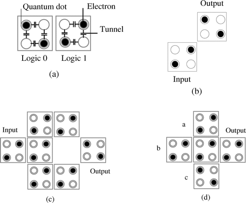
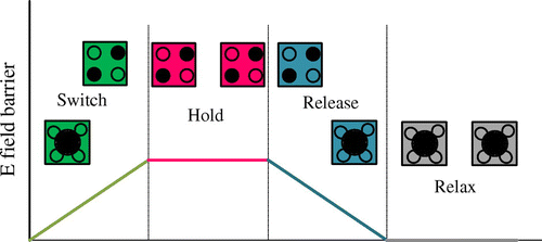
The arrangement of the inverter and majority voters specifies a comprehensive gate identified the minority gate. As per the type of the QCA formation, the circuits in QCA are generally devised based on the inverter and majority gates (Tougaw & Lent, Citation1994). A clock is necessary to provide the potential gain for cells and manage the data flow in QCA circuits. It is attained by scheming the potential block energies between adjoining quantum-dots. A four stage clocking arrangement is applied to specify the circulation of data over the logic circuits (Abdullah-Al-Shafi & Bahar, Citation2016a, 2016b). Specified a number of potential blocks, the energy stages can be outlined in four clocking regions with π/2 phase variance (Hennessy & Lent, Citation2001). This clocking structure containing switch, hold, release and relax periods is explained in Figure .
Figure 2. Four clocking zones in QCA outline.
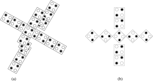
QCA Wire crossing can be realized by tree methodologies including coplanar and multi-layer (Shin, Jeon, & Yoo, Citation2013). In the first method, present in Figure (a), to transfer the accurate values in every single wire, multi-layer outline should be utilized. In this technique, a wire is applied in one layer and another wire is applied in a cross position in the other layer. The next method, presented in Figure (b), to transfer the accurate values in every single wire, a coplanar technique is applied. For this procedure, one of two wires is applied with 45-degree cells and the other wire is applied with 90-degree cells.
Figure 3. QCA multi-layer wire crossing (a) and coplanar approach (b).
2.2. Stable values concern in QCA technology
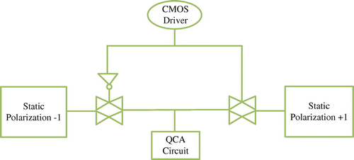
There are usually two systems for recognizing the stable values essential in a QCA cell. First one is a QCA system that allocates the essential uniform polarization, whereas the second method, utilized the dot-level operation of cells inside the QCA circuit (Walus & Jullien, Citation2006).
The design of stable input driver in the QCA circuits on external inputs is presented in Figure . A separate extent must be counted to affect the values in the circuits. In practical circumstances, an extra space and supplementary arrangement and channeling over another level to distribute the preferred value into stable input cells are essential to insert arbitrary values into stable cells.
Figure 4. The construction of input driver.
2.3. QCA circuits construction
QCA circuits can be constructed by several approaches comprising, semiconductor, molecular formations, nanomagnetic and metal-island. QCA semiconductor approach can be manufactured with electron beam lithographically outlined on the GaAs/ALGas heterostructure substance as presented in (Smith et al., Citation2003). The metal-island organization can be formulated on a silicon wafer. The formulation of a cell with aluminum metallic dots and expansions of this sort of QCA cell to a wire have been reviewed in (Orlov, Amlani, Bernstein, Lent, & Snider, Citation1997). Nanomagnetic QCA cell construction has been presented in (Cowburn & Welland, Citation2000). Assembly and presentation of a QCA cell on an ion-implanted phosphorus-doped silicon has been reported in (Mitic et al., Citation2006). Various constituents like graphene (Wang & Lieberman, Citation2004) can be used to realize the molecular method. It can be perceived in recent times that there is a notable possibility for improvement in the construction of QCA based nanocircuits.
3. Proposed QCA circuit
The SR flip-flop is measured as one of the utmost elementary sequential logic circuits. This plain circuit is mainly a single-bit memory bistable design which has two fixed inputs, one that will “SET” the circuit and another that will “RESET” the circuit as presented in Figure .
Figure 5. Basic SR flip-flop circuit.
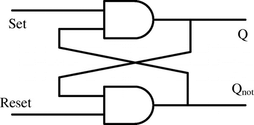
The SR account stands for “Set-Reset”. The reset state resets the circuit back to its initial position with a result Q that will be either at a logic stage “0” or logic “1” rest on this set/reset state.
The majority gate illustration of the proposed circuit is presented in Figure (a) and the equation is given to as follows.(2)
(2)
Figure 6. Proposed QCA Outline (a) Schematic diagram and (b) QCA design.
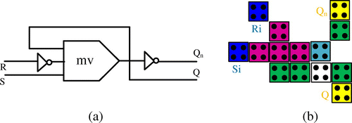
The QCA presentation of the proposed circuit is shown in Figure (b) where Ri and Si are the input and Qn and Q denoted as output. The central loop of the circuit has single delay; however, at the output, Q is accessible 2.75 clocking levels after R and S have been affected. The proposed layout is confirmed with QCADesigner ver. 2.0.3, with the succeeding factors for a bistable approximation: Cell size = 18 nm, Number of samples = 20,000, Radius of effect = 90 nm, Clock high = 9.8e-22J, Clock low = 3.8e−23J, Clock amplitude factor = 2, Relative permittivity = 12.90, Layer separation = 11.5 nm, Maximum Iterations per sample = 100 and Convergence tolerance = 0.001. For coherence vector simulation the succeeding factors are: Temperature = 1.00 K, Relaxation time = 1.0e-15s, Time step = 1.0e-16s, Overall simulation time = 7e−11s, Clock shift = 0, Radius of effect = 80 nm, Clock low = 3.8e−23 J, Clock amplitude factor = 2 and Relative permittivity = 12.90.
4. Results study and assessments
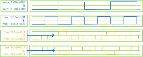
This section, the outlined circuit is simulated with the QCADesigner tool (Walus, Dysart, Jullien, & Budiman, Citation2004). Simulation result of the flip-flop is shown in figure and from the result, it is clear that the result is attained after 2.75 delay. The delay is indicated with a blue arrow.
Figure 7. Simulated outcome for proposed RS flip-flop.
The outlined circuit is attained with 2 fixed inputs, 1 majority gate, 14 cells with extent of 0.01 μm2 and 4 clocking zones that is considerably enriched than existing layout.
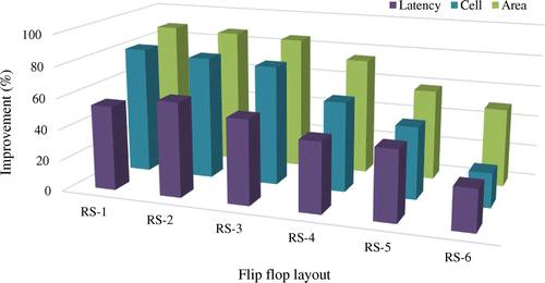
4.1. Evaluation of proposed and previous RS flip flop
The evaluation is accomplished in terms of the number of applied cells, clock phase, and used space (Abdullah-Al-Shafi & Bahar, Citation2017; Abdullah-Al-Shafi et al., Citation2017). The layout in (Vetteth, Walus, & Dimitrov, Citation2003) consumes 76 QCA cell with a dimension of 0.09 μm2 and latency 6. Proposed flip-flop acquired an improvement of 81.58, 88.89 and 54.17% in terms of used cell, extent and delay, correspondingly. As well the proposed circuit do not use any rotated cell.
Comparing with (Rezaei, Citation2017), the outlined circuit attained an enhancement of 46.16, 58.33, and 45.00%, respectively. In the same way, other estimation is organized in Table and improvement analysis with earlier flip-flop is shown in Figure .
Table 1. Assessment study of the proposed RS flip-flop with earlier designs
Figure 8. An improvement study of outlined flip flop with previous layouts.
4.2. Energy depletion of the proposed layout
The energy depletion by QCA cell is considered with the higher bound energy dissipation pattern is given as(3)
(3)
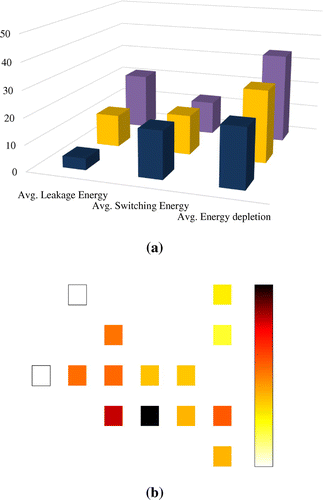
To estimate the energy depletion of outlined circuit, we used QCAPro (Srivastava, Asthana, Bhanja, & Sarkar, Citation2011). The consumption is determined in several tunneling energy stages at 2 K temperature, presented in Table . Moreover, the average switching energy, average leakage energy and average energy depletion at three different tunneling energy stages of outlined circuit are shown in Figure .
Table 2. Energy depletion study of proposed RS Flip-flop
Figure 9. (a) Average leakage energy, switching energy and total energy depletion at three distinctive tunneling energy (T = 2.0 K) levels and (b) Energy depletion map for the outlined QCA circuit at 2 K temperature with 1.5 Ek.
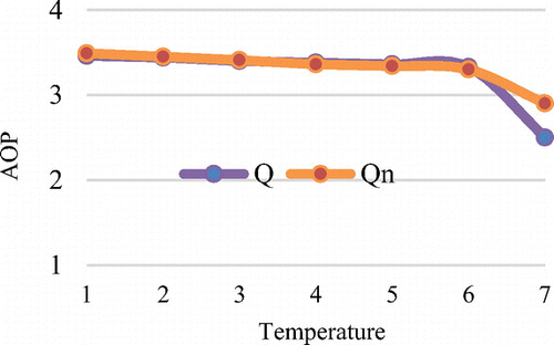
4.3. Consistency of the proposed circuit
The average output polarization (AOP) of the circuit is lessened by rising the temperature (Hassan et al., Citation2017). The temperature consequence on the AOP of the outlined circuit is shown in Figure . The AOP of the RS flip flop is steadily lessened, up to a temperature of T = 6 K. Hence, in between 1 and 6 K, the proposed circuit functions competently. Beyond that temperature the AOP is depleted, and the circuit breakdowns. To assemble the AOP at several temperatures, the circuit is simulated with QCADesigner and the highest and lowest polarizations for every output are studied. For instance, at T = 1 K, the highest and lowest polarizations of output cell of flip-flop are 9.42 and –9.42e−1, respectively. Therefore, the AOP for output cell Q is [(9.42e−1)–(–9.42e−1)]/2 = 3.46. Similarly, others AOPs for different cells of each layout at separate temperatures are estimated and presented in Figure .
Figure 10. Impact of temperature on AOP of RS flip-flop.
5. Conclusion
This paper, an advanced and uncomplicated QCA layout of RS flip-flop is analyzed. The outlined circuit is confirmed with the QCADesigner and QCAPro tool. In contrast with the earlier study, the outcomes presented that proposed flip-flop is improved in terms of dimension, cell number, and delay. Moreover, the layout does not involve any rotated cells and it is efficient in terms of energy and reliability where the design have been permitted with QCADesigner. The proposed design present superior possibilities to significantly inflate the performance precisely for conceiving higher power-competent excessive efficiency circuit structures. Thus, this structure can be utilized to design circuits for nanocomputing and applying such competent circuit will absolutely be a revolution in the field of computation.
Funding
The authors received no direct funding for this research.
Acknowledgments
The authors would like to thank the anonymous reviewers who have contributed to this work. As well Mr Kawser Ahmed for reviewing the draft and providing inputs to alternative QCA views.
Additional information
Notes on contributors
Md. Abdullah-Al-Shafi
Md. Abdullah-Al-Shafi received his B.Sc (Engg.) in 2015. Currently pursuing an MS in Information Technology (IT) in Institute of Information Technology (IIT), University of Dhaka, Bangladesh. He has 19 research publications in renowned international journals and conference. His research area includes Distributed Computing, Quantum-dot Cellular Automation, Intelligent System and Wireless Sensor Network.
Related Research Data
References
- Abdullah-Al-Shafi, M. (2016a). Analysis of fredkin logic circuit in nanotechnology: An efficient approach. International Journal of Hybrid Information Technology, 9(2), 371–380.10.14257/ijhit
- Abdullah-Al-Shafi, M. (2016b). Synthesis of Peres and R Logic circuits in nanoscopic scale. Communications on Applied Electronics, 4(1), 20–25.10.5120/cae2016652004
- Abdullah-Al-Shafi, M., Aneek, R. H., & Bahar, A. N. (2017). Universal reversible gate in quantum dot cellular automata (QCA): A multilayer design paradigm. International Journal of Grid and Distributed Computing, 10(1), 43–50.10.14257/ijgdc
- Abdullah-Al-Shafi, M., & Bahar, A. N. (2016a). Novel binary to gray code converters in QCA with power dissipation analysis. International Journal of Multimedia and Ubiquitous Engineering, 11(8), 379–396.10.14257/ijmue
- Abdullah-Al-Shafi, M., & Bahar, A. N. (2016b). Optimized design and performance analysis of novel comparator and full adder in nanoscale. Cogent Engineering, 3(1), 1237864.
- Abdullah-Al-Shafi, M., & Bahar, A. N. (2016c). QCA: An effective approach to implement logic circuit in nanoscale. Presented at the 5th International Conference on Informatics, Electronics & Vision (ICIEV), International Conference on, IEEE, Dhaka, Bangladesh, 620–624.
- Abdullah-Al-Shafi, M., & Bahar, A. N. (2017). A novel binary to grey and grey to binary code converter in majority voter-based QCA nanocomputing. Journal of Computational and Theoretical Nanoscience, 14, 2416–2421.10.1166/jctn.2017.6842
- Abdullah-Al-Shafi, M., Bahar, A. N., Ahmad, F., & Ahmed, K. (2017). Performance evaluation of efficient combinational logic design using nanomaterial electronics. Cogent Engineering, 4(1), 1349539.
- Abdullah-Al-Shafi, M., Bahar, A. N., Ahmad, F., Bhuiyan, M. M. R., & Ahmed, K. (2017). Power analysis dataset for QCA based multiplexer circuits. Data in Brief, Elsevier, 11, 593–596.10.1016/j.dib.2017.03.001
- Abdullah-Al-Shafi, M., Bahar, A. N., Habib, M. A., Bhuiyan, M. M. R., Ahmad, F., Ahmad, P. Z., & Ahmed, K. (in press). Designing single layer counter in quantum-dot cellular automata with energy dissipation analysis. Ain Shams Engineering Journal. doi: 10.1016/j.asej.2017.05.010
- Al Shafi, A., Bahar, A. N., & Islam, M. S. (2015). A quantitative approach of reversible logic gates in QCA. Journal of Communications Technology, Electronics and Computer Science, 3, 22–26.10.22385/jctecs.v3i0.33
- Bahar, A. N., Uddin, M. S., Abdullah-Al-Shafi, M., Bhuiyan, M. M. R., & Ahmed, K. (2017). Designing efficient QCA even parity generator circuits with power dissipation analysis. Alexandria Engineering Journal, Elsevier. ( In press). doi:10.1016/j.aej.2017.02.002
- Biswas, P. K., Bahar, A. N., Habib, M. A., & Abdullah-Al-Shafi, M. (2017). Efficient design of Feynman and Toffoli gate in quantum dot cellular automata (QCA) with energy dissipation analysis. Nanoscience and Nanotechnology, 7(2), 27–33. doi:10.5923/j.nn.20170702.01
- Choi, M. (2005). A study on a Quantum-dot Cellular Automata based asynchronous circuit design. M.S., Oklahoma State University, 49, 1431653.
- Cowburn, R. P., & Welland, M. E. (2000). Room temperature magnetic quantum cellular automata. Science, 287(5457), 1466–1468.10.1126/science.287.5457.1466
- Dutta, P., & Mukhopadhyay, D. (2014). New architecture for flip flops using quantum-dot cellular automata. In ICT and Critical Infrastructure: Proceedings of the 48th Annual Convention of Computer Society of India-Vol II (pp. 707–714). Cham: Springer. doi: 10.1007/978-3-319-03095-1_77
- Hassan, M. K., Nahid, N. M., Bahar, A. N., Bhuiyan, M. M. R., Abdullah-Al-Shafi, M., & Ahmed, K. (2017). Dataset demonstrating the temperature effect on average output polarization for QCA based reversible logic gates. Data in Brief, Elsevier, 13, 713–716.10.1016/j.dib.2017.06.058
- Hennessy, K., & Lent, C. S. (2001). Clocking of molecular quantum-dot cellular automata. Journal of Vacuum Science and Technology, 19(5), 1752–1755.10.1116/1.1394729
- Huang, J., Momenzadeh, M., & Lombardi, F. (2007). Design of sequential circuits by quantum-dot cellular automata. Microelectronic Journal, 38(4), 525–537.10.1016/j.mejo.2007.03.013
- Islam, S., Shafi, M. A., & Bahar, A. N. (2015). Implementation of binary to gray code converters in quantum dot cellular automata. Journal of Today’s Ideas – Tomorrow’s Technologies, 3(2), 145–160.10.15415/jotitt.2015
- Islam, M. S., Shafi, M. A., & Bahar, A. N. (2016). A new approach of presenting universal reversible gate in nanoscale. International Journal of Computer Applications, 134(7), 1–4.10.5120/ijca2016910208
- Jagarlamudi, H. S., Saha, M., & Jagarlamudi, P. K. (2011). Quantum dot cellular automata based effective design of combinational and sequential logical structures. World Academy of Science, Engineering and Technology, 60, 671–675.
- Landauer, R. (1961). Irreversibility and heat generation in the computing process. IBM Journal of Research and Development, 5(3), 183–191.10.1147/rd.53.0183
- Lent, C. S., Tougaw, P. D., Porod, W., & Bernstein, G. H. (1993). Quantum cellular automata. Nanotechnology, 4(1), 49.10.1088/0957-4484/4/1/004
- Liu, W., Lu, L., O’Neill, M., & Swartzlander, E. E. (2014). A first step toward cost functions for quantum-dot cellular automata designs. IEEE Transactions on Nanotechnology, 13(3), 476–487.
- Mitic, M., Cassidy, M. C., Petersson, K. D., Starrett, R. P., Gauja, E., Brenner, R., & Jamieson, D. N. (2006). Demonstration of a silicon-based quantum cellular automata cell. Applied Physics Letters, 89(1), 13503.10.1063/1.2219128
- Orlov, A. O., Amlani, I., Bernstein, G. H., Lent, C. S., & Snider, G. L. (1997). Realization of a functional cell for quantum-dot cellular automata. Science, 277(5328), 928–930.10.1126/science.277.5328.928
- Rezaei, A. (2017). Design of optimized quantum-dot cellular automata RS flip flops. International Journal of Nanoscience and Nanotechnology, 13(1), 53–58.
- Roohi, A., Khademolhosseini, H., Sayedsalehi, S., & Navi, K. (2014). A symmetric quantum-dot cellular automata design for 5-input majority gate. Journal of Computational Electronics, 13(3), 701–708.10.1007/s10825-014-0589-5
- Sen, B., Dutta, M., Some, S., & Sikdar, B. K. (2014). Realizing reversible computing in QCA framework resulting in efficient design of testable ALU. ACM Journal on Emerging Technologies in Computing Systems, 11(3), 30:8–30:22.
- Shafi, M. A., Islam, M. S., & Bahar, A. N. (2015). A review on reversible logic gates and it’s QCA implementation. International Journal of Computer Applications, 128(2), 27–34.10.5120/ijca2015906434
- Shin, S.-H., Jeon, J.-C., & Yoo, K.-Y. (2013). Wire-crossing technique on quantum-dot cellular automata. In Proceedings – 2nd International Conference on Next Generation Computer and Information Technology, 52–57.
- Smith, C., Gardelis, S., Rushforth, A., Crook, R., Cooper, J., Ritchie, D., … Pepper, M. (2003). Realization of quantum-dot cellular automata using semiconductor quantum dots. Superlattices and Microstructures, 34(3), 195–203.10.1016/j.spmi.2004.03.009
- Srivastava, S., Asthana, A., Bhanja, S., & Sarkar, S. (2011). QCAPro-an error-power estimation tool for QCA circuit design. In 2011 IEEE International Symposium of Circuits and Systems (ISCAS), 2377–2380.
- Tougaw, P. D., & Lent, C. S. (1994). Logical devices implemented using quantum cellular automata. Journal of Applied Physics, 75(3), 1818–1825.10.1063/1.356375
- Tougaw, P. D., & Lent, C. S. (1996). Dynamic behavior of quantum cellular automata. Journal of Applied Physics, 80(8), 4722–4736.10.1063/1.363455
- Vetteth, A., Walus, K., Dimitrov, V. S., & Jullien, G. A. (2003). Quantum-dot cellular automata of flip-flops. The National Conference on Communications (NCC), 368–372.
- Walus, K., Dysart, T. J., Jullien, G. A., & Budiman, R. A. (2004). QCADesigner: A rapid design and simulation tool for quantum-dot cellular automata. IEEE Transactions on Nanotechnology, 3(1), 26–31.10.1109/TNANO.2003.820815
- Walus, K., & Jullien, G. A. (2006). Design tools for an emerging SoC technology: Quantum-dot cellular automata. Proceedings of the IEEE, 94(6), 1225–1244.10.1109/JPROC.2006.875791
- Wang, Y., & Lieberman, M. (2004). Thermodynamic behavior of molecular-scale quantum-dot cellular automata (QCA) wires and logic devices. IEEE Transactions on Nanotechnology, 3(3), 368–376.10.1109/TNANO.2004.828576