
Abstract
The current work is to conduct a design review on a multipurpose power socket for home application with the latest state of art features. Reviews are done in the areas of standard and codings, material selections, universal adapters, sensors and lighting technology. The standards for fabrication of BS 546 and BS 1363 plugs and sockets are essential for safety purposes. Together with selection of suitable material in production of plug and sockets, the occurrence of accidents can be averted. The invention of universal adapters was first coined by Rumble in year 1982 marks an evolution in the history of plugs and sockets. The main focus was to cater the different plug fixtures in various countries. Coupled to this, review works on the various types of sensors and lighting technologies is provided since it could be fused to the universal plug adapters for various applications. This paper then go on in proposing future works which could open new research pathways among worldwide researchers.
PUBLIC INTEREST STATEMENT
Novel home power socket applications are becoming consumers’ choices in selecting an energy efficient product. In recent years, power sockets have been invented in such a way where additional functions and features have been added to it. This article illustrates the standards and coding’s and material selections in fabricating power sockets. Besides, the evolutions of universal adapters, sensors and lighting technologies are also reviewed in this article. The idea of SnapPower© socket technology is discussed here too. The “plug and play” mechanism from the universal adapter can be applied in producing a brand new socket type. By incorporating both light emitting diode and sensors, the socket itself can be further developed into a smart socket which features a sensor lighting system. By conducting further research and studies, the multipurpose power socket may undergoes further evolution and modification which will impact our life.
1. Introduction
Light is an important element in human’s daily activities as it provides brightness in the dark. There are varieties of light source that are being adopted in today daily life such as fire, halogen lamp, fluorescent lamp and light emitting diode (LED) lamp. LED has been chosen as one of the most common lighting systems due to the advantage in energy saving, better luminous and it can be used for a longer period of time. Sensors is also focused in current lighting technology. Sensors will act as a switch and only be functioned as it detects the gesture related to its specification such as motion or darkness. The usage of sensor in lighting system will further improve the efficiency of the system and provides an alternatives for energy saving. Figure shows the research interest on passive infrared ray (PIR) sensor in 2007–2016. Figure illustrates the research interest on LED bulbs from year 2007 to 2016.
Figure 1. Research works on PIR sensor from 2007 to 2016.
Source: https://scholar.google.com/scholar?q=PIR+sensor&hl=en&as. Keyword used: PIR sensor.
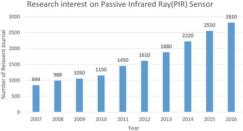
Figure 2. Research works on LED bulb from 2007 to 2016.
Source: https://scholar.google.com/scholar?hl=en&as_sdt=0,5&q=light+emitting+diode+bulb. Keyword used: Light Emitting Diode Bulb
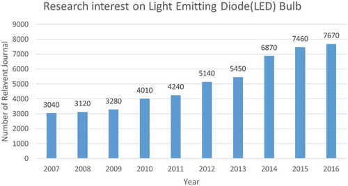
Both Figures and demonstrate a gradual increment in the number of research done. This shows that the market interest in PIR sensors and LED lights are increasing with the number of years. Therefore, based on the statistics from Figures and , the authors decided to dedicate a review work on different types of electrical power sockets coupled with state of the art design which incorporate different types of lighting and sensors technology for home applications. The review works will start with a brief overview on the standards and codings implemented, followed by the types of material used on the development of universal adapters and their applications. On the other hand, different types of sensors and lighting technology will be discussed in this work. Last but not least, proposed future works will be presented which could help to open new research pathways in the future.
2. Standards and coding’s
Standards are the regulations developed by International Standards Organizations (ISO). These standards act as the benchmark to be referred and used worldwide. Standards are documented to overcome differences among standards and technical regulations developed independently and separately by each nation or national standard organization. Codings is a set of rules that specify the standards that need to be followed to fabricate an object mentioned under the standard and codings.
Plugs and wall sockets are the electrical components that connect together to allow the flow of electricity and thus complete the circuit. Plug and sockets are invented in Britain in the beginning of 1880s and designed to have only 2 pins at that time. The official standards then come in when the idea of interchangeable compatible devices were proposed. BS 1363 is the British standards that is used in United Kingdom and mostly the Commonwealth countries. It is a type of single-phase AC power plugs and sockets that can support a voltage up to 250V and a variety of ampere such as 2A, 5A, 13A and 15A.
By referring to 13 A plugs, socket-outlets, adaptors and connection units, there are standards that need to be follow strictly in order to produce a marketable wall sockets with inspection on safety purposes. The sockets shall have marking the necessary information on the parts where it can be read and will not be easily spoiled. This includes:
name, trademark of the responsible vendor,
the codes of British Standards, BS 1363,
on rewirable adaptors, the terminals for connection of the various conductors shall be identified by symbols (I. British Standard, Citation1995),
the word “FUSE” or “FUSED” or the symbol need to be marked on the surface of the adaptor for fused adaptors (I. British Standard, Citation1995)
adaptors other than shavers shall marked with the maximum allowable amperes for electrical load, such as “MAX 13 A” (I. British Standard, Citation1995),
adaptors shall be marked with the allowable voltage and nature of supply for suitable electrical loads (I. British Standard, Citation1995),
the colour codes for wire to connects needs to be marked referring to the matching below (I. British Standard, Citation1995),
Green/Yellow Earth (if any)
Blue Neutral
Brown Live
Table illustrates common types of symbol marked on adaptors.
Table 1. Symbol marked on adaptors
There are specific safety requirements to be followed for BS 1363 wall adaptor. These can be divided according to 3 types of sockets which are 5A 3-round-pin adaptor, 12A 3-rectangulat-pin adaptor and 15A 3-round-pin adaptor.
5A 3-round-pin adaptors are referred to BS 546 as international standard. To design and manufacture BS 546, it must have protection from fuse-link conforming to BS 1362 together. Only an allowable current of not exceeding 5A is permitted for the operation of this adaptor. A 5A adaptor with not more than three 5A sockets protected by one 5A main fuse-link confirming to BS 646 or BS 1362 is permitted (International Organization for Standardization [ISO], Citation2007).
For 12A 3-rectangular-pin adaptor, the fabricating and designing process should be based on the BS 1363 Part 3 standard. The 13A adaptor that has one or two sockets for 13A plugs conforming to BS 1363 Part 1 need not be fused. For multiway 13A adaptor that has more than two sockets for 13A plug conforming to BS 1363 Part 1, it should have a 13A fuse-link conforming to BS 1363 as protection. For multiway 13A adaptor that has one socket for 12A plug and another socket for 5A plug conforming to both BS 1363 Part 1 and BS 546, respectively, an appropriate fuse-link complying with BS 546 and BS 1362 should be used to protect the outgoing circuits through 5A sockets (ISO, Citation2007).
While 15A 3-round-pin adaptor is manufactured and designed to BS 546 standard. A 15A adaptor is protected by fuse-link matching to BS 1362. Table shows the number ratings and the current ratings of the socket configuration of 15A adaptor (ISO, Citation2007).
Table 2. Number and current rating of sockets
The safety features of BS 1363 adaptor or wall socket is further enhanced with the usage of safety shutters. The safety shutters is used as such that when a plug is withdrawn from it, the sockets contacts or the socket holes which carry current supply will be automatically closed. The shutters should be operated by mating the earth pin to the earth hole. The shutter for a particular socket aperture should not be able to closed the shutter for another socket aperture independently (ISO, Citation2007).
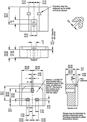
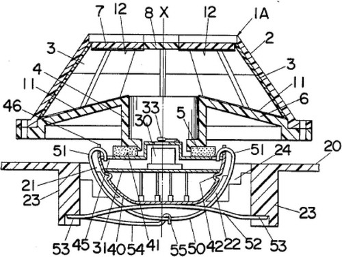
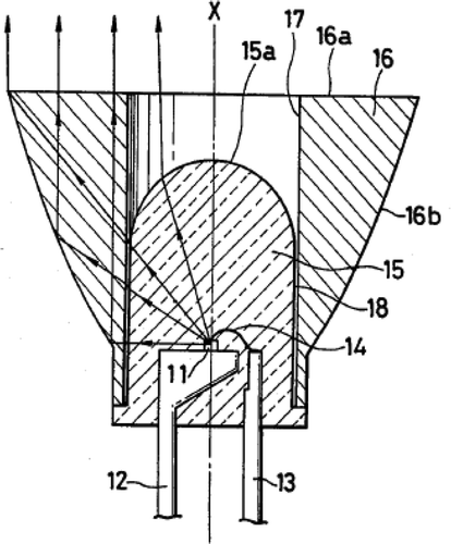
Figure illustrates the standard dimension used in fabricating a BS 1362 type wall socket (Saudi Standards, Metrology and Quality Org [SASO], Citation2010). The dimension of the sockets must be strictly followed to ensure that the plug will fit firmly to the socket when using it to avoid accidents to be happened.
Figure 3. The dimension of wall sockets BS 1362.
In Malaysia, the fabrication and manufacturing of wall sockets must follow the information booklet of Approval of Electrical Equipment (Electricity Regulation 1994).This regulation is established by Energy Commission Malaysia under the Energy Commission Act 2001 [Act 610]. Under this regulation, a socket outlet is described as an electrical device that is fixed at a point at which wiring terminates. It provides a detachable connection with the pins of a plug and it has two or three contacts with a maximum current rating of 15A. Table shows the standard codes of wall socket used in Malaysia.
Table 3. Wall socket standards codes used in Malaysia (Energy Commission Malaysia, Citation2009)
The abbreviation of MS in Table refers to Malaysia Standard, IEC refers to International Electrotechnical Commission and BS refers to British Standard. By ensuing the procedure of these standards, the respective vendor can apply for certification of approval for electrical equipment with SIRIM Berhard. Upon obtaining the certifications, the vendors’ product is labelled as approved regulated electrical equipment and can be sold in Malaysia’s market.
3. Material selection
Material selection is important in the fabrication works of a power socket. This is to ensure that the socket produced is durable and safe for its user. The main components of power socket are made up of plastics and brass. Plastics are used as the casing and inner structure for the socket. Brass is used as connectors to hold the plug pin to allow the flow of electricity to the electrical appliances.
Plastics can be divided into two type of categories which are synthetic or semi-synthetic organic compounds and this type of plastics are mostly derived from petrochemical. It is made by building up from simple chemical substances. To ensure the plastics bonding are tougher, safer, and cleaner, polymers that build up plastics are added with complex blend of materials known as “additives” (Talbot, Citation1941). These include biodegradable plasticisers, flame retardants, and heat stabilizers. The grade of plastics used in socket manufacturing is mainly thermoplastics or thermosetting polymers. Thermoplastics are plastics that will not undergo physical or chemical change in their composition upon heated (Gilleo, Citation2004). Thermosetting polymers, on the other hand can melt and take shape only once. They remains in solid once they have solidified. There are few common plastics grade that are used in fabricating power socket.
Phenolic is one of the plastics used in manufacturing process. It act as a good electrical insulators and able to withstand resistance against water, acid and most solvents. It has low thermal conductivity and rigid at room temperature. The normal operating temperature limit for phenolic molding is 150°C, but grades are available which will operate at up to 200°C for limited periods. These properties allow it to be used in electric appliances industry (Black, Citation2010). There are two main production methods. One reacts phenol and formaldehyde directly to produce a thermosetting network polymer, while the other restricts the formaldehyde to produce a prepolymer known as novolac which can be molded and then cured with the addition of more formaldehyde and heat (Gardziella, Pilato, & Knop, Citation2000; Hesse, Citation2004).
Melamine formaldehyde, or melamine is another type of plastics that is used due to its strong and glossy properties. Melamine shows good resistance to heat, chemicals, moisture, electricity and scratching which makes it to have excellent molding properties in producing power sockets and plugs (Black, Citation2010). Melamine formaldehyde was discovered by William F. Talbot and patent was applied on 12 December 1936 (Talbot, Citation1941).
Another type of plastics that is widely used is polyimide. Thermosetting polyimide is one of the highest performing engineering plastics, with superior performance in applications under severe conditions. The properties of polyimide materials include:
high temperature resistance that have operating temperature of 315°C,
high wear resistance,
low thermal expansion,
good thermal and electrical insulation,
relatively easy to machine,
With this properties, thermosetting polyimides are used in various types of manufacturing industries including automotive, electrical appliances, aircraft and aerospace (Black, Citation2010). These materials tend to be insoluble and have high softening temperatures, arising from charge-transfer interactions between the planar subunits (Liaw et al., Citation2012).
Brass is the material used as the electrical conductor inside the wall socket. Brass is a material that is made of copper and zinc. Copper-zinc solid solution alloy or brass retains good corrosion resistance and formability of copper but are relatively stronger (Fungal & Brody, Citation1996). Brass is used widely in the socket manufacturing due to its properties and it is a cheaper material compare to gold. Brass is generally soft which means that it can be machined without the use of cutting fluid, though there are exceptions to this (Faraday, Citation1832). Brass is used in situations where it is important that sparks are not struck, for example use as a fittings and tools that near flammable or explosive materials. CL 15000 99.85Cu-0.15Zr or zirconium-copper is one of the brass used in fabrication process. It has elastic modulus of 129 GPa and fatigue strength of 180 MPa. The density of CL 15000 is 8.89 g/cm3 and it has a liquidus temperature of 1080°C. The electrical conductivity of 93% IACS at 20°C. CL 15000 can withstand a temperature up to 1080°C before it melts 93% IACS shows that it is a good electrical conductor. Another similar brass or copper alloy, CL 15100 shows a similar properties as in CL 15000. This alloy is called ZHC copper and the elastic modulus is slightly smaller (121 GPa), the density is larger (8.94 g/cm3) and the liquidus temperature is the same at 1080°C. However, CL 15100 is a better conductor of electricity with 95% IACS if it is annealed and 90% if it is rolled with volumetric at 20°C (Fungal & Brody, Citation1996).
The material used for doing the conductors inside wall socket but be able to withstand overheating. If the holders are getting hotter relative to time, there will be a risk of fire. The heating comes from the current which is drawn by the appliance and the resistance of the conductor. The plug pin will be inserted to or removed from the socket when using it. If the material wears too much, the holder may not be able to hold the plug pins firmly. Besides, the material used must be in low cost to keep the material and processing costs down.
The material used to fabricate an electrical wall socket is crucial in safety purposes. Failure of the material used may possess danger like electrical sparking. Types of plastics used must be a good electrical insulator to avoid the electricity to be channelled into area other than the socket holes that fit in electrical plug. Types of brass used must have good ductility to ensure that the holder of the socket will always mate with the plug pin tightly and allow electricity to flows through efficiently.
By selecting the right material in fabrication, problems like electrical sparking can be avoided. Electric sparking is an abrupt electrical discharge that occurs when a sufficiently high electric field creates an ionized, electrically conductive channel through a normally insulating medium, often air or other gases or gas mixtures. Faraday described this phenomenon as “beautiful flash of light attending the discharge of common electricity (Faraday, Citation1832). By rapid transitioning of electric field from a non-conducting to a conductive stats, it will produce a brief emission of light and a sharp crack or snapping sound.
Fire is one of the major disasters around the world and electrical fire is the leading type of fire in terms of occurrence rate. An analysis is done in China and the leading type of fault resulting in major electrical fires is short circuit (43.89%) while the second leading fault is loose contact accounting for 8.89%. The second type of faulty is more difficult to discover as it is always covered by some illusions including short circuits. A study to such fires also known as sparking was conducted by Zi-Bo, Man, Chang-Zheng, and Ming (Citation2011). First, two different types of loose contact fault, contact area reduction and contact vibrations are simulated tested and the temperature and some electrical parameters of contact resistance are tabulated during the testing. With this results, the characteristic identification criterion for loose contact is proposed (Zi-Bo et al., Citation2011).
In the experiment, plugs and sockets of rated current 10A are used under conditions of reduction and contact areas and contact vibrations. External heating temperature of 100°C, 200°C, 300°C, 400°C, 500°C, 600°C and 700°C are used to determine the characteristic law of samples. Apparently the plastics insulations of shells are melted and deformed while the metal parts are carbonized but there is no sign of melting and deformation. From the analysis results, it can be concluded that under fault over a small contact area, the plug’s terminal could reach a temperature of 300–400°C and the contact area between plug and socket can reach a temperature of 200–300°C. The major problem in sparking is after melting and carbonizing of insulation material of wall socket, secondary fault including combustion and short circuit may happen directly (Techakittiroj, Citation2008).
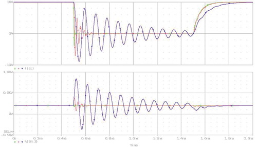
The inductance of the wall sockets will result in creating sparks. When the outlet is unplugged, the inductance in the distributed system resists the change in the current. The path for the current has to be created and it is only active when the socket is unplugged. The rising voltage appears mainly at the outlet terminal and the major concern is to reduce the voltage at the socket. By reducing the voltage, the electrical sparks on the contact surface can be eliminated and this improves the socket lifetime. A capacitor is used to absorb energy from the inductance where the voltage will be regulated by the capacitor. By combining a capacitor with an inductor will result an oscillation at the voltage terminal and prolongs the durations of high voltage at the terminal. A resistor is used to damp the oscillation (Techakittiroj, Citation2008). Figure shows the PSpice circuit for analysing a socket outlet.
Figure 4. PSpice circuit for analysing a socket outlet.
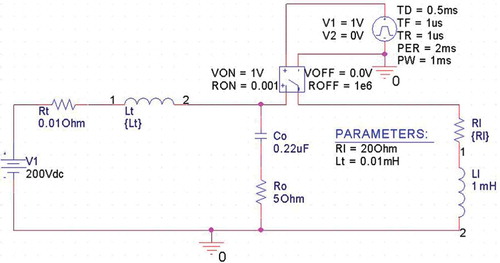
The simulations is done by adding a capacitor of 0.22 μF and a resistor of 5Ώ to the outlet side. The simulations runs on three different value of inductance: 0.01mH, 0.1mH and 1mH (Techakittiroj, Citation2008). Figure illustrates simulation results by adding inductance into the socket outlet circuit.
Figure 5. Simulation result when the inductance is added into socket outlet circuit.
Blue line indicates the variation of inductance; Red line indicates the resistance; Green line indicates the capacitance
The effect of load on the protection circuit is simulated. The power consumption varies on different values, from a very small amount such as mobile phone charger to a very large amount such s air-conditioner. The loads used in simulation are 8Ώ (25A), 20Ώ (10A), 200Ώ (1A) and 2k Ώ (0.1A) (Techakittiroj, Citation2008). Figure shows the simulation result by adding resistance into the circuit.
Figure 6. Simulation result when the resistance is added into socket outlet circuit.
Green line indicates inductance; Red line indicates capacitance; Blue line indicates the power supply; Yellow line indicates the added resistance
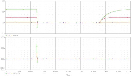
From the simulation result it can be seen that larger load will produce larger maximum overshoot. The resistance and capacitance value is increasing as to reduce the maximum overshoot. By adding resistor and capacitor to the circuit on the wall socket, the probability of electric sparks to occur can be minimized.
4. Universal adapters
The applications of universal adapters will aid in designing the multipurpose power socket. Universal adapter was first invented by Clive S. Rumble in 1982 and patented in 1985. He picked up the idea of inventing such adapter as it was convenience for a user to use his or her particular plug pin in another foreign country. Universal adapter is a type of adapter used mostly during travelling as not all country are using the same type of plug and socket as in BS 1362 or Type G standard. The universal adapter has built in transformer and rectifier to step down the voltage supply to 120V and to change the AC voltage into DC voltage to meet the country’s voltage and current supply.
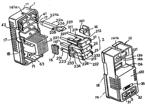
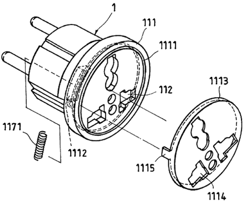
A universal adapter with patent no. US 5159545 was invented by Lee. This adaptor has different types and shape of plug pins located at one end of the adapter. These plug pins is matched with different types of wall socket across the world. The adaptor has a convertor which consists of a transformer and a rectifier for transforming or rectifying an input power. The socket for the plug pins to fit in is located on the other side of the adaptor which is made to be a universal sockets for different types of plug. The selected plug pins of the adaptor is pushed out from the other side and a slidable locking members used to lock the plug pin used. When the adapter is not used, the locking members is pulled to the opposite direction and the pins can be pushed back into the adaptor (Lee, Citation1992). Figure shows the exploded view of universal adapter US 5159545.
Figure 7. The universal adapter of patent no. US 5159545.
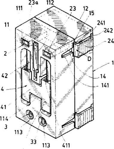
Another universal adapter patent no. US 5791921 was invented by Lee. The working mechanism is similar to the previous adaptor but there are some differences. The plug pins are located at one side while the sockets are located in the other side. The rectangular pins and the flat blades pins are located at both ends of the adaptor. It can be extended or retracted using the seesaw buttons located at the sides of it. When extending the rectangular pins, the ground pin will be simultaneously biased for its forward extending to form triple rectangular shaped pins (Lee, Citation1998). The third pins consists of a pair of round pins and it can be horizontally extended when in used. Figure illustrates the isometric view of universal adapter US 5791921.
Figure 8. The universal adapter of patent no. US 5791921.
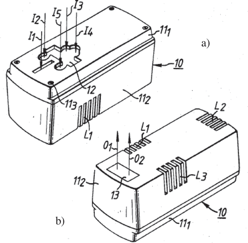
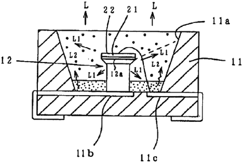
In the third universal adapter patent no. US 4543624, the working principle is similar to the previous 2 adapter on how the plug pins is pulled out and pushed back. However, this adapter features a louvres on the position of L1, L2 and L3 to allow any heat generated therein to be readily dissipated (Rumble, Citation1985). Figure illustrates the isometric view of this universal adapter where Figure (a) shows the bottom view of the adapter while Figure ) shows the top view of the adapter.
Figure 9. The universal adaptor of patent no. US 4543624.
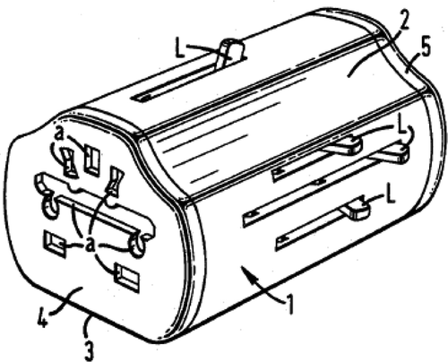
An adapter Patent No. US 4626052 was invented by Rumble. It features a universal adapter which is wider instead of taller in the previous 3 design. The whole adapter is in a cylindrical shape. The adapter contains a stack of sliding pin carriers. The pin array can be extended or retracted by operating lugs L protruding from the side of the casing. Releasable detents associated with the lugs locate the sliding carriers in the forward and retracted conditions.(Rumble, Citation1986) Figure shows the isometric view of the respective universal adapter.
Figure 10. The universal adaptor patent no. US 4626052.
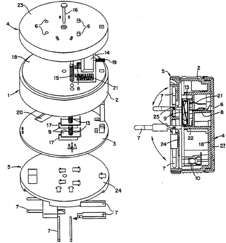
The fifth universal adapter patent no. US 5474464 was invented by Drewnicki. This device comprises of a carrier member that is mounted on the housing. There are also different types of selectable pin arrays disposed on the carrier member which can be operated one at a time by rotation of the carrier relative to the housing. A plurality of socket arrays are also rotatable are mounted on the aperture member on the other side of the housing. By rotating the members of the housing, the socket arrays is selected and it can be operated only one at a time too. The plug pins of the selected pin arrays are pivotally mounted on the carrier member so that they can be extended outwardly to be connected to wall socket and moved to a retracted inoperative position when not in use (Drewnicki, Citation1995). Figure illustrates the exploded view of the patented universal adapter.
Figure 11. The universal adapter of patent no. US 5474464.
In the next 3 universal adapter inventions, the working mechanisms are similar that are changing the plug pins of the adaptor to a suitable type when using it. In Wong’s invention patent no. US 6942508, there is a bayonet fitting at the base. The bayonet fitting of the base is created to secure the body to the base in a desire orientations. There are electrical contacts configure on the body to engage with the terminals of the base when the body and base are secured to one another(Wong, Citation2005). The pins piece is rotated to body in clockwise direction to lock it and vice versa to remove it. Figure shows the isometric view of the bayonet fittings of adapter US 6942508. While in an invention of Philips, Fischer, and Fyke (Citation2013) patent no. US 6845023, there are different types of adaptor plug configured to mate with the socket. The adapter has a locking mechanism operative to lock the adaptor plug into the socket. A detent button is located on the sides of the adapter and it is pressed to either lock or release the adaptor plug to or from the socket (Philips et al., Citation2013). Figure shows isometric view of this patented adapter. In an invention of Lee and Li (Citation2001) (patent no. US 6328591), the pins can be switched according to the type of sockets used. The face panel may be equipped with a safety cover. The peripheral mounting stripes are attached to the periphery of face panel, the inwardly extended hooked portion of each mounting strip is hooked on the back side wall of the face panel to let the safety cover be rotated on the face panel. When in use, the safety cover is rotated on the face panel to move the insertion holes into alignment with the plugholes for installation of any variety of electric plugs (Lee & Li, Citation2001). Figure shows the isometric view of this invention.
Figure 12. The bayonet fitting of adapter patent no. US 6942508.
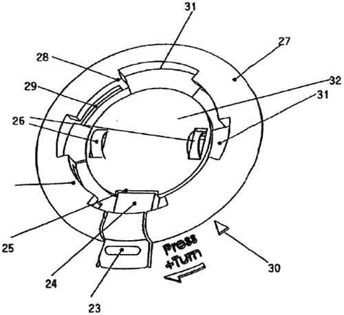
Figure 13. The universal adapter patent no. US 6845023.
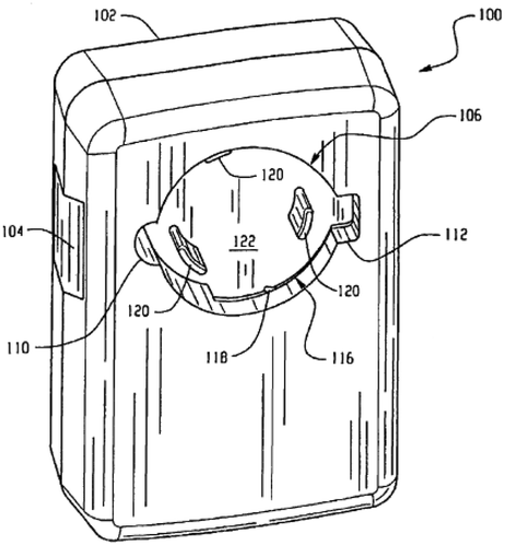
Figure 14. The universal of adapter patent no. US 6328591.
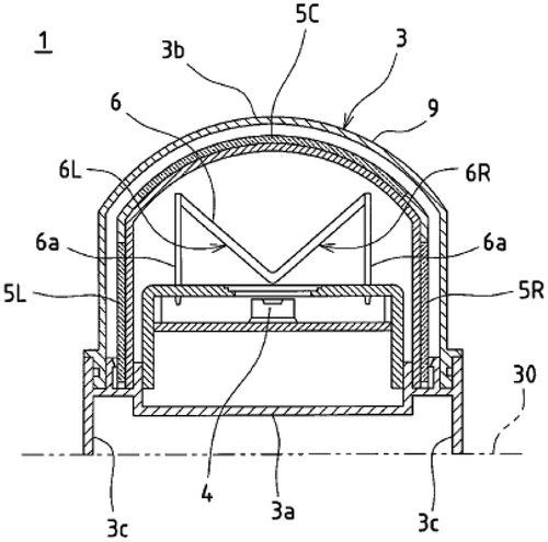
There is no product available in the market today regarding the multipurpose power socket. However, there is a similar product which combining a socket with the sensor lighting system,SnapPower© Guidelight. SnapPower© launched The SnapPower© Guidelight in March 2014. It is a replacement for the standard electrical outlet cover at home. The guide light will have LED lighting system on the lower part to provide illumination at night. The LED lighting system will be automatically switched on or off with the aid of a build in light sensor.
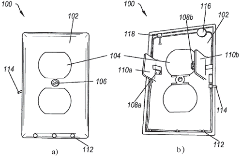
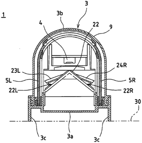
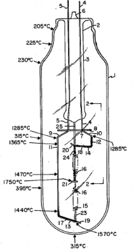
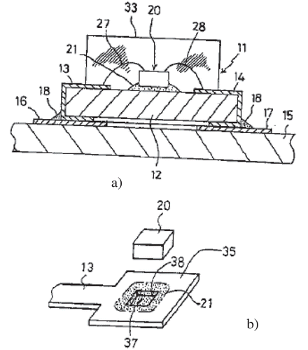
An invention was proposed by Smith (Patent No. US 8912442) in 2014. The cover plate includes electrical receptacle and two conductor strips. The first conductor strip on the left and the other conductor strip on the right. The conductor strips are located at the middle rearward direction of the plate. When the plate is snug into the socket, the first conductor strip is contacted to the electrical receptacle that is connected to a power source. Similar procedure will done on the second conductor strip is snug into the socket. The cover plate also includes an insulating material to prevent both conducting strip from contacting with other conducting materials. The lower front part of the cover plate has a photocell that can detects photons either in visible range or infrared range. The photocell acts as a switch to turn the LED bulb at the lower base of the cover plate on or off (Smith, Citation2014). Figure (a) illustrates the front view of the patented active cover plate and Figure (b) illustrates the back view of the patented active cover plate.
Figure 15. Design of active cover plate US 8912442.
The improvement of the active cover plate was done by Smith et al. (Citation2015). In this invention, the conductor strips are replaced with spring clip. The spring clip is adjustable in both horizontal direction and vertical direction with respect to the faceplate to reach screw terminals with different depth. The spring clip has an electrical conductive portion that is connected to the faceplate and a non-conductive portion connected to the opposite end of the conductive portion. The active cover plate is designed to have adjustability in order to connect to a wide range of outlet bodies. It can be adjusted in X direction to accommodate different heights, in Y direction to accommodate screw terminals that have different depth and in Z direction to accommodate different width. The lower side of the cover plate has an externally accessible power supply for universal serial bus (USB) charger or other circuitry. There are two USB ports to allow the user to charge two devices at the same time. The lower part of the cover plate can be also accommodated with guidelight mechanism. This mechanism includes a light sensor aperture on the front face and few light emission apertures on the bottom. The light emission aperture id available in different shape and size to fulfil the desire product look (Smith et al., Citation2015). Figure illustrates back view of the active cover plate with (a) the spring clip in elevated position; (b) the spring clip in its original position.
Figure 16. Spring clip design of active cover plate US 2015/0075836.
5. Sensors
By introducing the applications of sensor into the socket, it will only be switched on whenever a certain gesture or condition is detected. A sensor is an electronic components that detect any changes or differences in a particular environment and send the related information to other electronic devices, usually a computer processor. The sensor is often used together with other electronic devices to perform an operation whether as simple as a light or as complex as a computer. In today’s lighting technology, the use of sensor in the lighting system is very common as this helps in saving the cost of operating the system, increasing the efficiency of the system and providing automatic control. The types of sensor that will be focusing in this part are motion detector sensor and light sensor.
A motion detector sensor is a device that detects the objects that are in motion, particularly human. The appliance is used to together with an integrated system to automatically perform an order or command when the motion of user is detected. Passive infrared sensor and occupancy sensor are examples of motion detector sensor. A passive infrared sensor (PIR sensor) is an electronic device that measures the infrared ray (IR) that is radiating from the particular object that is either in motion or in stand still position. When an object passes through a certain compound, said a wall, the temperature at that point in the sensor’s viewpoint will rise from room temperature to body temperature. The temperature falls back to room temperature when the object passes by the area. The sensor converts the resulting change in the incoming IR into output voltage which will trigger the detection. The PIR sensor can also detect objects with similar temperature but different surface characteristics as the surface may have different IR emission pattern. While occupancy sensor consists of various indoor motion detecting devices used to notice the presence of a person in a room or space.
5.1. Passive infrared sensor (PIR) sensor
In an invention of Noguchi (patent no. US 7196330), the PIR sensor consists of an infrared sensing element, a pair of lenses that are set at angle of 180° opposing to each other to maximize the detection areas of the infrared sensing element. The infrared light from side detection areas can enter the infrared sensing element with a pair of mirrors set in opposite position. An infrared light incident surface is disposed facing the opposite direction from an attachment surface where the passive infrared sensor is located. A lens is set on the outer circumference for plural front detection in that area. A slit is formed by the previous pair of mirrors to allow infrared light ray enter the infrared sensing element from the front detection areas(Noguchi, Citation2007b). Figure illustrates the sectional view of the respective sensor.
Figure 17. Passive infrared sensor patent no. US 7196330 B2.
In another invention of Noguchi (patent no. US 7170060), this PIR sensor includes an infrared sensing element, a pair of lenses, a pair of main mirrors and a pair of submirrors. The submirror on the right is disposed on the right side main mirror. The orientation of the submirror is changed by a first predetermined angle to the horizontal direction in a direction away from the attachment surface. The orientation of the submirror is also changed by a second predetermined angle to the vertical direction in a downward direction. The submirror on the left side is oriented in a similar method on the right side (Noguchi, Citation2007a). With the presence of the submirror, the infrared light can be further focused into the infrared sensing element located in the middle of PIR sensor embodiment. Figure shows the patented PIR sensor.
Figure 18. Passive infrared sensor patent no. US 7170060 B2.
In an invention of Batko and Eckel (Citation1998) (patent no. US 6772326), the module consists of a temperature and passive infrared sensor. The module has air flow vents at the top and bottom and both sides to allow the circulation of air. The temperature sensor is mounted in the position which exposed to air circulation of sensor module housing. The passive infrared sensor is mounted in which it is not exposed to air circulating which will cause the sensor to be operated. A foam block is placed around the case to isolate the passive infrared sensor (Batko & Eckel, Citation1998). In the improvement of Batko and Baldwin (Citation2000) invention (patent no. US 6082894), the temperature sensor is mounted in such a way that it will not be affected by heat generated by electrical components. The embodiment is in semi-cylindrical shape. The top section of the embodiment has a front curved sensor where the passive infrared sensor and an ambient light sensor are positioned. The bottom part of the embodiment is formed by a removable clip-in door to allow air flow ventilation. The passive infrared sensor together with the temperature sensor are mounted on the front electrical-lead side of the vertically positioned PC board, the heat generating electrical components are mounted opposite to the sensors, the back component side of the PC board (Batko & Baldwin, Citation2000). Figure illustrates the orthographic view of the temperature and PIR sensor module.
Figure 19. Temperature and PIR sensor module in US 6772326 and US 6082894.
Tomooka and Sugimoto (Citation1997) invented a type of PIR sensor in 1997 (Patent No. US 5703368). It is a passive infrared sensor system which consists of two sensor units. Each of the sensor units is made up of a light receiving element and an optical system. The first sensor unit is used to scan an area oriented to upper half of a human body. The second sensor unit is used to scan an area directed diagonally downward towards a point on the ground surface. The second sensor unit is used to define a second predetermined watch area that is below the first watch area. The passive infrared sensor system each will have the respective detecting circuits. They will only be functioning when the level of electric output signal from the associated first or second sensor unit exceeds a predetermined reference level (Tomooka & Sugimoto, Citation1997). The sensor system can detect the motion on animal and human body. Figure shows the flow chart on how the sensor detects a moving object.
Figure 20. Passive-type infrared sensor system in US 5703368.
Suzuki et al. (Kondo, Mikio, Morimoto, & Kayanoki, Citation1987) invented a PIR sensor with different working mechanism patent no. US 4672206. The detector has an optical collector that is attached to the base where PIR sensor is located in the middle of the base. The collector functions as gathering the incident infrared radiation from the space and focused the radiation to the sensor. The sensor is held by joint member which is pivotally supported on the base. The optical collector is also attached to this joint member. With this jointing method, the optical collector together with the joint member can be rotated up to 360 degree. The joint member also forms an electrically shielded case on which the sensor is received together with electric components forming an amplifier to amplifying the output signal from the sensor (Kondo et al., Citation1987). Figure shows the sectional view of the particular detector.
Figure 21. Passive infrared detector US4672206.
Muller and Allemann (Citation2003) invented a passive infrared detector patent no. US 6559448 which consists of a heat-sensitive sensor and a focusing device. The focusing device will focus thermal ray or infrared light ray from the area under surveillance onto the sensor. The focusing device of the detector consists focusing element of different surveillance regions or position to enhance the detection of the passive infrared sensor. Each focusing element has a number of sub elements where the surveillance regions can be divided into several areas which are having different height measured from the bottom surface of the detector. The motion of either human or animals can be identified based on the amplitude of sensor signal which is proportional to the number of subzones that identify the presence of the object in the vision under surveillance. The subzones are arrange in layers on top of one another such that a sequence of dense curtains is produced and the sensitivity of each subzone are equal. The detector has four sensor elements and they are used in pairs that form two independent channels (Muller & Allemann, Citation2003). Figure shows the side view of the respective detector.
Figure 22. Passive Infrared Detector Patent No. US 6559448.
Another type of passive infrared detector was invented by Tom in 1992 (patent no. US 5107120). This detector consists of a pyroelectric sensor. The sensor has three pairs of active elements which are placed in different plane for juxtaposing each optical centre to the plane. The active elements consists of three pairs of active elements which are made up of six passive infrared sensors. One pair of active elements is placed on a plane that is parallel to the surface of the detector substrate while the other two pairs are placed on each side of the parallel plane depending on the degree angle needed. The detector is covered by a Fresnel lens which has numbers of segments. Each segments has their own optical centre and an equivalent focal length from the centre base of the detector (Tom, Citation1992). Figure shows the sectional view of the patented detector.
Figure 23. Passive infrared detector Patent No. US 5107120.
5.2. Occupancy sensor
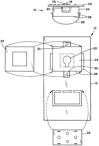
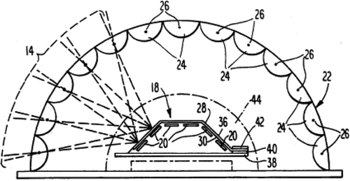
Myron and Konradi (Citation2001) invented an occupancy sensor (Patent No. US6222191 B1) in year 2001. This occupancy sensor has multiple sensor including a unique sensor case assembly and sensor mounting scheme. With the unique casing, the sensor can be adjusted to provide broader ultrasonic pattern coverage and focus infrared light ray from various directions. The occupancy sensor consists of a passive infrared lens to focus infrared light ray from various directions. A changeable PIR sensor masking scheme is used to allow customization of PIR sensor sensitivity pattern. The mask of this sensor consists of an oblong pattern mask, masks with 180 degree, 270 degree and 360 degree and they can be twisted up to 30 degree. The mounting scheme is also designed in such a way to allow the sensor to be mounted on walls and ceilings with different condition (Myron & Konradi, Citation2001). Figure illustrated the exploded view of the particular occupancy sensor.
Figure 24. Occupancy sensor of US6222191.
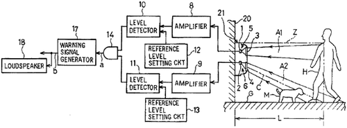
The usage of PIR sensor brings few advantages to the users. This includes improving the security systems. The devices is able to detect when someone is around the properties as his or her motion was detected. The signal is then send to the security system’s control panel to stay alert and wake alarms up when necessary. The signal can also be send to a local security stations to dial a sequence of phone numbers in order to provide a verbal alarms (Glidewell, Fun, & Witham, Citation1994). The usage of PIR sensor in lighting system can aids in saving a considerable amount of energy. The light will only be turned on whenever there is a motion detected. It has been estimated that for every 2.3 units of power produced, approximately a single unit of energy can be saved (Yavuz, Taşbaşi, Evirgen, & Kara, Citation1996).
The disadvantages of the sensor is related to its sensitivity and delay time. Sensitivity is the range that needs to be “seen” or detect by the sensor. The sensitivity need to be adjust according to the requirement by its user. If the sensitivity is large, the sensor may send a fake signal which will triggers a false alarm to the system. The sensitivity can be adjusted by adjusting an optical gain, pulse count, or electrical or optical sensitivity of the PIR sensor (Zakrewski, Citation2005). For the delay time, it is the period allowed for the sensor to keep the output “high”. Different sensor will have different delay time for the operations. Therefore, the delay time needs to be set precisely so that the sensor will be able to perform in the optimum condition and to be fully utilized.
A light sensor contains a major component, a photoresistor or light-dependent resistor (LDR). Photoresistor or LDR is a resistor that is sensitive to light and can be used as switch with based on the intensity of light. The resistance of the resistor will be increased if the light intensity that it received is decreasing. This features is known as photoconductivity. The characteristics of light dependent resistor allows it to be used in light-sensitive detector circuits or light and dark activated switching circuits. Photosensor or photodetector is another type of sensor that operated with the presence of light or other electromagnetic energy (Haugan et al., Citation2008). P-N junction inside the photodetectors will convert the light photons into current. With the absorbed photons, the photosensors are able to make electron-hole pairs in the depletion region. Temperature compensated solar light sensor, infrared light sensor and ambient light sensor are the types of light sensor that will be discussed.
5.3. Temperature compensated solar light sensor
Mandalakas invented a temperature compensated solar light sensor patent no. US 3480781. In this product, two solar cells that have the same features are mounted on a thermal equalizing plate. A temperature resistor is also mounted on the plate. The cells and the resistor are able to receive the same intensity of light and same temperature as they have the same physical location and construction. The use of two solar cells can ensure that the output variations of one cell cause by temperature difference is cancelled out by another solar cell. Both solar cells are operated under short-circuit conditions for good linearity of output with intensity. The short circuit consists of an emitter follower configuration controlled by an operational amplifier (Mandalakas, Citation1969) . Figure shows the isometric view and the circuit symbol of the solar light sensor.
Figure 25. Temperature compensated solar light sensor US 3480781.
5.4. Infrared light sensor
Watabe, Honda, Aizawa, and Ichihara (Citation2001) invented an infrared sensor patent no. US 6236046 in 2001. According to this invention, 2 infrared detecting elements are used. The first infrared element is mounted in a container through a supporting substrate while the second infrared element is also mounted in the container for the compensation of temperature difference. The second infrared element is shielded by the supporting substrate of the first infrared element from the incident infrared within the container. Any deterioration in the detecting various ambient temperature can be restrained by this arrangement without causing any hindrance to the compensation for the ambient temperature. This arrangement will also improve the sensitivity of the sensor to keeping it at high precision and the cost of building it is inexpensive Watabe et al. (Citation2001). Figure illustrates the sectional view of the respective infrared sensor.
Figure 26. Infrared sensor of US 6236046.
5.5. Ambient light sensor
An ambient light sensor patent no. US6396040 was invented in 2002 by Hill. In this invention, the light sensor is improved where it is able to distinguish between a natural light and an artificial ambient light. This technology is used in a vehicle system controller where it uses photo sensors that will responds differently towards the peak frequencies of natural light and artificial ambient light. There are two photodiode where the first one responds to the peak frequencies in the visible spectrum while the second sensor responds to peak frequencies in the infrared spectrum (Hill, Citation2002). By gathering the information of the light ray received, the control system will identify whether to turn on the lights or not. Figure shows the sectional view of the patented ambient light sensor.
Figure 27. Ambient light sensor of US6396040.
The light sensor has its advantages and disadvantages to its user. The sensor is relatively cheaper as compare to the PIR sensor. The circuit for setting the light sensor into a system is simpler compare to PIR sensor. Light sensor is suitable to be used in lighting system where it focus on turning the lights on during night time. The sensitivity of the sensor is therefore critical in applying it in this application. This will helps in saving the energy as the light is switched on only when it is necessary.
By measuring the light rays and identify whether it is necessary to switch on the circuit, the light sensor is only be able to function in a dark place or dark atmosphere. It is important to determine the environment for a particular environment and identify which type of sensor to be used. Failure in determining the condition may results in choosing a not suitable sensor to be used.
6. Lighting technology
Selecting a bright luminous and energy saving light sources will aid in producing an energy efficient power socket. Artificial lighting technology began to develop since nineteenth century. In 1809, Sir Humphrey Davey demonstrates an electrical discharge lighting using an open arc between two carbon rods which emits pure white and intense light. This idea was enhanced by Thomas Edison in patenting a carbon filament incandescent lamp in 1880. The first fluorescent lamp was on commercial sale by Artcraft Fluorescent Lighting Corperation in 1938. First quartz halogen lamp or tungsten halogen lamp was invented in 1957 and this was followed by the invention of first LED in 1962. In the latest invention, Ushio Lighting demonstrates the first LED filament light bulb in 2008.
6.1. Tungsten halogen lamp
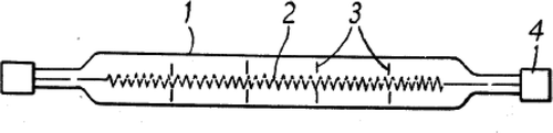
A halogen lamp, or in other terms as tungsten halogen lamp, is an incandescent lamp. It consists of a tungsten filament sealed into a compact transparent envelope that is filled with a mixture of inert gas and little amount of halogens. The halogen gas inside the bulb will produce halogen cycle chemical reaction by combining with tungsten filament that are heated. A carbon filament lamp was created using chlorine as halogen gas inside the lamp in 1882 and chorine-filled “NoVak” lamps were created in 1892 (Wallace, Citation2001). The use of iodine as halogen gas inside the lamp was proposed in 1993 and patented by General Electric in 1959 (Kane & Sell, Citation2001). In conventional tungsten lamps, the filament metal slowly evaporates and condenses on the glass envelope, leaving a black stain. The halogen then removes the deposited tungsten and puts it back on the filament.
A tungsten halogen lamp was invented by Westlund, Palmer, Audesse, and Huston (Citation1974). This halogen lamp has an aluminosillicate glass envelope with wedge base. The coil of wire used is molybdenum wires that passing through a pinch seal. The unstabilized tungsten coil filament are supported by clamp at each end. The lamp is filled with an inert gas, such as argon, nitrogen, krypton, or a mixture of halogen additive such as bromine, for example, in the form of hydrogen bromide. The lamp can also include a getter made from tantalum wire to be secure in the base pinch seal (Westlund et al., Citation1974). Figure shows the sectional view of this tungsten halogen lamp.
Figure 28. Tungsten halogen lamp patent no. US 3829729.
In an invention of James P. Keenan (patent no. US 4049988), the gaseous filled inside the tungsten halogen lamp is helium to prevent deposits forming on the wall surface of the tungsten lamp (Keenan, Citation1977).
A linear tungsten halogen lamp (patent no. US 4027189) was invented by Coaton in 1977. The linear tungsten halogen lamp is able to burn at any desired angle. The gas fillings selected are halogen or halogen-containing compound which require mathematically expression to satisfy this condition. If the mathematical proving part is accepted, the angles of the lamp when burning at the inclined angle is reduced to an acceptable level. The maximum degree of separation of the halogen can be calculated from the lamp parameters as a function of the thermal diffusion coefficient of halogen in the filling (Coaton, Citation1977). Figure illustrates the front view of the respective lamp.
Figure 29. Tungsten halogen lamp patent no. US 4027189.
Another type of tungsten halogen lamp (patent no. 3641386) was invented by Audesse, Griffin, Tartakoff, and Gutta (Citation1972). The lamps envelope is made up of hard glass which the upper part of it has a temperature gradient of approximately 200°C. When the lamp is heated, the halogen will react with the impurities in the tungsten to condense the halogen out non-regeneratively on the top of the envelope. The supporting conductors of the lamp are made to be small enough to operate at incandescence at the designed current compare to the larger diameter of supporting conductors used in normal incandescent lamp. The voltage drop due to the smaller diameter of supporting conductors is compensated by creating the filament coil that is able to operate at the desired temperature with lower voltage in a circumference occupy with bromine and krypton (Audesse et al., Citation1972). Figure shows the side view of the patented tungsten halogen lamp.
Figure 30. Tungsten halogen lamp patent no. US 3641386.
A glass halogen lamp (patent no. 5910707) was invented by Bell in 1999. Aluminisilicate glasses are used as glass envelope where they exhibit short wavelength transmission. These glasses exhibits up to 65% of light transmission at 340 nm for a thickness of 1mm. The transmission of light rays can be increased up to 83% at 340 nm for a thickness of 1 mm by reducing the iron level to 100ppm or less. By utilizing a thinner wall thickness at appropriate sections of the envelope together with reducing in the iron level, the short wavelength transmission can be improved and higher level of light output can be achieved (Bell, Citation1999). Figure shows the sectional view of the patented halogen lamp.
Figure 31. Glass halogen lamp patent no. US 5910707.
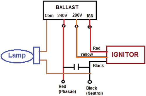
An electrical ballast is required in the circuit for tungsten halogen lamp to limit the amount of current flows. The device is placed in line with the load of the circuit. There is a variety types of ballast. It can be a simple combination of a resistor, inductor or capacitor to a complex combination that is widely used in compact fluorescent lamps and high-intensity discharge lamps. Ballast in used mainly when a load has its terminal voltage decline when current through the load increases. This continuous increasing of current will damage the power supply and caused it to fail (Ofer, Citation2012). Ballast is used to provide a positive resistance or reactance that will limit the current. Ballast is mainly used in a fluorescent lamp, a device with negative differential resistance (Nihal, Citation1998). A lighting source ballast utilizes switching and control technology to convert an alternating current (AC) phase modulated dimmer input voltage into an approximately constant driver current to illuminate the bulb (Melanson, Citation2010). Figure demonstrates the circuit diagram of a ballast in a lighting system.
Figure 32. The circuit diagram of an electrical ballast in lighting system.
6.2. Light emitting diode (LED)
LED or light emitting diode is a two-lead semiconductor device which will emits light when it is activated. When a desire voltage is supplied to the leads, electrons will recombine with electron holes within the device, releasing energy in the form of photons. The earliest LED was designed by Holonyak in 1962 which only emitted low-intensity infrared light (Massachusetts Institute of Technology, Citation2004; Okan & Baird, Citation2015) . The current LED design and product are more efficient than the incandescent lamp in terms of energy consumption and lifetime.
In Sakai and Kawamura (Citation1987) invention patent no. US 4698730, the light-emitting element of a LED is mounted on a lead frame, stem or substrate. The lens is made by resin through molding. A cap with peripheral surface with a hollow portion in the middle is made with light-transparent resin. It is mounted on the lens portion of the LED to form a parabolic surface. With this features, the LED can reflect the emitted light forwardly from the light emitting element. The light emitted from the side of light emitted element can be reflected forward as a parallel light with the peripheral shape of the cap. These emissions of light will increase the luminance of the LED (Sakai & Kawamura, Citation1987). Figure shows the sectional view of the respective LED.
Figure 33. Light emitting diode US 4698730.
An LED patent no. US6914267 was created by Fukasawa, Miyasshita, and Tsuchiya (Citation2005). This LED shows a different line up of components. The light emitting element of LED is mounted on a glass epoxy substrate. There is a resin seal member applied on the light emitting element to protect the surface side. Gallium nitride type compound semiconductor is used as the light emitting element and this will emit blue luminescence. A layer containing fluorescent material in placed on the back side of the LED. With this arrangement, the blue light emitted from the light emitted element is converted into a wavelength which white luminescence of high luminescent intensity is obtained (Fukasawa et al., Citation2005). Figure ) shows the sectional view of the patented LED whereas Figure ) illustrates the exploded view on the how the light emitting element is placed on the base plate.
Figure 34. Light emitting diode patent no. US6914267.
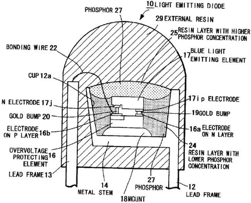
Nakada, Aoki, Oba, and Kagiwada (Citation1972) invented another type of LED (Patent No. US6774401) in 2004. This invention aims in improving the intensity of the light emitted from LED using a simple configuration. An electrode terminals, a LED chip, a reflector, an enclosing resin and a wavelength conversion material are used in the configuration. The reflector is in a bowl shape to reflect the light emitted from LED chip to the opening. A LED chip is connected to the electrode terminal. The density of the wavelength conversion material mixed into the enclosing resin is larger at the bottom of the junction surface of the LED chip than at the top. The wavelength conversion material contains enclosing resin which absorbs the light emitted from LED and emits the light with longer wavelength as compare to the light it absorbed (Nakada et al., Citation1972). Figure shows the sectional view of the LED where the electrode terminal is placed on the centre of the LED.
Figure 35. Light emitting diode patent no. US6774401.
An LED was invented by Takekuma (patent no. US 6850001) in 2005. This LED has no fluctuations in optical properties and has good sealing properties. Thus, it is relatively simple to produce this LED. The LED has a cup shape base where the light emitting element is place in the centre of the base. A resin material is also used to fill into the cup part. A transparent lens member is placed on the top of the cup shape base to focus the light emitted from the LED. A layer of fluorescent material is applied to the convex surface of the cup shape base which convert the wavelength of some of the light emitted. By attaching the lens member to the cup shape base, the inner convex face will deform the resin material and excess resin material can be pushed to the outside (Takekuma, Citation2005). Figure shows the sectional view of the respective LED.
Figure 36. Light emitting diode patent no. US 6850001.
The following LED was invented Takahashi et al. (Citation2004) . The LED contains a layer of scattering materials with light guiding to receive the light emitted from light emitting material. The scattering layers with irregular light guiding will reflects and scatters the emitted light. The scattered light will lead to a fluorescence emitting layer which form a transparent binder that contains phosphor material. The refracted light has high optical density and it can be radiated from the whole fluorescence emitting layer. With this properties, uniform light with desired colour can be radiated with high efficiency from LED (Takahashi, Citation2004). Figure shows the sectional view of the patented LED.
Figure 37. Light emitting diode patent no. US6791116.
The comparisons between LED light bulb and tungsten halogen light bulb are shown in Table .
Table 4. Energy efficiency comparison of bulbs (Ayan, Citation2017)
From Table , LED bulbs shows a longer life spans which is 10 to 50 times longer compare to tungsten halogen bulbs. Besides that, the consumption of electricity for LED bulb is comparatively low compare to Tungsten halogen bulb.
Table shows that both bulbs does not contain toxic material such as mercury. However, both bulbs are under Restriction of Hazardous Substances (RoHS) compliant which means they contains restricted substances in this case is lead. Therefore, these bulbs need to be disposed carefully to avoid pollutions. Table also shows that the carbon dioxide emissions from LED bulbs is lower compare to tungsten halogen bulbs.
Table 5. Environmental impact comparison of bulbs (Ayan, Citation2017)
Table shows that both bulbs are insensitive to temperature and their function will not be affected by any changes in temperature. These bulbs are sensitive to humidity as the humidity environment may affect their performance. The durability of LED bulbs is better as compare to tungsten halogen bulbs. Tungsten halogen lamp will fail and spoiled more frequently than LED bulbs. LED will emit more heat than tungsten halogen bulb.
Table 6. Specific features of bulbs (Ayan, Citation2017)
Table shows that the higher the light output, the more energy input is required. However, LED bulb consumed the electrical power in a lower scale compare to tungsten halogen bulb.
Table 7. Power and lumen comparison of bulbs (Ayan, Citation2017)
7. Summary of review works
From the literature review analysed, a few important points can be highlighted which is as followed:
Standards and codings must be strictly followed in order to fabricate a safe product for the consumer;
Material selection is crucial to avoid accidents such as short circuit and material breakdown;
It was found that universal adapter was invented in 1982 by Rumble to cater the fixtures of plugs in various country;
Sensors is used as a switch that will only switch certain appliances on when the particular gesture is detected;
LED is a better choice for lighting system as it has higher luminescence and more energy efficient
SnapPower© is a new revolution of sockets which combines a wall socket together with a sensor lighting system.
Through literature survey and through the best of knowledge, it is understood that there are numerous ways one may design an adapter fusing other sensors and lighting technology into a single product. This is namely to incorporate the multi-feature concept within a single product which benefits the user. Hence, the following section proposes new research pathways which may be carried out to tackle this.
8. Proposed future works
Based on the design review works conducted on multipurpose power socket for home application, we can clarify the fact that the idea of smart multipurpose power socket is novel and new research pathways can be achieved. As such, certain research questions worthy of exploration may include (but are not limited to) the following:
In what way does the safety features of the sockets regarding BS 546 and BS 1362 such as fuse-link be applied into the future design work?
Is there any green material that can be used to substitute the current material used without overlooking the required properties at the same time provide further enhancement to the future work?
Can the concept of using SnapPower© be implemented according to BS 546 and BS 1362 standard?
How can one improve energy efficiency effectively by fusing different types of sensors and lighting technology into a single home adapter socket?
How can the safety features of an electrical adapter for home application be enhanced without compromising its features?
| List of abbreviations | = | |
| Abbreviations | = | Descriptions |
| BS | = | British Standard |
| LED | = | Light Emitting Diode |
| PIR | = | Passive Infrared Resistor |
| ISO | = | International Standard Organization |
| AC | = | Alternating Current |
| MS | = | Malaysia Standard |
| IEC | = | International Electrotechnical Commission |
| SIRIM | = | Standard and Industrial Research Institute of Malaysia |
| IACS | = | International Association of Classification Societies |
| DC | = | Direct Current |
| USB | = | Universal Serial Bus |
| IR | = | Infrared Ray |
| PC | = | Printed Circuit |
| LDR | = | Light Emitting Diode |
| RoHS | = | Restriction of Hazardous Substances |
| CO2 | = | Carbon Dioxide |
Additional information
Funding
Notes on contributors

Chin jie Wong
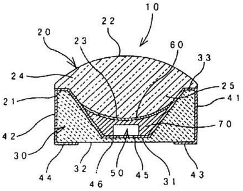
Chin Jie Wong studies Bachelor of Engineering (Honours) Mechanical at the Faculty of Engineering and Technology, Multimedia University, Melaka Campus, Malaysia. His research interests are in the field of Mechanical Mechanisms, Electrical and Electronics. Together with his mentor, Umar Nirmal, they worked extensively on the design and development of smart multipurpose power socket for home application. The prototype consists of a type G 240V power socket that consist a sensor for smart lighting system. The prototype is build based on a “plug and play” concept and its targeted for home applications. With this invention, energy wastage can be minimized while hazardous and low level of illumination can be overcome.
References
- Audesse, E. G. , Griffin, R. M. , Tartakoff, A. , & Gutta, J. J. (1972). Tungsten halogen lamp US3641386.
- Ayan, O. (2017). Comparison of lighting technologies in residential area for energy conservation .
- Batko, T. J. , & Baldwin, J. I. (2000). Temperature and passive infrared sensor module. U. S. Patent 6082894 .
- Batko, T. J. , & Eckel, D. P. (1998). Temperature and passive infrared sensor module. U. S. Patent 5772326 .
- Bell, D. A. (1999). Tungsten halogen lamp US 5910707 .
- Black, B. (2010). Workshop processes, practices and materials (Vol. 4, 4th ed., pp. 20–25). Routledge Taylor and Francis Group.
- Coaton, J. R. (1977). Tungsten halogen lamp US4027189.
- Drewnicki, R. (1995). Electrical adapter. U. S. Patent 5474464.
- Energy Commission Malaysia . 2009. Information Booklet 2009 edition .
- Faraday, M. (1832). Experimental researches in electricity. Philosophical Transactions of the Royal Society of London , 122, 125–162. doi:10.1098/rstl.1832.0006
- Fukasawa, K. , Miyasshita, J. , & Tsuchiya, K. (2005). Light emitting diode US 6914267.
- Fungal, I. N. , & Brody, S. (1996). Copper and copper alloys (Vol. 72). Springerlink.
- Gardziella, A. , Pilato, L. A. , & Knop, A. (2000). Phenolic resins: Chemistry, applications, standardization, safety and ecology (2nd ed.). Springerlink.
- Gilleo, K. (2004). Area array packaging processes: For BGA, flip chip and CSP (Vol. 2, pp. 157–171). McGraw Hill Professional.
- Glidewell, W. E. , Fun, E. F. , & Witham, M. J. (1994). Security system. U. S. Patent 5319698 .
- Haugan, H. J. , Elhamri, S. , Szmulowicz, F. , Ullrich, B. , Brown, G. J. , & Mitchel, W. C. (2008). Study of residual background carriers in midinfrared InAs∕GaSb superlattices for uncooled detector operation. Applied Physics Letters , 92, 071102. doi:10.1063/1.2884264
- Hesse, W. (2004). Phenolic resins in Ullmann’s encyclopedia of industrial chemistry . Wiley-VCH.
- Hill, J. W. (2002). Ambient Light Sensor Us6396040 , 2(16), 4–9.
- I. British Standard . (1995). 13 A plugs, socket-outlets, adaptors and connection units. British Standards Institute , 3(1).
- International Organization for Standardization . (2007). Guidance notes for the electrical products (Safety) regulation .
- Kane, R , & Sell, H . (2001). Revolution in lamps: a chronicle of 50 years of progress (2nd ed.). The Fairmont Press, Inc.
- Keenan, J. P . (1977). Tungsten halogen lamp , US4049988 (pp. 3–5).
- Kondo, M. , Mikio, S. , Morimoto, M. , & Kayanoki, K. (1987). Passive infrared detector. U. S. Patent 4672206 .
- Lee, A. (1992). Universal adapter. U. S. Patent 5159545 .
- Lee, A. (1998). Easy operable and universal adapter (vol. 113).
- Lee, C. S. , & Li, S. C. (2001). Universal electric adapter. U. S. Patent 6328581 .
- Liaw, D. J. , Wang, K. L. , Huang, Y. C. , Lee, K. R. , Lai, J. Y. , & Ha, C. S. (2012). Advanced polyimide materials: Syntheses, physical properties and applications. Progress in Polymer Science , 3(2).
- Mandalakas, J. N. (1969). Temperature compensated solar cell light sensor US3480781 .
- Massachusetts Institute of Technology . (2004). Inventor of long-lasting, low-heat light source awarded 2 015 000 MYR Lemelson-MIT Prize for Invention .
- Melanson, J. J. (2010). Ballast for light emitting diode light sources. 2(12). US7852017B1.
- Muller, K. , & Allemann, M. (2003). Passive infrared detector. U. S. Patent 6559448 .
- Myron, D. D. , & Konradi, V. A. (2001). Occupancy sensor. U. S. Patent 6222191 .
- Nakada, K. , Aoki, D. , Oba, H. , & Kagiwada, M. (1972). Light emitting diode US6774401.
- Nihal, K. (1998). Power electronics design handbook.
- Noguchi, M. (2007a). Passive infrared sensor. U. S. Patent 7170060 B2 .
- Noguchi, M. (2007b). Passive infrared sensor. U. S. Patent 7196330 .
- Ofer, A . (2012). Optoisolation circuits: Nonlinearity applications in engineering . World Scientific.
- Okon, T. M. , & Biard, J. R. (2015). The first practical LED.
- Philips, R. P. , Fischer, D. , & Fyke, S. (2013). Universal adapter with interchangeable plugs. U. S. Patent 6845023 .
- Rumble, C. S. (1985). Unitary electrical plug with multiple inlets and voltage converter. U.S. Patent 4543624 .
- Rumble, C. S. (1986). Electrical connectors. U. S. Patent 4626052 .
- Sakai, H. , & Kawamura, T. (1987). Light emitting diode US 4698730.
- Saudi Standards, Metrology and Quality Org . (2010). Plugs and Socket-Outlets for Household and Similar Purposes-Safety Requirements and Test Methods 250 V/13 A .
- Smith, J. (2014). Active cover plate. U. S. Patent 8912442 .
- Smith, J. C. , Watkins, S. D. , Dietz, P. , Oyler, B. , Bagirov, Y. , Tung, J. , & Bates, C. L. (2015). Active cover plate. U. S. Patent 2015/0075836 .
- Takahashi, Y. , Fukumoto, S., Arakane, K., Hirano, A., Hadame, K., Obara, K., ... Yamanouchi, Y. (2004). Light emitting diode US6791116 .
- Takekuma, A. (2005). Light emitting diode US 6850001 .
- Talbot, F. W. (1941). Manufacture of melamine-aldehyde condensation products. U. S. Patent 2260239 .
- Techakittiroj, K. (2008). Electrical plug and outlet for the DC distribution system in buildings .
- Tom, E. (1992). Passive infrared detector. U. S. Patent 5107120 .
- Tomooka, H. , & Sugimoto, T. (1997). Passive-type infrared sensor system for detecting human body. U. S. Patent 5703368.
- Wallace, H. (2001, November/December). A different kind of chemistry: A history of tungsten halogen lamps. IEEE Industry Applications Magazine.
- Watabe, Y. , Honda, Y. , Aizawa, K. , & Ichihara, T. (2001). Infrared sensor US 6236046.
- Westlund, A. E. , Palmer, L. H. , Audesse, E. G. , & Huston, L. S. (1974). Tungsten Halogen Lamp US 3829729.
- Wong, M. P. K. (2005). Electrical adapter. U. S. Patent 6942508 .
- Yavuz, S. O. , Taşbaşi, A. , Evirgen, A. , & Kara, A. (1996). Motion detector with PIR sensor usage areas and advantages (pp. 7–16).
- Zakrewski, D. S. (2005). Automatic sensitivity adjustment on motion detectors in security system. U. S. Patent 2005/0128067 .
- Zi-Bo, Z. B. , Man, M. , Chang-Zheng, C. Z. , & Ming, Z. (2011). Study in plug-socket loose contact tests and fire trace identification technology thereof. Procedia Engineering , 11, 360–368. doi:10.1016/j.proeng.2011.04.670