
 ?Mathematical formulae have been encoded as MathML and are displayed in this HTML version using MathJax in order to improve their display. Uncheck the box to turn MathJax off. This feature requires Javascript. Click on a formula to zoom.
Abstract
The growing consciousness in health, biomedical research area is becoming most sought-after to develop or design medical devices by bringing biomedical researchers and clinicians to solve many health issues. Biomedical electronics is the endorsement and resolution of many techniques in engineering powered biology and medicine. The medical imaging accounts the design and development of electrophysiological monitoring devices to examine the whole human body for proper diagnosis. The biomedical signals are low amplitude, low frequency, are to be amplified in the range of millihertz to kilohertz while rejecting the dc offsets, created a tremendous demand amongst neuroscience researchers and clinicians. In this design capacitive feedback, neural signal recording amplifier is designed using folded cascode operational transconductance amplifier (OTA). The neural amplifier uses an AC coupled input signal to segregate the DC offset voltages generated at electrode-nerve interface due to chemical reaction and AC coupled input also represses the flicker noise. A large resistor, implemented using two series MOS devices as pseudo resistors, used in parallel to capacitive feedback to exploit device off-resistance for DC feedback normalization. This article presents a bulk-driven, buffer-biased, gain-boosted amplifier for biomedical signal is designed using 90 nm CMOS technology to capture signal activity. The bulk-driven folded cascode topology is used to design amplifier, which has reduced threshold voltage and supply voltage by consuming half the power of the conventional gate driven counter parts. The proposed and designed bulk-driven folded cascode operational transconductance amplifier (BD FC-OTA) achieved a gain of 81 dB, 39 nV/√ Hz is the recorded noise characteristics by consuming less power of 2.5 µW. The Wilson current mirror method has benefited the amplifier to enhance the gain and compensation capacitor with series resistor realized by MOSFET device is used in designing 1V powered buffer biased BD FC-OTA for biomedical applications. The layout of a proposed bulk-driven folded cascode amplifier is designed using Cadence Virtuoso has a dimensions of 17.255× 35.5μm.
PUBLIC INTEREST STATEMENT
The growing consciousness in health, biomedical research area is becoming most sought-after to develop or design medical devices by bringing biomedical researchers and clinicians to solve many health issues. This research article depicts the design of low power and high gain amplifier to amplify the collected vital information from patients using neural recording systems. The proposed research work can also solve and help non-government and government institutions to ameliorate health coteries and individuals in making a spotlight on innovative and electrifying research area of biomedical electronics. We designed a high gain low noise amplifier for recording the neural signals from human body. This high gain- boosted amplifier can be used in designing and developing neural recording systems like EEG, ECG, ECoG, ENG etc. This research work mainly aims to instigate amplifiers which are the core unit to capture electrophysiological signals for all biomedical wearable devices to communicate and to solve set of impediments regarding patient monitoring in benefit of humanity.
1. Introduction
The expeditious growth of portable and miniature devices, escalated demand for denser integrated circuits (ICs) that necessitates low power and low voltage CMOS circuit designs (Raikos & Vlassis, Citation2010). In contemporary CMOS process, the reduction of aspect ratios (or) dimensions, necessitates dwindle of the allowable supply voltages. The development of this type of low power, low voltage ICs facilitated the interfacing between electronics and biomedical applications. Battery-maneuvered equipment in biomedical electronics engineering like hearing aids, ambulatory brain machine interface systems, insulin pumps require low voltage and low power design in submicron levels (Raj, Sharma, Jasuja, & Gard, Citation2010). Biomedical signals (or) physiological signals are of low frequency and small amplitude which are processed with ample large time constant (= RC) and passive elements like capacitors less than 5 pF. The traditional analog circuits like operational amplifiers (op-amps) require power supply voltages of leastwise magnitudes of large threshold voltages and imperative signal voltage swings of NMOS (or) PMOS devices (Zuo & Syed, Citation2013). Many novel techniques are needed to scale down the threshold voltage to get benefitted from devices in deep sub-micron CMOS process with counter fronting the noise immunity. The biomedical engineering field is robust in adapting the portable and low power devices to monitor patients continuously (Raj et al., Citation2010). The continuous and prolonged time period monitoring by biomedical devices demands the frequent small-sized non-replacement batteries and weightless machines with very low power consumption and low voltage operation. The traditional CMOS gate-driven op-amps are scant for sub-micron voltage supplies due to restricted common mode range of input signal. Various techniques are developed for low voltage and low power consumption (Carrillo, Torelli, P-Aloe, Valverde, & D-Carrillo, Citation2010; Sharan & Bhadauria, Citation2017; Sharan, Chetri, & Bhadauria, Citation2018) integrated circuit design without enlisting the exorbitant low threshold voltage devices such as level shifting techniques, floating gate (Rodriguez-Villegas, Yufera, & Reuda, Citation2004), sub threshold designs (Cotrim & Ferreira, Citation2012; SamadSheikhaei, Citation2019) and bulk-driven MOSFETs (Szczepanski, Pankiewicz, Koziel, & Wojcikowski, Citation2015), pseudo-differential approach (Lo & Hung, Citation2007) and flipped voltage approach (Carvajal et al., Citation2005). Among above-mentioned literature; bulk-driven technique and sub threshold operation are best suitable choice for low power, low frequency, and low voltage biomedical solicitation.
Bulk driven (BD) is a promising technique to deal low voltage, low threshold demanding compatible CMOS devices (Khateb, Biolek, Khatib, & Vávra, Citation2010), it also provides large voltage signal swing (Ferreira, Pimenta, & Moreno, Citation2007). It reduces the power consumption compared to conventional gate driven technique but has increased input-referred (IR) noise because bulk source trans-conductance (gmb) in BD devices is 3–5 times smaller than gate driven source trans-conductance (gm) (Sharan & Bhadauria, Citation2016).The designing of a low voltage, low power amplifier for the low frequency biomedical signals like EEG, ECG, EMG etc is carried by operational trans-conductance amplifier (OTA); which is impetus voltage-controlled current source (VCCS) building block for biomedical devices with high output impedance. Biomedical signals vary in their signal frequencies of up to few kHz and amplitude ranges from 1 µV to 500 mV (Bano, Narejo, Shah, & Syed, Citation2018). Different design correction and efficient techniques are developed and reported in recent literatures to achieve good trans-conductance of few nA/V and also to have enhanced linear range like source degeneration technique (Worapishet & Naphaphan, Citation2003), input attenuation method (El Mourabit, Lu, & Pittet, Citation2005), adaptive biasing method (Razaei & Azhari, Citation2015). And other techniques like feed forward technique (Kim, Kim, & Nam, Citation2015), Bulk-driven technique (Moreno, Baruqui, & Petraglia, Citation2015), current division technique and non-linear term cancellation (Lee & Cheng, Citation2009), current summing method (Lee & Song, Citation2019) are developed and discussed to cancel OTA’s third-order non-linear component, to improve linearity and control the cancellation factor and also to have improved linear range (up to ± 0.4 V) under 1V supply, respectively.
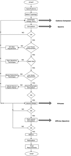
The design methodology and optimization of all required parameters for a biomedical amplifier is exhibited neatly using flow charts in Figures and . Figure depicts a research methodology design process that is followed for a good successful design flow to have better knowledge in designing a better amplifier for biomedical applications. Based on these steps followed in research methodology flow, a new methodology is proposed to design a bulk-driven folded cascode trans-conductance amplifier (OTA) for biomedical applications, which is summarized in Figure .
Figure 1. Flow chart of research methodology
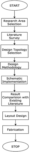
Figure 2. Flow chart of bulk-driven folded cascode trans-conductance amplifier design
In this research article, low voltage, power efficient, high gain amplifier is designed for bio-medical application, which can avoid regular battery replacement in portable bio-medical devices; by working continuously for prolonged time periods. The designed amplifier have improved linearity with reduced distortion at signal output and achieved high performance gain. The bulk-driven folded cascode topology is used to design amplifier, which has reduced threshold voltage and supply voltage by consuming half the power of the conventional gate driven counter parts.
2. Basic human electrophysiology
Human body has an intricate network which is spread across the body and is controlled by the centers in the Brain and the Spinal cord. It is this nerve network which conveys the action commands from the control centers and in return gathers feedback information from various parts of the body via electro-chemical mechanisms. The unit of this elaborate nerve network is called a neuron. Neuron is a cell which has a cell body, dendrites, and an axon. Neurological and psychiatric disorders might be due to changes in inter-neuron information transfer and changes in the excitability of the neurons. Epilepsy is an example of a disease due to abnormal neuronal excitability. The information is transferred between neurons in the form of electrical signal which result from the flow of chemical ions across the cell membrane through ion channels. There are broadly two types of ion channels; they are leakage channels and voltage-gated channels. The leakage channels are open at rest and influence the cellular resting membrane potential. Voltage-gated channels on the other sideopen and close rapidly creating rapid signals called action potentials. These action potentials are generated near cell body and are transmitted along the axon till the nerve terminal without much decrement due to myelination of axon. At the nerve terminal, the action potential-induced depolarization opens voltage-gated calcium channels, which release chemicals called neuro-transmitters outside the neuron. When the neurotransmitter binds to another neuron it alters its excitability and thereby transferring the information, which is further propagated till its intended end site.
2.1. Resting membrane potential and properties of a passive membrane
Cell membranes are selectively permeable to K+(Potassium) ions at rest which leads to a less negative (depolarized) membrane potential and the electrical gradient driven influx is slowed down. Inside the neuron K+ concentration increases to the levels of 100 mM while outside it is only 2–6 mM, this sets up a chemical gradient. These electrical and chemical gradients acting in opposite directions become equal at a specific membrane potential (for K+, it’s around 90 mV). This is called the equilibrium potential or Nernst potential for K+(CitationSadock et al.). Its formula is EK = (RT/zF)ёln([K]o/[K]i) where R is the ideal gas constant, T is temperature in Kelvin, z is the valence of the ion, F is the Faraday’s constant, [K]o and [K]i are the K+ concentrations outside and inside the cell. However, cells are permeable to many other ions like Calcium (Ca2+), Sodium (Na+), Chloride (Cl−) etc. Therefore, the true resting membrane potential is the average of the equilibrium potentials of various individual ions, which are flowing across the membrane in that particular cell. If we think of a cell membrane as an electrical circuit, then ion channels can be thought of as variable resistors. These channels are selective to which ions can pass through them, have a degree of conductance i.e. the relative ease with which ions pass through them. Transmembrane voltage drives ion flow through the ion channels which results in current. In this scenario, the Ohm’s law can be depicted as follows: Iionic = g(Vm-Erev), where Vm is the membrane potential, Erev is the equilibrium potential for the passing ions and Vm–Erev is the driving force. Apart from this transmembrane current, some current must be used to change the membrane capacitance (Cm), this capacitive current is depicted as: Icap = Cm (dV/dt) that is the capacitive current during changing voltage over time. The total current across a membrane at any given time is the sum of Icap and Iionic. Figure depicts the distribution of various chemicals like Na+, K+, Ca2+, and Cl— and current direction across the cell membrane (CitationSadock et al.). These neurons using electrical signals will determine the brain’s local and network properties and result from the flow of ions across cell membranes through macromolecular pores called ion channels.
2.2. Action potential and properties of membrane in active state
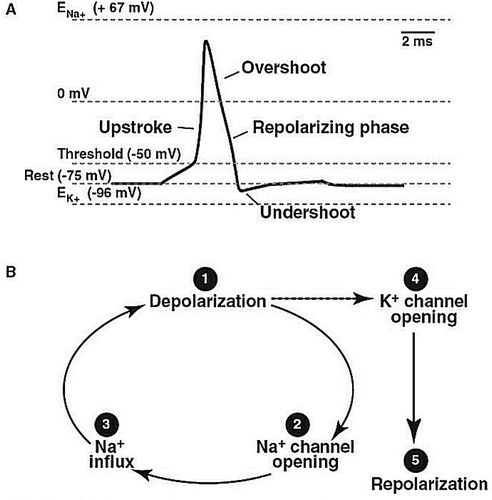
When neurons depolarize, Na+ (sodium) channels rapidly open and shift the membrane potential towards the equilibrium potential of sodium. As leakage channels are open at rest, there is a balance between leakage currents and Na+ channels opened at depolarization, but at a specific point, Na+ current exceeds the leakage current, membrane potential at this state is called the threshold potential. However, as Na+ depolarization opens voltage gated K+ channels; the membrane potential overshoots 0 mV and then rapidly returns to resting membrane potential after a transient undershoot. This rapid change occurs over several milliseconds and is called as an Action potential (or commonly as Sodium spike) and this propagates along the length of the axon. At the axon terminal, the spike provides Ca2+ opening depolarization and the resultant release of neurotransmitters which excite another neuron and thereby communicating information (Sadock et al., Citation0000). Figure depicts the depolarization and repolarization wave in a nerve cell (Sadock et al., Citation0000).
Figure 3. Distribution of various chemicals like Na+, K+, Ca2+, and Cl—and current direction across the cell membrane. These neurons using electrical signals will determine the brain’s local and network properties and result from the flow of ions across cell membranes through macromolecular pores called ion channels (CitationSadock et al.)
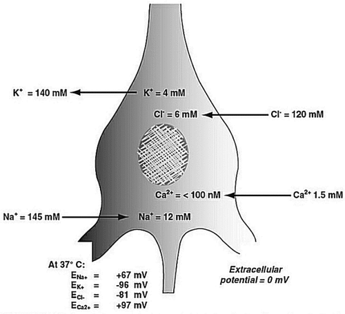
Figure 4. Depolarization and repolarization wave in a nerve cell (Sadock et al., Citation0000). (a) Recorded neuronal action potential. (b) Action potential sequence events
3. Bulk-driven technique for bio-medical signal amplifier
Bulk-driven technique was first proposed in (Guzinski, Bialko, & Matheau, Citation1987); whose operation is akin to FET (Blalock, Allen, & Rincon-Mora, Citation1998). The channel current in BD MOSFET is attuned by changing bulk source junction potential (VBS) when inversion layer is formed beneath the gate terminal of MOSFET due to sufficient gate-to-source biasing voltage (Zuo & Islam, Citation2013). The operational tans-conductance (OTA) majorly dissents in two ways from widely used amplifiers: 1.The gain of an OTA can by varied by bias current supplied. 2. The output signal in OTA is a current. Therefore, OTA is widely adopted for analog signal processing applications. The OTA design, implementation, and controlling do not require external feedback. Transistor used to design OTA is a four terminal device producing output current on triggering differential voltage input. The relationship between input-output signals of OTA is given by
Where V1, V2 are input signals, gm is the gate trans-conductance of OTA and Iout is the output current.
The operational characteristic of the BD and gate triggered NMOS devices are depicted in Figure and (Raj et al., Citation2010). It is reconnoitered that gate triggered NMOS devices in active region needs minimum threshold voltage of approximately 0.375 V; whereas BD NMOS will be in active region with even zero input biasing voltage at bulk of device, which behaves as depleted NMOSMOSFET. In BD technique; input voltage signal is applied to the bulk of input devices. BD devices are operated at low supply voltage to amputate the threshold voltage from the signal path. To assist low power and low voltage supply, BD is preferred over gate-triggered MOS. The linearity of an OTA without extra power-dissipation can be ameliorated by using BD transistors, which provide innate signal attenuation. The increase in linearity trade off with noise, the input- referred noise is increased.
Figure 5. High output impedance low-voltage current mirror (Raj et al., Citation2010)
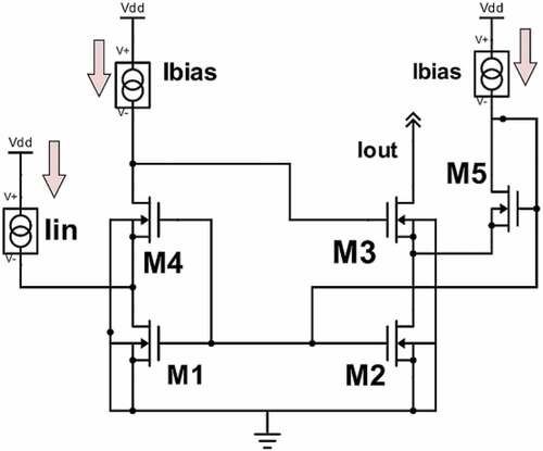
Figure 6. High-swing Wilson current mirror (Raj et al., Citation2010)
The gm and gmb relationship of the BD transistors are given by
Where CBC is total bulk channel capacitance and is given by
Where Cj is zero bias junction capacitance and is given by
The output conductance (g0) and output resistance (r0) of BD devices are given by
The unity gain frequency is given by
Where CBS is bulk source capacitance and CB–sub is bulk substrate parasitic capacitance
The large signal model equation of BD MOSFET is given by (Sarin Vijay & Moni, Citation2018)
For
For
Where
And
The BD MOSFETs’ small signal bulk trans-conductance is given by:-
The BD Cascode configuration is used to improve current matching in current mirror and to increase the output impedance. The BD current mirrors used to eliminate the large voltage drops in input devices.
3.1. Sub threshold device performance
The current in the weak inversion region is an exponential ramification of the input voltage.
The MOSFET drain to source current (IDS) for the sub threshold region is given by.
Where
Where IS is the characteristic current ⇒, nP is the slope factor in weak inversion, VGS, VBS, and VDS are gate, bulk, and drain voltages, respectively,
is threshold voltages at VBS = 0, VT =
that is thermal voltage, K is Boltzmann’s constant, q is electric charge.
The transistor will enter into saturation region when
The trans-conduction of the MOSFET gate terminal is given by
The gate trans-conductance (gm) of MOSFET is a function of drain current (ID) and ; the bulk terminal trans-conductance of the transistor is given by
EquationEquation (18)(18)
(18) depicts that gmb is a function of Fermi potential
and body effect coefficient
.
4. Noise analysis of CMOS for bulk-driven devices
The ubiquitous CMOS design is escalated the demand for fastidious low power, low noise features, which in turn increases obstruction to achieve high signal to noise ratio. The bio-medical operated signals lead to increase in noise on reducing the device size.
The dominant sources of CMOS device noise are to be superintended to design front end amplifiers for bio-medical applications. The dominant noise sources are categorized as (i) Flicker Noise, (ii) Shot Noise, (iii) Thermal Noise, (iv) Bulk-driven Noise, (v) Avalanche Noise, and (vi) Burst Noise. The spectral density, that is noise voltage (or) noise current per root hertz , specifies the noise parameter in MOSFETs.
4.1. Flicker noise
It is also called as noise randomly at
interface and gate-oxide area. The surface currents of MOSFET are highly susceptible to interface defects which produce high
noise. The flicker noise can be modelled by gate terminate MOSFET in series with voltage sources.
The noise (or) flicker noise of MOSFET is given by
Where K = 10–25 V2F
4.2. Shot noise
This noise is resulted due to the random charge crossing across potential (or) voltage barrier. The instantaneous current is defined as composition of average large number of random current pulses. The average of shot noise is mean square value given by
Where df is differential frequency, q is 1.62 x 10⁻¹⁹C and qID is current power density in .
4.3. Thermal noise
It is the noise because of MOSFET and resistors, generated by channel. The noise long channel MOSFETs in saturated region is modeled by current source between source and drain terminals. The Power Spectral density is given by
Where
4.4. Bulk-driven noise
The bulk-driven approach is varied from the gate driven by gain factors, which implicate the channel noise at the input. The additional thermal noise is also because of bulk sheet resistance of bulk-driven devices. The Bulk noise of MOSFET is given by
Where Rbi is ith gate channel effective series bulk resistance, Rgiith series gate-metal effective resistance and is
.
4.5. Avalanche noise
The Avalanche noise is produced due to the reverse break down operation of PN junction of MOSFET. The burst and Avalanche noise are less hazardous, so they can be obliterated.
4.6. Burst noise
It is mainly ascribable to the deformity in heavy ion implants and semi-conductor materials. It is also known as popcorn noise because of popping sound it makes during signal recording.
5. Bulk-driven folded cascode amplifier for bio-medical signal amplification
5.1. Circuit description
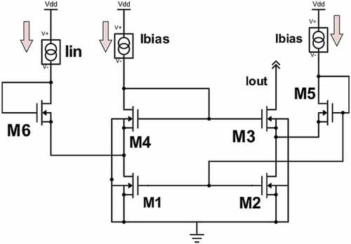
In this article, capacitive feedback neural signal recording amplifier is designed using folded cascode operational transconductance amplifier (OTA). The neural amplifier uses an AC coupled input signal to segregate the DC offset voltages generated at electrode-nerve interface due to chemical reaction and AC coupled input also represses the flicker noise. A large resistor, implemented using two series MOS devices as pseudo resistors, used in parallel to capacitive feedback to exploit device off-resistance for DC feedback normalization (Kim & Cha, Citation2018b). The pseudo resistor occupies smaller area by providing a large resistance. The miller capacitances (C1and C2) are used to filter the voltage offsets between buffer-biased stage and output stage (Lee & Song, Citation2019). The bulk-driven technique capacitates the low voltage signal to the input terminal of amplifier, which provides the benefits of threshold voltage. The bulk-driven folded cascode topology is used to design amplifier which has reduced threshold voltage and supply voltage by consuming half the power of the conventional gate driven counter parts. Figure shows the block diagram of bulk-driven FC amplifier. It is designed with the bulk-driven FC trans-conductance amplifier using capacitive feedback topology; enabling the gain setting and here mid band gain is enumerated by the ratio of input capacitor (C1) and feedback capacitor (C2). Figure presents the proposed bulk-driven folded cascode trans-conductance amplifier (OTA). The bulk terminal of input devices of the folded cascode amplifier is fed by biomedical low frequency signal to ease the wide input common mode signal range; to eradicate the curbs of the threshold voltage. The ground or zero voltage terminal is biased to the gate terminals of the input bulk devices to allocate required DC voltage biasing. Bulk-driven Fold Cascode (FC) amplifier has four stack transistors to achieve the high output resistance. The mismatch problem of MOS transistors threshold voltage, which may forefront the bias current disparity in the cascode arm is resolved by the negative feedback configuration in the block diagram. An offset voltage is established between the input signal terminals of trans-conductance amplifier by the negative feedback which avenues the current beck into the input terminal (Agrawal & Sankaran, Citation2017) branch. The low pass cut off frequency signal is adjusted at high value to reinforce the action potential signals. The sub Hertz high pass cut off signal is resolute by; where RF is high-valued pseudo resistor for MOS device for area competence attainment Kim and Cha (Citation2018a).
Figure 7. Block diagram of bulk-driven folded cascode amplifier (Sarin Vijay & Moni, Citation2018)
Figure 8. Proposed bulk-driven folded cascode amplifier
Folded cascode trans-conductance (FC—OTA) amplifier is the most widely used amplifier topology due to its large output signals swing and high gain characteristics. Large bulky input transistors are used for bulk-driven amplifier to ameliorate the recital of flicker noise and less thermal noise obtains low power consumption in input devices in weak inversion region. The greater mobility NMOS differential transistor pair is used to design the input stage of FC OTA to enhance the trans-conductance of the input device to ameliorate the gain, UGB and reduced noise characteristics. The conventional folded cascode OTA consumes high power, so input signal is triggered to the bulk of the MOS devices, which reduces the power consumption to the almost half of the conventional FC OTA topology. The continuous abate in the CMOS device technology, not reduced the threshold voltage at the pace the supply voltage has got reduced. Therefore, the input signal voltage at the gate has become equal (or) more than the supplied voltage which in turn violate the saturation conditions of MOSFET. To repress this muddle, input is applied to the bulk terminal instead of the traditional gate terminal of MOSFET. The cascading technique is used at devices to achieve high gain, by producing large output impedance (Mythry & Moni, Citation2018). The first stage in the amplifier design converts input voltage signal into the output current whereas overall gain of amplifier is enhanced by the gain boosting circuitry designed between the dual stage OTA circuit by coupling (or) shooting the gate terminals of the NMOS devices of the biasing circuitry. The shorted gate terminal of the PMOS devices is connected to the source of the PMOS in inverter circuit and shorted source terminal of the NMOS device is connected the drain of NMOS in inverter circuitry to achieve high gain. In Figure , a novel buffer-biased gain boosting circuit is introduced between differential input stage (first stage) and output stage (second stage). The buffer-biased gain boosting circuit has very low output resistance or impedance to amplify the characteristics of a BD FCOTA. The output of the first stage is applied to the CMOS buffer biasing gain boosting circuit and output of gain boosting circuitry is applied to second stage of amplifier through miller capacitor (C1). Miller Capacitor is used to maintain the amplification of gain. Another capacitor (C2) is also connected between gain boosting circuitry and second stage to magnify the input signal from 10 to 558 mV. The gain boosting circuit between the 2-stage amplifier design has increased the gain of design from 10 to 61.5 dB, later by adjusting the value of boosting circuits; gain is increased to 81.2 dB. If only miller capacitor is used instead of gain boost circuit between the 2-stage designs; gain achieved is only 10 dB.
5.2. Results and discussions
The neural signals named as action potentials (APs) are in the frequency range of 300 to 10 KHz. These small frequency signals are read by interferences like electrocardiography (ECG), electromyography (EMG), internal block’s noise. While recording any interferences using EMG or ECG encounter back ground noise due to firing activity of electron-nerve distance and distance nerves or neurons. In order to reject unwanted interferences and to have high accuracy in recording, the neural signal recording amplifier being differential should have qualities like low power consumption, high input impedance, longer battery life, low design area, high CMRR and should have low noise to record weak signals. AC coupling DC voltage blocking scheme is employed to eliminate DC offsets by adding large series capacitor to input and also to get benefits in terms of high gain and High CMRR (SamadSheikhaei, Citation2019). The high gain, low noise, and lower power amplifier design requires good sizing and careful biasing of devices. The proposed bulk-driven FC OTA for bio-medical signal amplification uses current mirrors and cascode technique as the active biasing elements. The current mirrors are reasonable than passive elements like resistors to achieve low area design to provide required bias current. The cascode topology-based current mirrors furnishes wide output swing. Therefore, the folded cascode bulk-driven OTA design has wide output swing. Low power consumption and low voltage are the most vital idiosyncrasy for the biomedical signal amplification for the medical devices to operate using longer lifetime batteries. The proposed amplifier is designed by supplying 1 V, and then it is also supplied different supply voltages to check the performance of different parameters. An input signal of 10 mV is supplied to the bulk of differential inputs of the FC OTA, which has a frequency range from 1 to 10 kHz. The proposed FC OTA for bio-medical signal has achieved 81.2 dB using gain boosting circuitry (GBC) by consuming only 2.5 µW, respectively. The common mode rejection ratio of the amplifier is 113 dB. The high gain amplifier exhibited only at 1 Hz and still less noise of
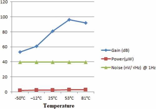
at 200 Hz. Table depicts the comparative analysis of proposed bulk-driven amplifier with previous literature. Table gives the information about variation of different characteristics at different power supply voltages. Table depicts the variation of different characteristics with respect to different temperatures between—50°C to 100°C. Figure shows the characteristics extracted from designed amplifier for different supply voltages. Figure gives the characteristics extracted from designed amplifier for different temperatures.
Table 1. Comparative analysis of proposed bulk-driven amplifier with previous literature
Table 2. Variation of different characteristics at different power supply voltages
Table 3. Variation of different characteristics with respect to different temperatures between—50°C to 100°C
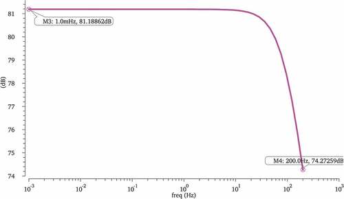
5.2.1. Gain characteristics
Gain of an amplifier can be defined as the difference between input signal and output signal. It is the characteristics which say about to what extent an input signal is amplified at output. It is the ratio of output signal to input signal. The amplifier gain models are depicted in Figures and . The designed BD amplifier using bulk-driven technique has achieved a high gain of value 81 dB, shown in Figure . To examine the reaction of CMRR due to DC offsets, the both inputs terminals are fastened and connected to same input signal, by placing a DC offset voltage as voltage source in between two inputs. The obtained CMRR is calculated manually which is greater than 110 dB.
Figure 9. Biomedical amplifier gain model of input and output signal [NOTE: www.electronics-tutorials.ws/amplifier/amp_1.html]
![Figure 9. Biomedical amplifier gain model of input and output signal [NOTE: www.electronics-tutorials.ws/amplifier/amp_1.html]](/cms/asset/b1a6b523-ba23-408c-8ab9-f47f1e01cb0f/oaen_a_1658966_f0009_oc.jpg)
Figure 10. Ideal amplifier for biomedical signal application [NOTE: www.electronics-tutorials.ws/amplifier/amp_1.html]
![Figure 10. Ideal amplifier for biomedical signal application [NOTE: www.electronics-tutorials.ws/amplifier/amp_1.html]](/cms/asset/3791c2d6-0a32-45c0-bad2-d45e83b69b5b/oaen_a_1658966_f0010_oc.jpg)
Figure 11. Gain characteristics of BD amplifier
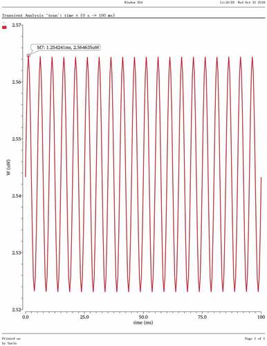
5.2.2. Power characteristics
The interference of device electronics should have very low power dissipation due to increase of harmful heat which has to be less than 1°C because of implanted interference in tissue and tissue vulnerability. And also device should consume low power because the device will be powered by wire or battery, which should have longer battery life and also easily rechargeable at shorter intervals of recharging time. The identification of electrical activity of any biomedical signal requires low power consumption for nano-sized circuits. The power consumption of BD amplifier is 2.5 μW shown in Figure .
Figure 12. Power wave characteristics of BD amplifier
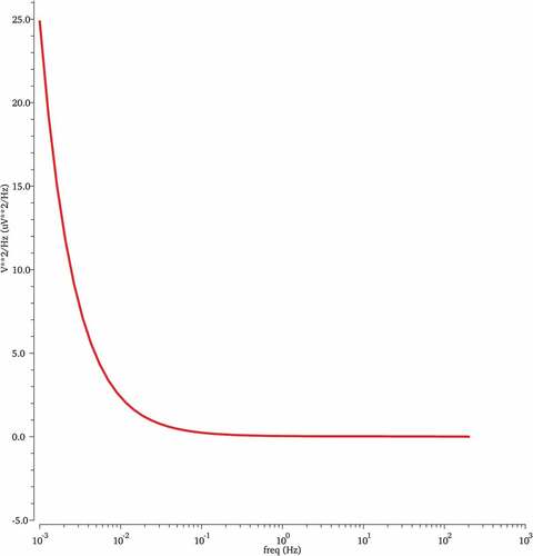
5.2.3. IR noise
In order to design low noise amplifier for biomedical applications, transistor size and biasing are the most important parameters. To estimate the RMS noise of an amplifier, integration of bio-amplifier noise spectral density along with bandwidth is essential. Due to large time constants of integration limits, Rf and Cf in should be considered to be close to zero. The noise displayed at the output of an amplifier is measured as a voltage. The noise is mainly produced by both current and voltage sources. The most widely used specifications for amplifier circuit noise are the IR current and IR voltage noise. These are called IR spectral density function or also called as RMS noise. The V/√Hz is required because of noise power which is added with bandwidth (Hz) or current and voltage noise density will be added with √Hz. The high gain amplifier exhibited only
at 1 Hz and still less noise of
at 200 Hz. Different noise analyses are depicted in Figure , , and . Figure depicts the squared output noise characteristics of bulk-driven gain-boosted amplifier for biomedical applications. Figure depicts the equivalent output noise characteristics of bulk-driven gain-boosted amplifier for biomedical applications.
Figure 13. Noise analysis of BD amplifier
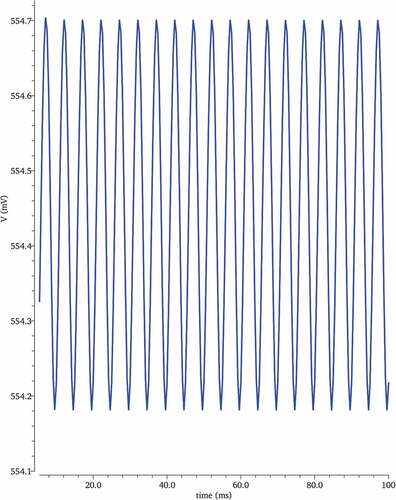
5.2.4. Transient analysis
Transient analysis is usually termed or referred to time domain simulation of the amplifier design which may or may not be in steady state. The transient analysis unlike AC employs the entire large signal model to reckon the circuit behavior. The transient simulation will display: non-linearity, large signal bandwidth, slew limiting, timing issues, etc. The transient analysis is actually the critical simulation test bench for most of the circuit verification. To analyze the transient response of the bio-amplifier, a sine wave of almost 0.01 Hz with 10 mV is applied to the input terminal of proposed amplifier and obtained a magnified 555 mV sinusoidal output signal by using capacitor (C2) that is connected between gain boosting circuit and second stage of design is shown in Figure .
Figure 14. Transient analysis of BD amplifier
5.2.5. Monte Carlo simulation
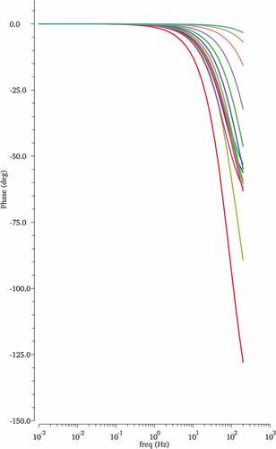
The Monte Carlo simulation method (MCSM) is a statistical method which is used in stochastic simulations along with many applications in areas such as physics, biology, and mathematics. The MCSM is used for a long time to procure numerical approximations of complex functions. This MCSM is typically drawn in engendering observations of some probability distribution and using the obtained sample to approximate the interested function. In this design Monte Carlo parametric simulation is done to evaluate the effect of DC gain, noise, power, transient analysis response, and phase parametric analysis due to mismatches with respect to temperature and capacitance (Figures –, ). Figure depicts the Monte Carlo Simulation of gain characteristics with respect to temperature ranging from −50 to 100°C. Figure depicts the Monte Carlo Simulation of gain characteristics with respect to load capacitances ranging from 1 to1pF. Figure depicts the Monte Carlo Simulation of noise characteristics with respect to temperature ranging from −50 to 100 °C. Figure depicts the Monte Carlo Simulation of noise characteristics load capacitances ranging from 1 fF to 1 pF. Figure depicts the Monte Carlo Simulation of power characteristics with respect to load capacitance ranging from 1 fF to1 pF. Figure depicts the Monte Carlo Simulation of power characteristics with respect to temperature ranging from −50 to100 °C. Figure depicts the Monte Carlo Simulation of transient analysis with respect to load capacitance ranging from 1 fF to 1 pF. Figure depicts the Monte Carlo phase-parametric response with respect to temperature ranging from −50 to 100 °C.
Figure 15. Monte Carlo simulation of gain characteristics with respect to temperature from −50 to100 °C.
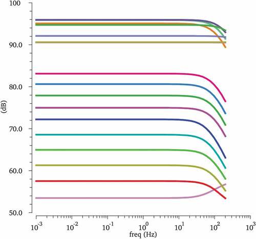
Figure 16. Monte Carlo simulation of gain characteristics with respect to load capacitance from 1 fF to1 pF
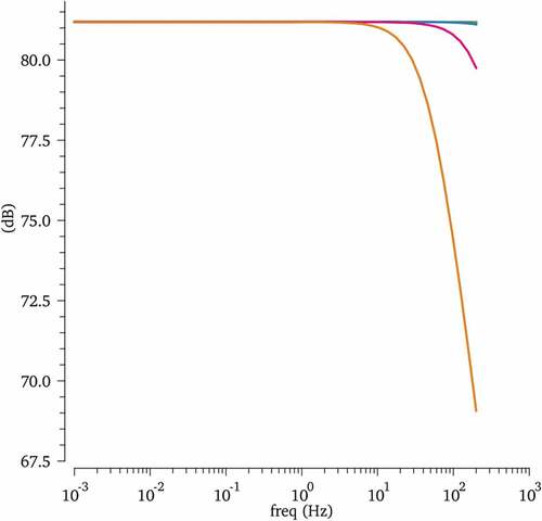
Figure 17. Monte Carlo simulation of noise characteristics with respect to temperature from −50 to100 °C.
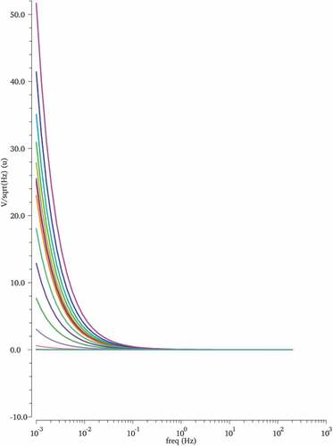
Figure 18. Monte Carlo simulation of noise characteristics with respect to load capacitance from 1 fF to1 pF
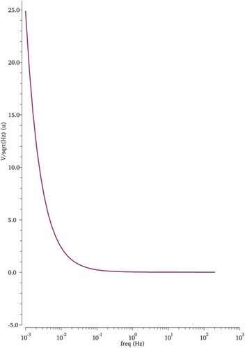
Figure 19. Monte Carlo simulation of power characteristics with respect to load capacitance from 1 fF to1 pF
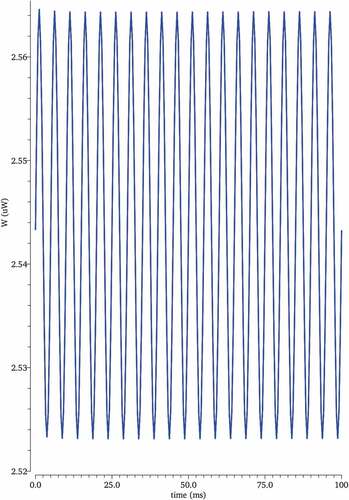
Figure 20. Monte Carlo simulation of power characteristics with respect to temperature from −50 to100 °C.
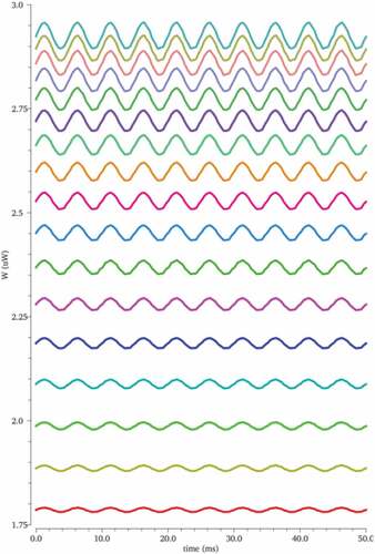
Figure 21. Monte Carlo simulation of transient analysis with respect to load capacitance from 1 fF to1 pF
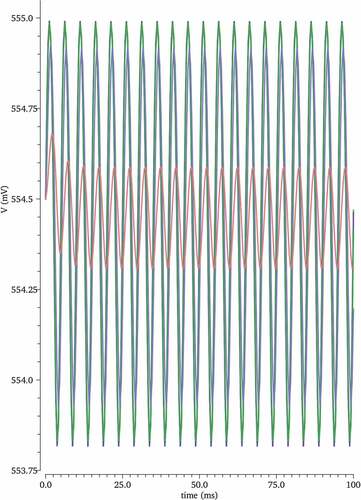
Figure 22. Squared output noise characteristics
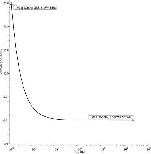
Figure 23. Equivalent output noise characteristics
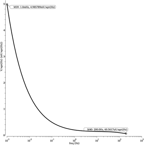
Figure 24. Monte Carlo phase-parametric responses with respect to temperature from −50 to100 °C.
5.2.6. Layout
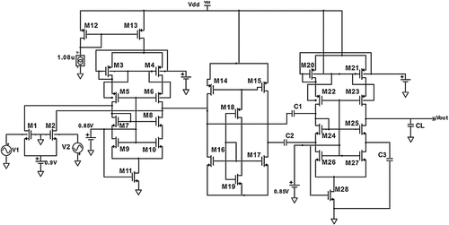
Layout is a three dimensional design of an electronic circuit design with many different elements and interconnections. It is a representation of a circuit design in terms of geometric structures patterned in semiconductor design layers usually referred as topography. The layout of a proposed bulk-driven folded cascode amplifier is designed using Cadence Virtuoso has a dimensions of 17.255 × 35.5 μm (Figure ).
Figure 25. Layout of bulk-driven folded cascode amplifier
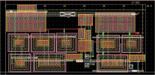
Figure 26. Characteristics extracted from designed amplifier for different supply voltages
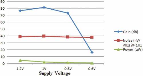
Figure 27. Characteristics extracted from designed amplifier for different temperatures
6. Conclusion
The medical imaging accounts the design and development of electrophysiological monitoring devices to examine the whole human body for proper diagnosis. This article depicts the design of low power and high gain amplifier to amplify the collected vital information from patients using neural recording systems. The proposed research work can also solve and help to ameliorate health coteries and individuals in making a spotlight on innovative and electrifying research area of biomedical electronics. We designed a high gain low noise amplifier for recording the neural signals from human body. This high gain-boosted amplifier can be used in designing and developing neural recording systems like EEG, ECG, ECoG, ENG etc. The smaller size of this proposed amplifier facilitates to develop miniaturized neural systems or biomedical telemetry. In fact, it is going to be the most promising core unit of any neural recording systems or efficient prosthetic wearable devices for electrophysiological signal monitoring because of its efficiency and smaller size. This research work mainly aims to instigate amplifiers which are the core unit to capture electrophysiological signals for all biomedical wearable devices to communicate and to solve set of impediments regarding patient monitoring from advanced health care units in benefit of humanity. A bulk-driven, buffer-biased, gain-boosted amplifier for biomedical signal is designed in 90 nm CMOS technology to capture the activity which consumes low μ power and show cased low noise characteristics. The amplifier achieved 81 dB gain by consuming 2.5 μW power. The IR noise is 39.6 nV/√ Hz for BD FC-OTA at 1 Hz. The layout of a proposed bulk-driven folded cascode amplifier is designed using Cadence Virtuoso has a dimensions of 17.255 × 35.5 μm. The designed FC-OTA can be best suitable for biomedical signal recording applications.
Conflicts of Interest
The authors declare no conflict of interest.
Acknowledgements
We feel obliged to take this opportunity to thank Centre for Excellence in VLSI and Nano Electronics, Karunya Institute of Technology and Sciences (Deemed University), Coimbatore and CDAC, Hyderabad for taking keen interest and providing base, encouragement to our research work.
Additional information
Funding
Notes on contributors
Sarin Vijay Mythry
Sarin Vijay Mythry was born in Sangareddy in Telangana State, India. He received Master in Engineering Degree in VLSI Design from Karunya University, Coimbatore in 2009, Bachelor Degree in Electrical Engineering from JNTU, Hyderabad, Telangana State, India. Now he is working as research scholar towards his Ph.D. Degree in Electronics Engineering with specialization in Low power Biomedical VLSI technology at Karunya University. His interests are in Micro Electronic System Design using CMOS Technology, Biomedical VLSI, RF Design and Bio-Electronics Engineering.
D. Jackuline Moni
Dr. D. Jackuline Moni working as a Professor in ECE Department, Karunya University. She is in charge of M.Tech (VLSI Design) in Karunya university. She did her B.Tech in Electronics Engineering at Madras Institute of Technology, Anna University, M.E in (Applied Electronics) from Government College of Technology, Coimbatore, and her Ph.D in (VLSI DESIGN) from Anna University, Chennai. She has over 25 years of teaching experience .She has guided more than 70 UG and PG projects in the area of VLSI design and Embedded systems. She has presented and published more than 60 papers in National and International Journals and conferences. Her areas of interest are CAD VLSI Design, Device modeling, Low Power VLSI Design, analog VLSI and Embedded System Design.
Related Research Data
References
- Agrawal, G., & Sankaran, A. (2017). A modified bias scheme for highgain low-noise folded cascode OTAs International Conference on Electron Devices and Solid-State Circuits (EDSSC), 2017 International Conference on Electron Devices and Solid-State Circuits (EDSSC). IEEE. INSPEC Accession Number: 17413811. doi:ISOCC.2016.7799786/EDSSC.2017.8126531
- Bano, S., Narejo, G. B., Shah, A., & Syed, M. U. (2018). Power efficient fully differential bulk driven OTA for portable biomedical application. Electronics, 7(3), 41. doi:10.3390/electronics7030041
- Blalock, B. J., Allen, P. E., & Rincon-Mora, G. A. (1998). Designing 1-V Op Amps using standard digital CMOS technology. IEEE Transactions on Circuits and Systems II Analog and Digital Signal Processing, 45(7), 769–27. doi:10.1109/82.700924
- Carrillo, J. M., Torelli, G., P-Aloe, R., Valverde, J. M., & D-Carrillo, J. F. (2010). Single-pair bulk driven CMOS input stage: A compact low-voltage analog cell for scaled technologies. Integration of VLSI Journal, 43, 251–257. doi:10.1016/j.vlsi.2010.03.002
- Carvajal, R. G., R-Angulo, J., L-Martin, A. J., Torralba, A., Galan, J. A. G., Carlosena, A., & Chavero, F. M. (2005). The flipped voltage follower: A useful cell for low voltage low power circuit design. IEEE Transactions on Circuits and Systems I, 52, 1276–1291. doi:10.1109/TCSI.2005.851387
- Cotrim, E. D. C., & Ferreira, L. H. C. (2012). An ultra-low-power CMOS symmetrical OTA for low-frequency Gm-C applications. Analog Integrated Circuits and Signal Processing, 71, 275–282. doi:10.1007/s10470-011-9618-5
- El Mourabit, A., Lu, G., & Pittet, P. (2005). Wide linear range sub-threshold OTA for low power, low voltage and low frequency applications. IEEE Transactions on Circuits and Systems I, 52, 1481–1488. doi:10.1109/TCSI.2005.852011
- Ferreira, L. H. C., Pimenta, T. C., & Moreno, R. L. (2007). An ultra–low-voltage ultra-low power MOS miller OTA with rail-to-rail input/output swing. IEEE Transactions on Circuits and Systems II: Express Briefs, 54, 843–847. doi:10.1109/TCSII.2007.902216
- Guzinski, A., Bialko, M., & Matheau, J. C. (1987). Body-driven differential amplifier for application in continuous-time active C-filter. Proceedings of ECCD, 315–319.
- Hariprasad, C., & Dejan., M. (2017). A high dynamic-range neural recording chopper amplifier for simultaneous neural recording and stimulation. IEEE Journal of Solid-state Circuits, 1–12. doi:10.1109/JSSC.2016.2645611
- Karimi-Bidhendi, A., Malekzadeh-Arasteh, O., Lee, M.-C., McCrimmon, C. M., Wang, P. T., Mahajan, A., … Heydari, P. (2017). CMOS ultralow power brain signal acquisition front-ends: Design and human testing. IEEE Transactions on Biomedical Circuits and Systems, 11(5), 1111–1122. doi:10.1109/TBCAS.2017.2723607
- Khateb, F., Biolek, D., Khatib, N., & Vávra, J. (2010). Utilizing the bulk-driven technique in analog circuit design. Proceedings of the IEEE 13th International Symposium on Design and Diagnostics of Electronic Circuits and Systems (DDECS), Vienna, Austria.
- Kim, D., Kim, B., & Nam, S. (2015). A transconductor and tunable Gm-C high-pass filter linearization technique using feed forward Gm cancellation. IEEE Transactions on Circuits and Systems II: Express Briefs, 62, 1058–1062. doi:10.1109/TCSII.2015.2456611
- Kim, H., & Cha, H.-K. (2018b, August). An ultra-low power low noise neural recording analog front-end IC for implantable devices. Journal of Semiconductor Technology and Science, 18(4), doi:10.5573/JSTS.2018.18.4.454
- Kim, H. S., & Cha, H. K. (2018a). A low-noise biopotential CMOS amplifier IC using low power two stage OTA for neural recording applications. Journal of Circuits, Systems and Computers, 27(05), 1850068. doi:10.1142/S0218126618500688
- Kim, H. S., & Hyouk-Kyu., C. (2016). A low-power, low-noise neural recording amplifier for implantable biomedical devices. 2016 International SoC Design Conference (ISOCC), Jeju, South Korea. 275–276. IEEE. INSPEC Accession Number: 16560669, doi:10.1109/ISOCC.2016.7799786.
- Lee, C.-J., & Song, J.-I. (2019). A chopper stabilized current feedback instrumentation amplifier for EEG acquisition applications. Vol.7 IEEE ACCESS January, 2019.
- Lee, S.-Y., & Cheng, C.-J. (2009). Systematic design and modeling of OTA-C filter for portable ECG detection. IEEE Transactions on Biomedical Circuits and Systems, 3, 53–64. doi:10.1109/TBCAS.2008.2007423
- Lo, T.-Y., & Hung, C. C. (2007). A 1-V 50 MHz pseudo differential OTA with compensation of mobility reduction. IEEE Transactions on Circuits and Systems II, 54, 1047–1051. doi:10.1109/TCSII.2007.907559
- Moreno, R. F. L., Baruqui, F. A. P., & Petraglia, A. (2015). Bulk-tuned Gm-C filter using current cancellation. Microelectronics, 46, 777–782. doi:10.1016/j.mejo.2015.05.010
- Moulahcene, F., Bouguechal, N.-E., Benacer, I., & Hanfoug, S. (2014). Design of CMOS two-stage operational amplifier for ECG monitoring system using 90nm technology. International Journal of Bio-Science and Bio-Technology, 6, 55–66. doi:10.14257/ijbsbt.2014.6.5.07
- Mythry, S. V., & Moni, D. J. (2018). 21nV/vHz 73 dB folded cascode OTA for electroencephalograph activity. Springer Soft Computing Systems,ICSCS. doi:10.1007/978-981-13-1936-5_44
- Pulido, R., Santana-Abril, J., Sosa, J., & Montiel-Nelson, J. (2017). A 1.2-V 730-nW 10-Hz-3.5-kHz programmable biopotential front-end. Midwest Symposium on Circuits and Systems. ISSN: 1565–1568. doi:10.1109/MWSCAS.2017.8053235
- Raikos, G., & Vlassis, S. (2010). 0.8 V bulk-driven operational amplifier. Analog IntegrCirc Sig Process (springer), 63, 425–432. doi:10.1007/s10470-009-9425-4
- Raj, N., Sharma, R. K., Jasuja, A., & Gard, R. (2010). A low power OTA for biomedical applications. Cyber Journals: Multidisciplinary Journals in Science and Technology. Journal of Selected Areas in Bioengineering (JSAB). December Edition.
- Razaei, F., & Azhari, S. J. (2015). Transconductor linearization based on adaptive biasing of source degenerative MOS transistors. Circuits, Systems and Signal Processing, 34, 1149–1165. doi:10.1007/s00034-014-9902-6
- Rodriguez-Villegas, E., Yufera, Y., & Reuda, A. (2004). A 1.25V micropower Gm-C filter based on FGMOS transistor operating in weak inversion. IEEE Journal of Solid-State Circuits, 39, 100–111. doi:10.1109/JSSC.2003.820848
- Sadock, B. J., Sadock V. A. Kaplan and Sadock’s comprehensive textbook of psychiatry (Vol. 1, 10 ed.). Wolters Klumers. https://www.electronics-tutorials.ws/amplifier/amp_1.html
- SamadSheikhaei, M. G. (2019). A low power low noise CMOS bio-potential amplifier for multi-channel neural recording with active DC-rejection and current sharing. Elsevier Microelectronics Journal 83 (2019): 197–211.
- Sarin Vijay, M. D., & Moni, J. (2018). High gain low noise bulk driven folded cascode OTA for electroencephalograph activity. International Journal of Pure and Applied Mathematics, 120(6), 8065–8088.
- Sharan, T., & Bhadauria, V. (2016). Sub-threshold, cascode compensated, bulk driven OTAs with enhanced gain and phase margin. Microelectronics Journal, 54, 150–165. doi:10.1016/j.mejo.2016.05.009
- Sharan, T., & Bhadauria, V. (2017). Fully differential, bulk driven, class AB, sub-threshold OTA with enhanced slew rates and gain. Journal of Circuits, Systems, and Computers, 26, 1750001. doi:10.1142/S0218126617500013
- Sharan, T., Chetri, P., & Bhadauria, V. (2018). Ultra-low-power bulk-driven fully differential subthreshold OTAs with partial positive feedback for Gm-C filters. Analog Integrated Circuits and Systems, 94, 427–447. doi:10.1007/s10470-017-1065-5
- Szczepanski, S., Pankiewicz, B., Koziel, S., & Wojcikowski, M. (2015). Multiple output differential OTA with linearized bulk driven active-error feedback loop for continuous time filter applications. International Journal of Circuit Theory and Applications, 43, 1671–1686. doi:10.1002/cta.2034
- Worapishet, A., & Naphaphan, C. (2003). Current feedback source degenerated CMOS transconductor with very high linearity. Electronic Letter, 39, 17–18. doi:10.1049/el:20030050
- Yang, T., & Holleman, J. (2015). An ultralow-power low-noise CMOS biopotential amplifier for neural recording. Circuits and Systems II: Express Briefs, IEEE Transactions On, 62, 927–931. doi:10.1109/TCSII.2015.2457811
- Zarifi, M. H., Frounchi, J. A., Tinati, M., Farshchi, S., & Judy, J. (2010). A low-noise low-power front-end amplifier for neural-recording applications. Biomedical Engineering: Applications, Basis and Communications, 22, 301–306.
- Zhang, J., Chan, S.-C., & Lei., W. (2014). A 1.8 µW area-efficient bio-potential amplifier with 90 dB DC offset suppression. Midwest Symposium on Circuits and Systems (p. 286–289), The IEEE 57th International Midwest Symposium on Circuits and Systems (MWSCAS), College Station, Texas, USA. doi:10.1109/MWSCAS.2014.6908408.
- Zuo, L., & Islam, S. K. (2013). Low-voltage bulk-driven operational amplifier with improved transconductance. IEEE Transactions on Circuits and Systems I: Regular Papers, 60(8), 2084–2091. doi:10.1109/TCSI.2013.2239161
- Zuo, L., & Syed, K. I. (2013). Low- voltage bulk-driven operational amplifier with improved transconductance. IEEE Transactions on Circuits and Systems I: Regular Papers. doi:10.1109/TCSI.2013.2239161