
Abstract
Aluminium (Al) thin films (thickness ranging between 500 and 600 nm) were deposited on stainless-steel substrates at varying radio-frequency (RF) power by magnetron sputtering at a constant substrate temperature of 90°C. Characterisations were undertaken by field emission scanning electron microscopy (FESEM), optical surface profilometry (OSP), atomic force microscopy (AFM), X-ray diffraction (XRD), selected Fourier-transform infrared spectroscopy (FTIR), nanoindentation, and micro-scratch tests. At high RF powers (300–350 W), there was the formation of less porous, dense, and continuous Al thin films with better resistance to scratch failure. The high roughness on films deposited at 200 and 250 W was due to high porosity and oxides observed on the FESEM micrographs.
PUBLIC INTEREST STATEMENT
Aluminum thin films find applications in various fields including optics where they are used as coatings on aspheric mirrors. In such cases, these coatings are exposed to abrasive loading especially during cleaning and normal operating conditions. For example, during the cleaning of a car, the surfaces of the mirrors are scratched by abrasive cloth to remove the dirt. If the thin film coating on the mirrors is not resistant to the loading, the film is likely to degrade and lower the performance of the mirrors. As such, their wear behavior, known as scratch characteristics, is very important. This paper illustrates the wear characteristics of Al thin films under micro-wear loads. The relationship between the deposition conditions of the Al thin films and wear behavior is reported in the paper. The conditions for producing the best Al thin films for wear resistance are described.
1. Introduction
Aluminium thin films are widely used in microelectronic devices as interconnects for semiconductor chips because of their low resistivity (Quintana et al., Citation1999). Because of their high optical reflectance, aluminium thin films have also been used in solar applications such as in solar cookers (Lugolole & Obwoya, Citation2015) and solar concentrators (Muralidhar Singh et al., Citation2018). The high optical reflectance also makes them be used as coatings in space and aspheric mirrors (Barron, Citation2005). Aluminium films are also used as anticorrosive coatings of substrates such as steels in mediums such as sea (Chaliampalias et al., Citation2008), industrially polluted medium (Lee et al., Citation2016) and so forth. Their application as anticorrosive coatings is enhanced by their sacrificial behaviour in high-chloride containing media in which they react with the electrolyte to form impervious and inert compounds to protect the substrate (Mwema, Oladijo, Akinlabi et al., Citation2018).
Regardless of the application, the properties of aluminium thin films depend on the process parameters, type and properties of the substrate (Mwema, Oladijo, Akinlabi et al., Citation2018). Various studies have been undertaken to evaluate the effect of different factors on properties of aluminium thin films (Her & Wang, Citation2015; Kao & Lin, Citation2012; Mwema, Oladijo, Akinlabi et al., Citation2018, Citation2018; Mwema, Oladijo, Sathiaraj et al., Citation2018; Martin et al., Citation1995; Pakhuruddin et al., Citation2012; Qiu et al., Citation2002). The effect of the type of substrate on the structural evolution of Al thin films has been reported recently (Khachatryan et al., Citation2018) and shown that larger and well-defined grain sizes are formed when deposited on metallic substrates. Sputtering is one of the attractive techniques of preparing aluminium thin films (D’Heurle, Citation1970) and it is controlled by various process parameters including temperature, power, argon gas flowrate, bias voltage, etc. (Simon, Citation2018; Wasa & Hayakawa, Citation1992). Of the existing literature, the influence of sputtering power on properties of aluminium thin films is not extensively reported. To fill this gap, therefore, the aim of this work is to study the microstructure and mechanical behaviour of aluminium thin films deposited at varying radio-frequency (RF) sputtering power.
2. Experimental
Aluminium thin films were deposited on stainless steel substrates using RF magnetron sputtering process (Mwema, Oladijo, Akinlabi et al., Citation2018; Mwema, Oladijo, Sathiaraj et al., Citation2018). The wt. % main constituents of the substrates were 0.021 C, 0.809 Mn, 16.86 Cr, 1.920 Mo, 9.985 Ni, 0.293 Cu and 68.98 Fe. The substrates dimensions were 50 mm by 50 mm and thickness of 2 mm. Deposition of Al thin films on metals such as stainless steel is important for applications as metal-barrier for semi-conductors. Before sputtering, the substrates were ground with SiC grades (#200-#1200), then cleaned with deionized water, rinsed in acetone and dried in high-pressure hot air. Pure Al (99.99%) was used as a target and it was mounted at 130 mm apart from the rotating substrate holder (the holder rotates at 5 rpm). The deposition chamber was kept at a vacuum pressure of 1 × 10⁻⁵ mbar throughout the deposition process. Prior to deposition, the substrate was pre-sputtered for 30 minutes to remove any oxides on the surface. The sputtering was then undertaken for various RF powers (150, 200, 250, 300 and 350 W) at a constant substrate temperature of 90°C for 2 hours using HHV auto 500 sputtering system. The sputtering was undertaken under inert conditions of argon gas at a constant flowrate of 10 sccm. The samples were then left to cool under vacuum for 3 hours after which they were removed and sliced into 10 mm by 10 mm pieces for characterization.
The SEM imaging was undertaken using Carl Zeiss-SUPRA40 FE-SEM at the top surface of the samples. The topography measurement of the films was undertaken using atomic force microscopy (AFM) Veeco Dimension 3100. The procedure of AFM imaging used here has been described in our previous publications (Mwema, Oladijo, Akinlabi et al., Citation2018; Mwema, Oladijo, Sathiaraj et al., Citation2018). For each AFM, five images were taken at different regions of the surface. The nanoindentation measurements were undertaken using TI950 TriboIndenterTM nanomechanical (Hysitron, Inc., USA) facility at a maximum load of 250 μN and a loading time of 15 seconds. From the nanoindentation results, the hardness and elastic modulus were determined as described in the literature (Mwema, Akinlabi et al., Citation2018). The crystalline characteristics of the Al thin films were studied via XRD method using Bruker D8 Advance diffractometer. The intensity curves were obtained in the 2θ range between 10° and 100° using CuKα radiation. The FTIR spectra of some selected Al films were undertaken at a resolution of 4 cm−1 and 64 scans for each spectrum within the absorption band range of 400–4000 cm−1. Micro-scratch analyses were undertaken using Anton Paar (formerly CSM instruments, Graz Austria) under a progressive loading (30 mN-1500 mN). The equipment has a friction table with a minimum loading of 30 mN and a panorama camera which allows for in-situ and ex-situ examination of the surface failure occurring during scratching. The equipment uses a Rockwell, L-172 diamond scratch tool of radius 100 μm. The scratch tests were undertaken at a constant loading rate of 1940 mN/min.
3. Results and discussion
3.1. FESEM microstructure and surface roughness
The surface morphologies of the thin aluminium films sputtered on stainless steel at different RF powers and constant temperature of 90°C are shown in Figure . Generally, the morphologies are characterised by oxides, porosity and rough structures. At RF powers of 150–250 W, the films were discontinuous with most of its structure having oxides and regions of exposed surfaces of the substrate. More conspicuous at 250 W, the surface is composed of very rough and highly oxidized surfaces, making the surface appears granulate. At 300 W and 350 W, the microstructures appear denser and continuous with few oxides. It can also be seen that most of the surface of the substrate are fully covered by the films. At 350 W, there are occasionally large structures on the surface of the Al thin films, which implies nucleation and growth of Al during sputtering at this power. Table shows the values of root-mean-square roughness obtained through the optical surface profiling (OSP) and atomic force microscope (AFM). These results suggest that higher sputtering power leads to the formation of a dense and smooth microstructure of Al thin films on stainless steel substrates.
Figure 1. Field emission scanning electron microscope (FESEM) micrographs of aluminium films sputtered on stainless-steel substrates at varying power. The FESEM images were taken at magnifications of X50,000
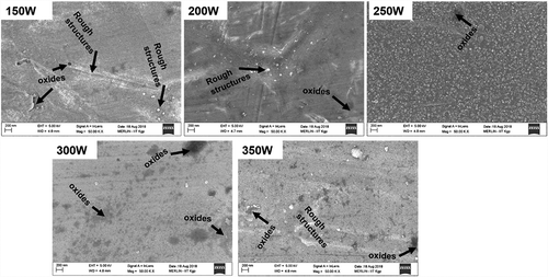
Table 1. Roughness values of thin aluminium films sputtered on stainless-steel substrates at different rf powers. The roughness values were determined by the optical surface profilometer (OSP) and AFM measurements
3.2. Atomic force microscopy (AFM) characterisation
The surface topography was characterized by AFM observations, AFM height distribution histograms and bearing ratio curves. The typical AFM topographical micrographs of Al thin films RF sputtered on steel substrates are represented in Figure . The general observation is that as the power increases, the structure of the Al films develops and becomes less amorphous (distinct). At 350 W, the grains of the Al films can be clearly observed in the 3D view (Figure ) of the AFM images. On the contrary, the structures appear amorphous and irregular at low RF sputtering power. Similar results relating to RF power and surface topography has been reported at high powers (Kumar & Rao, Citation2012). Formation of dense and continuous microstructure and topography films at high RF power can be attributed to the fact that high power increases the energy of the argon gas in the plasma such that the kinetic energy of the dislodged atoms from the target (aluminium in this case) is increased. Atoms hitting the substrate at high kinetic energy diffuse more on the substrate surface to form dense, continuous and less amorphous films rather than amorphous as it is observed at low RF powers (Ahmadipour et al., Citation2017).
Figure 2. Representative AFM micrographs of the aluminium films sputtered at different powers. Colour intensity bars are shown on the righthand of each micrograph. The AFM measurement parameters are also indicated
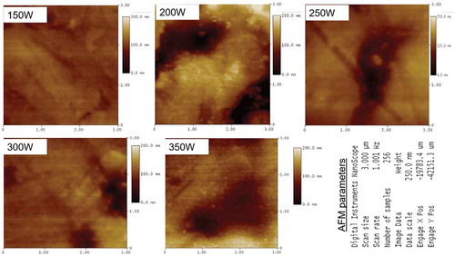
Figure 3. Characteristics 3D AFM images illustrating the porosity and developed surface structures of Al film RF sputtered at 250 W 350 W, respectively
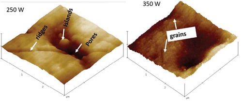
The AFM roughness characteristics (statistical) computed according to ISO standard 25,178–2:2012 are shown in Table (Mwema, Oladijo, Sathiaraj et al., Citation2018). The films prepared at 250 W have the highest roughness values and this can be attributed to the island and porosity extensively observed on FESEM micrographs (Figure ) and 3D AFM image (Figure ). The lowest roughness obtained at 150 W is an indication of lower structural growth at low RF sputtering power. The roughness skewness (Rsk) values for all the surfaces are negative, which indicate a good load-bearing capacity for the films and that valleys are dominant structures for all the films. The very high negative value obtained at 250 W is an indication of the existence of high degree of porosity. The roughness kurtosis (Rku) values were all higher than 3, except for surfaces at 350 W, indicating that the surfaces exhibited spiky structures. The Rku value at 350 W (less than 3) indicate bumpy surfaces with very high peaks and low valleys, which can be attributed to the well-defined grain and dense (less amorphous) structures shown in Figure .
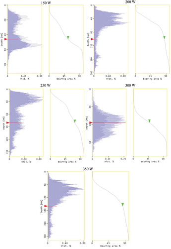
Figure shows the height distribution histograms and the bearing ratio of the RF sputtered Al films at various powers. The height histograms are used to illustrate the nature and distribution of the structures at the surfaces of the films. The distribution of height structures of most engineering surfaces can be estimated by Gaussian distribution which is defined by the ratio Rq/Ra (Rajesh Kumar & Subba Rao, Citation2012). The percentage (%) bearing areas on the histograms were computed using the Nanoscope software available on the AFM facility. Surfaces are said to be Gaussian if this ratio is 1.25 and as seen in Table the values are generally close to this theoretical value indicating that at the imaging scale the surfaces can be approximated by the Gaussian distribution and the statistical relationships for Ra, Rq, Rsk and Rku can be applied in this analysis. As seen in Figure , all the films exhibit noncontinuous histograms (with peaks) indicating a high degree of roughness due to unpolished substrates. These peaks are more pronounced across the histograms for films deposited at 200 and 250 W which can be attributed to the high degree of porosity and islands described through FESEM microscopy. The bearing ratio describes how the occurrence of solid material depends on the height of the surface features. The bearing curves in Figure indicate that the bearing ratios are zero below depths of 5, 4, 3, 10 and 6 nm for 150, 200, 250, 300 and 350 W, respectively, which implies that the surface structures are connected to each other at these heights above the surface of the Al thin films.
Figure 4. Height distribution histograms and bearing ratio for Al thin films RF sputtered at different powers
3.3. Nano-hardness
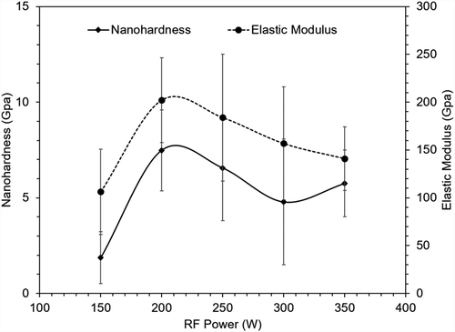
Figure shows the values of nano-hardness and elastic modulus of the films deposited at different sputtering powers. As seen, the microhardness increased from 1.9 to 7.5 GPa and then decreased gradually with increasing RF power. The elastic modulus exhibited a similar relationship with the RF power. The highest mechanical properties (hardness and elastic modulus) were obtained at 200 and 250 W, beyond which the hardness and elastic modulus can be seen to decrease. However, as it will be seen on the scratch test, samples with lower hardness and elastic modulus exhibited higher deformation resistance which can be probably due to denser and continuous films formed at those powers as compared to films at lower powers which exhibited high oxidation and porosity as discussed in the FESEM observations.
Figure 5. Nanohardness and reduced elastic modulus of Al thin films deposited on stainless steel substrates at different sputtering powers
3.4. X-ray diffraction (XRD)
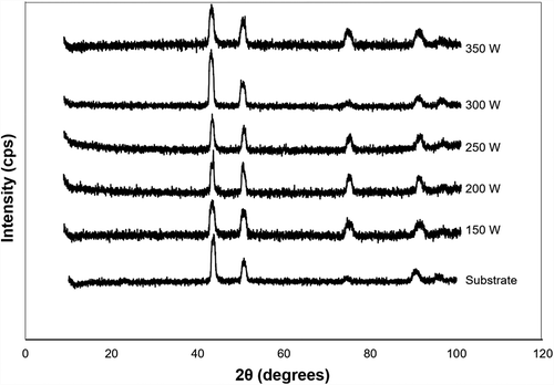
Figure shows the XRD spectrum of Al thin films deposited at different RF powers taken on three surfaces for each parameter. The XRD for the substrate is also included for comparison. As seen, the profiles revealed nearly the same XRD patterns for all the RF sputtering powers. The peaks obtained at 42°, 50° and 90° are obvious characteristics of the stainless-steel substrates’ planes. There are no other obvious diffraction peaks characteristic of aluminium thin films, except minor changes observed in the spectrum as the RF power increases. At 75° and 90°, the intensity of the peaks tends to increase on the Al deposited substrates, which could be a minor effect of the deposition. Usually, crystalline Al thin films would be detected between 38° and 39°. These results indicate that the Al thin films obtained in this work are amorphous. The stability of the amorphous structure of Al thin films is not affected by varying the RF power from 150 W to 350 W at a constant substrate temperature of 90°C.
Figure 6. X-ray diffraction (XRD) patterns of Al thin films sputtered at different RF power
3.5. Fourier-transform infrared spectroscopy (FTIR)
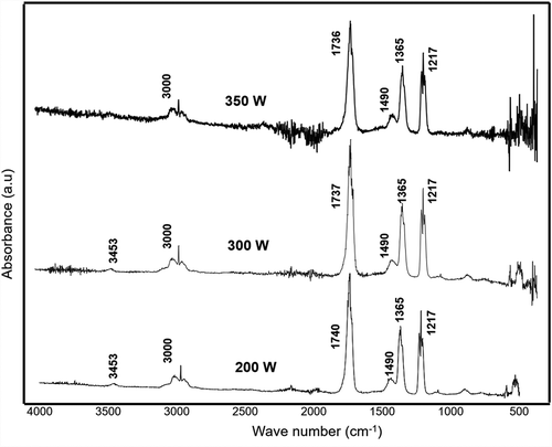
Figure shows the typical FTIR spectra of unpolished 316 L stainless steel substrates coated with thin aluminium films prepared at 200 W, 300 W and 350 W. The fundamental vibrations of the compounds are concentrated in the finger print region of the infrared spectrum for the three samples. The few and small absorption bands observed, in samples prepared at 200 and 300 W, in the range of 3000–4000 cm−1 are assigned to pseudo-boehmite and bayerite products resulting from the contamination of the unpolished substrate and oxidation. However, these bands are not observable in the samples prepared at 350 W. This could be attributed to the SEM observations that most of the substrate surface was fully covered by the Al films due to the high sputtering yield expected at higher power (Ahmadipour et al., Citation2017). The narrow bands between 500 and 2000 cm−1 can be attributed to the stretching vibration mode of Al-O and C-O.
Figure 7. FTIR of thin aluminium films deposited on stainless-steel substrates at rf powers of 200, 300 and 350 W
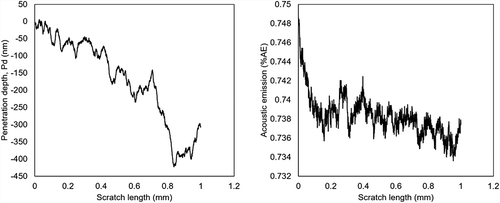
3.6. Micro-scratch analysis
Figure shows the panorama views of the scratch tracks obtained during the scratch test of all the surfaces according to ASTM G171-03(2017). The scratch tracks are clearly observable in all the surfaces indicating the occurrence of wear of aluminium films at these load range (30–1500 mN). Figures –1 show the tribological characteristics as functions of the distance of scratch and as shown, the penetration depths (Pd) of the tool and acoustic emissions (%AE) are considerably dependent on the sputtering power. The maximum Pd was obtained as 380, 680, 520, 420 and 425 nm for films sputtered at 150, 200, 250, 300 and 350 W, respectively. These results indicate that the Al films deposited at 200 and 250 W were fully delaminated from the substrate after 1000 μm scratch length. The results can be attributed to the porosity and oxides on FESEM and higher presence of Al-O groups as shown by the FTIR analyses. For films at 200 and 250 W, the penetration depth increases linearly across the scratch length whereas the in the other films, the Pd profiles exhibit a roughly indentation profile. In some instances, the depth decreases and then continues to increase. The decrease in depth is probably associated with the plastic collapse of the film around the porous regions. From these results, the maximum scratch depth initially increases and then decreases with the increasing sputtering power indicating a strong dependence of scratch failure on RF power. The acoustic emissions (%AE) for all the surfaces are characterised by very high noise, which indicate the random breakdown of the films throughout the scratch distance. These observations are further attributed to amorphous, porous and oxidised surfaces of the films as shown by the FESEM, AFM and XRD characterisations. The scratching process, in this case, can be said to “close-up” the oxides and pore regions of the films in cases where the tip does not penetrate the substrate (at 300 and 350 W).
Figure 8. Panorama images of the Scratch tracks during scratch testing of various Al films RF sputtered at different powers
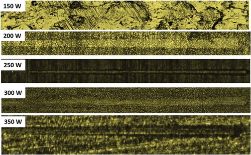
Figure 9. Scratch test: The depth of penetration (Pd) and acoustic emission (AE) for films deposited at 150 W
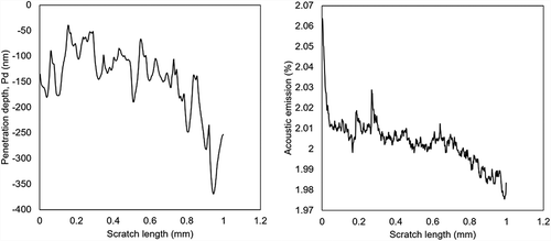
Figure 10. Scratch test: The depth of penetration (Pd) and acoustic emission (AE) for films deposited at 200 W
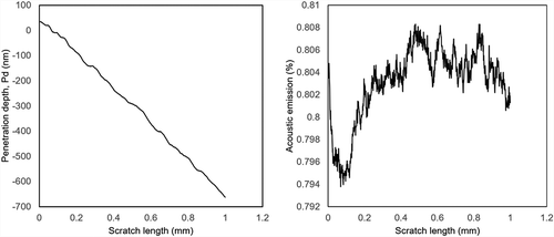
Figure 11. Scratch test: The depth of penetration (Pd) and acoustic emission (AE) or films deposited at 250 W
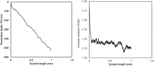
Figure 12. Scratch test: The depth of penetration (Pd) and acoustic emission (AE) for films deposited at 300 W
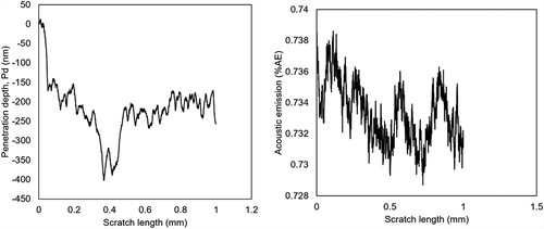
Figure 13. Scratch test: The depth of penetration (Pd) and acoustic emission (AE) or films deposited at 350 W
4. Summary and conclusions
Increase in RF sputtering power (150–350 W) results in the formation of denser, continuous and less amorphous aluminium thin films although the trend is not linear as extensively reported in the literature. The trend briefly changes after 250 W, which implies that optimisation is necessary with other combinations of parameters. The microstructure of films deposited at 200–250 W were characterised by high oxides, porosity and roughness whereas those deposited at 300–350 W were smoother with less porosity and oxidation. Higher values of nano-hardness and elastic modulus were obtained at films deposited at 200–250 W. At 300–350 W, the films exhibited lower hardness and elastic modulus properties. The progressive loading micro-scratch analysis revealed that the films exhibiting high roughness, porosity, oxides and discontinuous topography (200–250 W) are prone to scratch failure based on the depth of penetration (Pd) measurements of the scratch tool.
Major conclusions
The films deposited at 200 and 250 W exhibited porous and oxidized microstructures and high hardness and elastic modulus.
The films deposited at 300-350 W were continuous and with dense microstructural features. They had lower hardness and elastic modulus.
The films deposited at 300-350 W exhibited higher resistance to scratch tool penetration that 200-250 W films. These results indicate that scratch failure is significantly influenced by the presence of porosity and oxides.
As such, to achieve high scratch resistance Al thin films, porosity and oxidation should be reduced.
Acknowledgements
The GES 4.0 postdoctoral fellowship (2019/2020) of the University of Johannesburg is highly acknowledged. The authors further thank Prof. JD Majumdar of IIT Kharagpur, for hosting the researcher during characterisation of the films and organising for access to the CRF laboratories (FESEM and nanoindentation). Prof. TS Sathiaraj of Botswana International University of Science & Technology (BIUST) is highly acknowledged for allowing us to use their sputtering facility.
Additional information
Funding
Notes on contributors

F. M. Mwema
Dr. F. M. Mwema is a postdoctoral researcher and a lecturer at the University of Johannesburg, South Africa and Dedan Kimathi University of Technology, Kenya respectively. He obtained BSc and MSc degrees in mechanical Engineering from Jomo Kenyatta University of Agriculture & Technology, Kenya in 2011 and 2015 respectively. He has a Ph.D. in Mechanical Engineering from the University of Johannesburg, which he obtained in 2019. His Ph.D. research work involved thin film coatings for surface protection and functional components. He has interests in advanced manufacturing, severe plastic deformation processes, additive manufacturing, thin film depositions, surface engineering, and materials characterizations. In thin films, Dr. Mwema has interest in fractal theory of coatings for enhanced depositions and behavior in advanced applications. He has published more than 50 articles in peer-reviewed journals, conferences and book chapters. He supervises and mentors several students, currently with 4 masters and 3 Ph.D. students. He has over six years of teaching and training in mechanical engineering.
References
- Ahmadipour, M., Ayub, S. N., Ain, M. F., & Ahmad, Z. A. (2017). Structural, surface morphology and optical properties of sputter-coated CaCu3Ti4O12thin film: Influence of RF magnetron sputtering power. Materials Science in Semiconductor Processing, 66(March), 157–12. https://doi.org/10.1016/j.mssp.2017.04.019
- Barron, L. W. (2005). High-reflectance, sputter-deposited aluminum alloy thin films for micro-electro-mechanical systems. Rochester Institute of Technology
- Chaliampalias, D., Vourlias, G., Pavlidou, E., Stergioudis, G., Skolianos, S., & Chrissafis, K. (2008). High temperature oxidation and corrosion in marine environments of thermal spray deposited coatings. Applied Surface Science, 255(5 Part 2), 3104–3111. https://doi.org/10.1016/j.apsusc.2008.08.101
- D’Heurle, F. M. (1970). Aluminum films deposited by rf sputtering. Metallurgical and Materials Transactions B, 1(3), 725–732. https://doi.org/10.1007/BF02811600
- Her, S., & Wang, Y. (2015). Temperature effect on microstructure and mechanical properties of aluminum film deposited on glass substrates. 22(June), 268–272. Indian Journal of Engineering & Materials Sciences. https://doi.org/10.1166/asl.2013.5005
- Kao, M. T., & Lin, J. F. (2012). Effects of deposition conditions of the Al film in Al/glass specimens and annealing conditions on internal stresses and hillock formations. Thin Solid Films, 520(16), 5353–5360. https://doi.org/10.1016/j.tsf.2011.12.027
- Khachatryan, H., Lee, S., Kim, K.-B., Kim, H.-K., & Kim, M. (2018, November). Al thin film: The effect of substrate type on Al film formation and morphology. Journal of Physics and Chemistry of Solids, 122(May), 109–117. https://doi.org/10.1016/j.jpcs.2018.06.018
- Kumar, B. R., & Rao, T. S. (2012). Influence of sputtering power on physical properties of nanostructured zinc aluminum oxide thin films for photovoltaic applications. Digest Journal of Nanomaterials and Biostructures, 7(3), 1051–1061.
- Lee, H.-S., Singh, J., Ismail, M., & Bhattacharya, C. (2016). Corrosion resistance properties of aluminum coating applied by arc thermal metal spray in SAE J2334 solution with exposure periods. Metals (Basel), 6(3), 55. https://doi.org/10.3390/met6030055
- Lugolole, R., & Obwoya, S. K. (2015). The effect of thickness of aluminium films on optical reflectance. Journal of Ceramics, 2015 (February), 1–6. https://doi.org/10.1155/2015/213635
- Martin, B. C., Tracy, C. J., Mayer, J. W., & Hendrickson, L. E. (1995). A comparative study of Hillock formation in aluminum films. Thin Solid Films, 271(1–2), 64–68. https://doi.org/10.1016/0040-6090(95)06941-0
- Muralidhar Singh, M., Vijaya, G., Krupashankara, M. S., Sridhara, B. K., & Shridhar, T. N. (2018). Deposition and Characterization of aluminium thin film coatings using DC magnetron sputtering process. Materials Today: Proceedings, 5(1), 2696–2704. https://doi.org/10.1016/j.matpr.2018.01.050
- Mwema, F. M., Akinlabi, E. T., & Oladijo, O. P. (2018). A review of finite element modelling of nanoindentation and micro-scratch techniques in characterizing thin films. Eleventh South African Conference on Computational and Applied Mechanics, 11, 650–658.
- Mwema, F. M., Oladijo, O. P., & Akinlabi, E. T. (2018). Effect of substrate temperature on aluminium thin films prepared byrf-magnetron sputtering. Materials Today: Proceedings, 5(9), 20464–20473. https://doi.org/10.1016/j.matpr.2018.06.423
- Mwema, F. M., Oladijo, O. P., Akinlabi, S. A., & Akinlabi, E. T. (2018). Properties of physically deposited thin aluminium film coatings: A review. Journal of Alloys and Compounds, 747 (May), 306–323. https://doi.org/10.1016/j.jallcom.2018.03.006
- Mwema, F. M., Oladijo, O. P., Sathiaraj, T. S., & Akinlabi, E. T. (2018, April). Atomic force microscopy analysis of surface topography of pure thin aluminum films. Materials Research Express, 5(4), 1–15. https://doi.org/10.1088/2053-1591/aabe1b
- Pakhuruddin, M. Z., Ibrahim, K., & Aziz, A. A. (2012). Properties of aluminium thin films on polyethylene terephthalate substrates as back contacts in thin film silicon solar cells. International Journal of Polymeric Materials, 61(9), 669–678. https://doi.org/10.1080/00914037.2011.610068
- Qiu, H., Wang, F., Wu, P., Pan, L., Li, L., Xiong, L., & Tian, Y. (2002). Effect of deposition rate on structural and electrical properties of Al films deposited on glass by electron beam evaporation. Thin Solid Films, 414(1), 150–153. https://doi.org/10.1016/S0040-6090(02)00454-6
- Quintana, P., Oliva, A. I., Ceh, O., Corona, J. E., & Aguilar, M. (1999). Thickness effects on aluminum thin films. Superficies y Vacio, 9(December), 280–282.
- Rajesh Kumar, B., & Subba Rao, T. (2012). AFM studies on surface morphology, topography and texture of nanostructured zinc aluminum oxide thin films. Digest Journal of Nanomaterials and Biostructures, 7(4), 1881–1889.
- Simon, A. H. (2018). Sputter processing. In Krishna Seshan (Ed.), Handbook of thin film deposition (pp. 195–230). Elsevier.
- Wasa, K., & Hayakawa, S. (1992). Handbook of sputter deposition technology. Noyes Publications.