
 ?Mathematical formulae have been encoded as MathML and are displayed in this HTML version using MathJax in order to improve their display. Uncheck the box to turn MathJax off. This feature requires Javascript. Click on a formula to zoom.
Abstract
This review discusses the effects of substrates on devices fabricated for optoelectronic applications. It includes the types and characteristics of substrates, synthesis and fabrication of substrates, and the influence of substrates on the optical properties, surface morphology and current-voltage behaviour of optoelectronic devices. The study showed that two main types of substrates: planar and textured are commonly used in the industry. Flexibility, semi-rigidity and rigidity are characteristics of the substrates and they vary in modulus, transparency and texture. Whereas glass and metal substrates can be produced via melt casting, polydimethylsiloxane (PDMS), polyethylene terephthalate (PET), etc are produced by crosslinking polymer base materials with curing agents. The mechanical and current-voltage characteristics are also shown for planar and textured substrate-based devices. The textured substrates showed ridges, wrinkles, buckled surface morphology whereas the planar showed uniform and largely flat morphology. Textured substrates also recorded higher optical absorbance and improved device efficiencies compared with planar substrates. The molecular configuration of the polymer chains are edged-on for planar substrates and both edge-on and face-on for textured substrates. The findings and their implications have been discussed to highlight the importance of substrates in the fabrication and performance of optoelectronic devices.
PUBLIC INTEREST STATEMENT
This review paper summarizes the advantages, breakthroughs, limitations, current developments and future applications of different substrates in the fabrication of optoelectronic devices. The paper gathers literature from a wide range of literature and presents them as one repository. It looks at innovative ideas and mechanisms developed to prevent organic electronic devices from degrading. How different substrates employed in the manufacture of electronic structures affect their efficiency is also reported. The review also shows how the properties of some unique materials are utilized to build robust electronic structures. The versatility of flexible substrates in the fabrication of optical and electronic devices are compared with rigid and semi rigid substrate materials. The paper would give the public a complete review of the challenges and advantages of the different substrates used in the optoelectronic industry.
1. Introduction
The increase in the global energy demand has opened up worldwide opportunities for technological advancements in energy efficient systems that are both inexpensive and clean (Choi et al. (Citation2008), Arpin et al. (Citation2010), Battalia et al. (Citation2010), Asare et al. (Citation2017), and Hoseinzadeh et al. (Citation2017)). From the optical to electronic and or electronic to optical devices embodies the latest generation of inventions. In solar power generation, such devices offer advantages such as low-cost, lightweight and self-operating roll-to-roll mass fabrication methods through printing and coating while providing flexibility features as add-ons (V. Kumar & Wang, Citation2013). These optoelectronic devices could be made from organic and or inorganic materials. The materials are mostly deposited unto substrates to achieve either planar or textured optoelectronic devices. An example is in organic thin-film technology, where conjugated polymers are deposited unto glass, silicon wafers, polyethylene terephthalate (PET), polydimethylsiloxane (PDMS) substrates, etc.
Substrates are therefore solid planar or textured substances on which layers of other conducting materials are deposited. In solid-state electronics, substrate materials are usually silicon, silicon dioxide, aluminium oxide, sapphire, germanium, gallium arsenide or indium phosphide (Nasuno et al., Citation2001). Composite substrates such as indium tin oxide (ITO) on glass/PET, ZnO/Al/ZnO on glass (Rwenyagila et al., Citation2015, Citation2014) and FTO-WO3-Ag-WO3 on glass have been used in other optoelectronic devices such as smart window and energy storage systems (Hoseinzadeh et al., Citation2018). They also serve as the base upon which electronic devices like integrated circuits (ICs), transistors and diodes are deposited (Laconte et al., Citation2004). Substrates can either be semiconductors or electrical insulators depending on the fabrication process and application. When ICs are being constructed, the substrate material is formed into or cut out as thin discs called wafers (Rogers et al., Citation2017). Different electronic structures are etched or deposited on these wafers (Germack et al., Citation2009; Nasuno et al., Citation2001; Wake et al., Citation1994; Yeung et al., Citation2005). In thin-film fabrication, the substrate determines whether the device is rigid or flexible implying that the mechanical behavior of electronic devices is to a large extent influenced by the substrate (Asare et al., Citation2015, Citation2017; Chiang et al., Citation2009; Jouane et al., Citation2013; Kaltenbrunner et al., Citation2012; Laconte et al., Citation2004; De Leeuw & Cantatore, Citation2008; Popoola et al., Citation2017; White et al., Citation2013; Zardetto et al., Citation2011; Zhou et al., Citation2019). Electronic systems with flexible substrates continue to receive growing attention because of their extensive applications in electro-optical devices like; LCD screens, CMOS imagers, flexible displays, eyelike digital cameras, skin electronics, intelligent surgical gloves, substrate integrated waveguide antennas, health monitoring devices, etc. (Yu et al., Citation2016; Zhou et al., Citation2019).
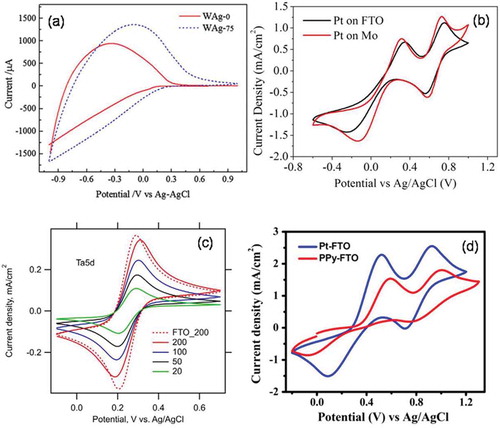
Cyclic voltammetry (C-V) technique has played an enormous role in the fabrication of different optoelectronic devices. It is used to determine the oxidation and reduction potentials of the different substrates and materials used in device fabrications. Common devices such as solar cells, transistors and especially batteries, capacitors and super capacitors have used C-V analyses to investigate the charge-discharge rates of the devices. Prior studies by (Hoseinzadeh et al., Citation2018; Jha et al., Citation2017; Sim et al., Citation2013) on the application of C-V measurements on substrates for electrochromic devices, photocatalysis, counter electrodes, etc. are available in literature. Hoseinzadeh showed the electrochromic properties of WO3 and WO3–Ag thin films using C-V tests. The transmittance was reported to increase in the WO3-Ag due to the Ag nanoparticles. The WO3 exhibited oxidation and reductions peaks at ~ −0.3 V compared to the WO3-Ag at ~-0.15 V. This led to an increase in current and improvement in the electrochromic properties of WO3-Ag films. Krysova et al., 2017 used C-V test to investigate the optical transmittance of Ta-doped TiO2 (anatase) thin films are grown on ordinary soda-lime glass substrate for photocatalytic applications. Similar technique by Sim et al, 2017 to measure the photocurrent conversion and performance of dye sensitize solar cells (DSSC) using molybdenum (Mo) and fluorine-doped-tinoxide (FTO) substrates. Very recently, flexible substrates from stainless steel coated with platinum (Pt) have also been used in other studies I addition to Polypyrrole (PPy) FTO‐coated glass substrate. These are used as the photoanodes in DSSCs. However, PPy-FTO substrates recorded lower performance compared to the Pt-FTO at the oxidation potentials of 0.32 and 0.28 V, respectively
This paper therefore reviews the effects of substrates on devices fabricated for optoelectronic applications. It includes the types and characteristics of substrates, synthesis and fabrication of substrates, and the influence of substrates on the optical properties, surface morphology and current-voltage behaviour of optoelectronic devices. Suggestions on new technologies and their future implications for the optoelectronic industries are presented.
2. Substrates and performance of optoelectronic devices
Recent studies have shown that the different techniques incorporated in the production of photovoltaic cells affect the device performance like the application of pressure during Organic photovoltaic (OPV) fabrication. In this example, device performance is improved when the surface contact between layers is enhanced due to the application of pressure (Agyei-Tuffour et al., Citation2016). Nevertheless, increasing pressure can also cause excessive sink in of particles trapped between the layers and further lead to a disruption in the performance of the devices just as low adhesion between layers can lead to interfacial failure (Oyewole et al., Citation2015). Despite degradation factors (Giannouli et al., Citation2015) and more, between 2009 and 2020, PV efficiencies have shown a rapid increase, especially in low-cost perovskite materials (See Figure ). However, the efficiency of perovskite cells drops at larger scales contrary to laboratory records set on small samples (Extance, Citation2019). Other substrates produced using the electrochemical depostion methods have been adopted in inverted optoelectronic devices such as OPV and OLEDs. Silver thin film on glass, ZnO-Al-ZnO, Pt/FTO, WO3-Ag films, etc. have been produced and their electrochromic properties investigated. Some of the common cyclic voltammograms are presented in Figure to the show the oxidation and reduction potentials of the electrode.
Figure 1. Cell efficiencies compilation. Adapted from Ref. (Bisquert Citation2017; Giannouli et al., Citation2015; CitationNational Renewable Energy Laboratory (NREL), 2020)
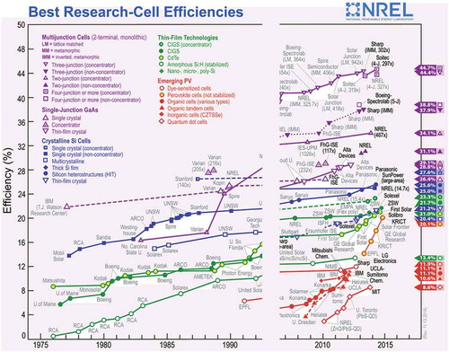
Figure 2. Cyclic voltammograms of: (a) WO3 and WO3–Ag thin films (b) Pt-coated FTO and Pt-coated Mo counter electrodes, (c) Ta5d sample (5%-Ta, 500 nm layer thickness) at scanrates 50, 100 and 200 mV/s. and (d) PPy‐FTO film and Pt‐FTO on glass (Hoseinzadeh et al., Citation2018; Jha et al., Citation2017; Krysova et al., Citation2017; Sim et al., Citation2013)
2.1. Characteristics of optoelectronic devices
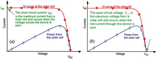
Important parameters utilized in the study of optoelectronic devices have been documented by Christiana Honsberg and Stuart Bowden in a survey to improve photovoltaic education include short-circuit current, open-circuit voltage, fill factor and cell efficiency. (Honsberg & Bowden, Citation2017)
The current that goes through the device when the voltage across it is zero is called the short-circuit current (ISC) (Figure ). The ISC equation is:
where Isc is the short circuit current over the area of the device,
q is the fundamental unit of charge,
Ln and Lp are the electron and hole diffusion lengths respectively, and
G is the generation rate.
Open-circuit voltage, VOC is the maximum voltage available from the device when there is no current (Figure ). The VOC equation is given as
where is the thermal voltage,
is the doping concentration,
is the excess carrier concentration, and
is the intrinsic carrier concentration.
Fill Factor (FF) is a conjugated parameter which determines the maximum power provided by a PV. FF relation is given as
where the VOC is normalized to
The cell efficiency is defined as the ratio of the energy output from the PV to the input energy from the sun. This parameter reflects the performance of the PV to the light spectrum, incident sunlight intensity and the PV temperature. The
relationship to the incident power
is given by the following equations:
where all terms have their usual meaning.
Figure 3. (a) and (b) represent the current-voltage (IV) characteristic graph of a PV indicating the ISC and VOC respectively. Adapted from Ref. (Honsberg & Bowden, Citation2017)
3. Substrate materials and optoelectronic devices fabrication methods
A substrate mostly refers to a slice of semiconducting material like silicon or metal oxide in computing and electronics. (Duan et al., Citation2003; Rogers et al., Citation2009) Substrates serve as the foundation for the fabrication of components such as integrated circuits and transistors. Materials used for substrates are cut to form thin discs, sometimes called wafers, on which other electronic components are constructed. (Isa et al., Citation2009) Vacuum vapor deposition methods used mostly for substrate fabrication and deposition makes them light, flexible and non-oxidizing in air. (Jean et al., Citation2016; Montanino et al., Citation2015) Depending on the industry involved, the substrate material could differ, so the various types of substrates used based on the device configuration or fabrication parameters could be rigid or flexible depending on the intended purpose. (Mortimer et al., Citation2006; Rogers et al., Citation2009; Zardetto et al., Citation2011)
3.1. Classification of substrates
3.1.1. Rigid substrates
Rigid substrates are stiff, hard and inflexible materials on which electronic devices are applied. Since these materials are unbending, they are used in applications where flexibility is not a requirement. The most common rigid substrates used in optoelectronic technology are silicon, glass and metal.
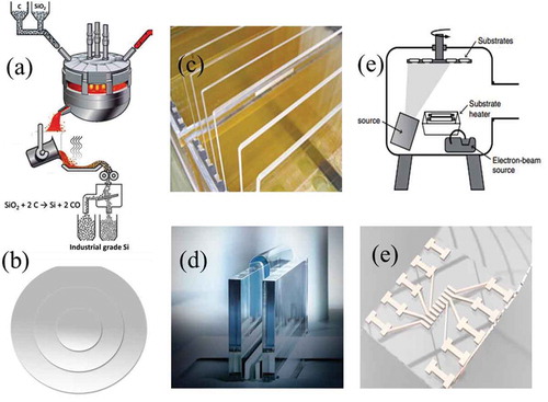
Silicon, unlike glass, is a semiconducting tetravalent metalloid with a blue-grey metallic outlook and the processing route into wafers and micro- and nanochips is shown in Figure . Though classified as hard, it is a brittle crystalline solid. In the universe, Silicon is the eighth most common element by mass. It is usually found in dust particles and grains of sand as silicon dioxide (quartz) or on planets and planetoids as silicate making it the most abundant element after oxygen. The reflective nature of Silicon and the ability to control its charge carriers to obtain desired electrical properties are desirable properties in the optoelectronics industry (Asim et al., Citation2012; Iwata et al., Citation2001). The glass, on the other hand, is a thermally stable amorphous solid that has application in tableware optoelectronics and many others. Properties of glass include reflection, refraction, and transmission. Glass cannot scatter light because it lacks grain boundaries. This makes it a desired material in the manufacture of devices such as lenses and windowpanes. The refractive index of simple glass is around 1.5 and can be altered by integrating with low or high-density materials such as boron, lead oxide, zirconium, titanium and barium. Inherent features of glass that limit its applications include rigidity, heaviness, and brittleness (N. Wang et al., Citation2012).
However, Flaherty et al, (Citation2017) developed a flexible glass substrate for organic printed electronics and solar cells. Again, most metal substrates are considered rigid and their smoothness can be enhanced by polishing or by applying other layers. The conductive nature of these metal substrates can be either advantageous or disadvantageous. When metal substrates are used for back contacts in thin-film electronics, their conductive properties are not utilized. Such substrates are mostly insulated from interacting with the device using a laminating or insulating layer. For instance, due to stainless steel’s inability to undergo oxidation, it can be used as a dimensionally stable substrate in OPV devices to prevent degradation. In this case, also, foils made of stainless steel have been used as flexible substrates. (Flint et al., Citation2000; Galagan et al., Citation2012; Yu et al., Citation2003; Miettunen et al., Citation2008)
Figure 4. (a) Silicon production (Kero et al., Citation2017) (b) Silicon films/wafers (Choung et al., Citation2016; LABTECH, Citation2020; Taguchi et al., Citation2014) (c) ultrathin glass substrate (Flaherty, Citation2017) (d) Sketch of a vacuum deposition process (Angus Macleod, Citation2013) (e) electronic devices integrated unto a glass film/substrate (Novacentrix, Citation2020)
3.1.2. Flexible substrates
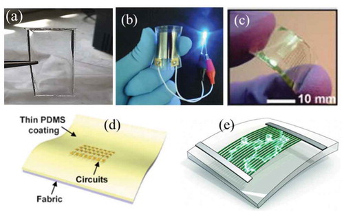
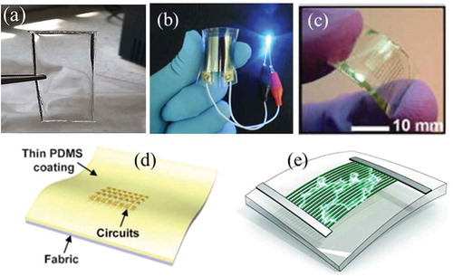
Flexible materials or substrates that could replace rigid substrates for applications in electronics would include polymer substrates, plastic substrates and/or elastic substrates. (Duan et al., Citation2003; Rogers et al., Citation2009). Flexural properties of such materials make them a preferred choice over transparent rigid substrates owing to their lightweight, bending ability (V. Kumar & Wang, Citation2013) and their compatibility with the large-scale roll-to-roll production process. (Asare et al., Citation2015, Citation2017; Dupont et al., Citation2012; Jouane et al., Citation2013; Kayser & Lipomi, Citation2019; Popoola et al., Citation2017; Van de Wiel et al., Citation2013; Weber et al., Citation2018). For transparent flexible substrates used in OPVs, inertness to organic solvents, excellent optical performances, low coefficient of thermal expansion (CTE) and thermal durability are definite requirements. Such transparent bendable or stretchable polymer substrates include polydimethylsiloxane (PDMS), polyethylene terephthalate (PET), polyimide (PI) Foil, polycarbonate (PC), polyethylene 2,6-naphthalate (PEN), polyethersulfone (PES), nanocellulose and metallic foils. (Agyei-Tuffour et al., Citation2016; Kaltenbrunner et al., Citation2012; Razzell-Hollis et al., Citation2013)
In terms of application, polydimethylsiloxane (PDMS) is the most utilized organic polymer substrate in the organic electronics industry. It is known for its extraordinary flow properties, non-flammability, high optical transmittance, inertness, and non-toxic nature. (Wypych, Citation2016) This viscoelastic silicon-based polymer is applied in various capacities from contact lenses and medical devices to elastomers; it is also present in shampoos, food, caulk, lubricants and heat-resistant tiles. (Barth-Wehrenalp & Block, Citation1963; Duffy et al., Citation1998; McDonald & Whitesides, Citation2002).Polyethylene-terephthalate (PET) is another generally useful flexible substrate applied in devices that require chemical and thermal resistant features as well as transparency (Hwang et al., Citation2009). PET stands out as the most familiar thermoplastic polymer resin of the polyester family and is often used in fibers for clothing, solid and liquid food containers, thermoforming for manufacturing, and composites with glass fiber for engineering resins. Most PET production is directed towards artificial/synthetic fibres with bottle production accounting for about 30% of the demand. It is also applied in textiles and packaging materials. (Aleksandrova et al., Citation2015; Cho et al., Citation2008; Hwang et al., Citation2009; Kuwabara et al., Citation2012; Li et al., Citation2017; Li et al., Citation2005; Moro et al., Citation2012; Part et al., Citation2014; Sun et al., Citation2010; Yu et al., Citation2016).Polyimide is a polymer of imide monomers. Registering high heat-resistances, polyimides afford diverse applications in parts that require unrefined organic materials such as high-temperature fuel cells, displays, and many military roles. (Ding et al., Citation2011; Li et al., Citation2017)
A group of thermoplastic polymers called Polycarbonate (PC) is a tough material with some grades being optically transparent. PCs are widely applied in flexible electronics since they can be easily molded and thermoformed. (Ahmad et al., Citation2013; Ho et al., Citation2014, Citation2012; Chen et al., Citation2007).Polyethersulfone (PES) forms part of the three Polysulfones used industrially for electrical equipment and medical technology (Kayser & Lipomi, Citation2019). Polysulfones, with a glass transition temperature of 185°C, is composed of para-linked aromatics, sulfonyl groups and ether groups and partly also alkyl groups. Their raw material and processing cost is high and is mostly used in specialty applications. Substrates made of PES are expected to have outstanding resistance to heat and oxidation. PES is resistant to hydrolysis in aqueous and alkaline media. These properties along with their good electrical properties make them a good source of substrate material in optoelectronic device fabrication. (Ashraf, Citation2015; Fink, Citation2008)
Paper’s multifarious applications and low cost make it an attractive material for substrate development. Paper is an ecofriendly and cheap material for many electronic applications such as the fabrication of substrate for integrated waveguides and electronic circuit ink-jet printing. (Kumar et al., Citation2016; Moro et al., Citation2012). However, it poses serious challenges in electronics due to its high optical haze and low transmittance property. In optoelectronic devices, the major concern is to increase the efficiency of light coupled into and out of the paper substrate. The combination of paper and plastic materials to form plastic-paper substrate (See Figure ) has solved this problem by increasing the optical and haze transmittances to >85% and >90% respectively in a broadband wavelength (Yao et al., Citation2016). Aside from the mechanical flexibility, this new substrate is also ultra-flat and very compatible with optoelectronic device fabrication processes. (Park et al., Citation2016; Yao et al., Citation2016) Nanocellulose and 3 M™ tape materials are also used to replace conventional conducting substrates in fabricating highly efficient stretchable organic PV devices. These materials shown in Figures and , pave ways for fully deformable PVs in wearable electronics (Chen et al., Citation2017; Costa et al., Citation2016). Finally, Metal foil substrates are predominantly used for flexible organic electronic devices. These substrates are particularly attractive in organic electronics because they provide excellent barriers to water and oxygen leading to an increase in the life span of the device. (Galagan et al., Citation2012) Stainless steel foil is mostly used in manufacturing OPVs because of its superior chemical resistance to other chemicals used in the fabrication process. (Galagan et al., Citation2012)
Figure 5. (a) paper (b) a schematic showing Yao et al’s potential roll-to-roll fabrication of transparent plastic-paper substrates. Reprinted from ref. (Yao et al., Citation2016) (c) & (d) are the optimized combination of high transmittance (similar to plastic) and high transmission haze of plastic-paper substrates. Reprinted from ref. (Yao et al., Citation2016)
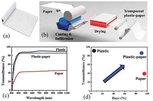
Figure 6. (a) ITO on PET thin film substrate (b) A film bulk acoustic resonator with Au electrodes on a PET substrate. Reprinted from ref. (Yu et al., Citation2016) (c) Polyimide film (DuPont, Citation2017) (d) Polycarbonate film (Pc-film, Citation2020) (e) Nanocellulose film (Smy.fi, Citation2016) (f) M tape (AlCO, Citation2020)
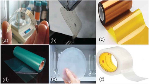
Figure 7. (a) Polydimethylsiloxane (PDMS) film and (b)-(e) are some flexible and stretchable electronic devices integrated unto a PDMS film. Reprinted from ref. (Kim et al., Citation2009; Lin et al., Citation2014; Menard et al., Citation2005; Qi et al., Citation2010; Yoon et al., Citation2008; Zhou et al., Citation2019)
3.2. Substrate effect on perovskite solar cells performance
The performance of perovskite-based solar cells fabricated on different substrates has seen a steady rise over the years (Fan et al., Citation2017; Green et al., Citation2014; Qiu et al., Citation2018; Szuromi & Grocholski, Citation2017). Lal et al., (Citation2017) reported on the development of perovskite tandem cells on rigid substrates (FTO coated glass), major motivations and challenges. Recently, perovskite solar cells have also been deposited on a flexible substrate (PET/ITO) with ~19.11% efficiency (Suk Jung et al., Citation2019). The influence of the flexible substrates opens a myriad of mechanical effects on the device performance such as folding, bending and stretching.
The impacts and challenges associated with these multiple mechanical effects on flexible optoelectronics have been addressed by Sukjung et al.,2019 in a similar review article. The combined efforts to increase efficiency and achieve appreciable stability of the device has led to tandem cells produced to utilize the energy of short-wave photons in the light spectrum (Lal et al., Citation2017). The tandem cells were possible following the previous report by N.G. Park (Citation2015) on the optoelectronic properties of perovskite materials and progress made in achieving commercial-scale perovskite solar cells. Initially, an ~10% efficient perovskite solar cells were re-developed, and the solid hole conductor was substituted with a liquid electrolyte leading to an ~18% efficiency in just two years. It was further suggested that future technologies should employ encapsulation to achieve environmental and photo-stability (Park, Citation2015). The encapsulation could be done with PDMS or other suitable materials reviewed in this paper.
Recently, Zhao and Chen et al reported a bulk passivation strategy by incorporating 2.5% chlorine which increased crystallinity leading to larger grains and reduced electronic disorder in mixed tin-lead low-bandgap (~1.25 eV) perovskite layers leading to increased carrier mobility. This allowed low band-gap perovskites with power conversion efficiencies of 21% and steady-state efficiencies (20.7%) to be fabricated. The efficiencies, in this case, was retained to 85% after 80 hours of operation (Lin et al., Citation2018; Zhao et al., Citation2018). Wali and Elumalai et al also reviewed the progress made on tandem solar cells and comparisons were made between multiple and single junction tandem cells. The advantages, breakthroughs, limitations, current developments and future potential for practical applications of the perovskite solar cells were also presented (Wali et al., Citation2018). Anaya et al., 2017 again investigated the use of metal halide (ABX3) as an active layer for tandem solar cells. ABX3 perovskite was found to be easily fabricated, less expensive and exhibiting outstanding optical and electronic properties. Therefore, ABX3 perovskites were found to be good candidates for large scale green energy production.
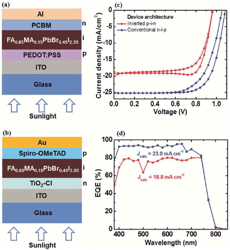
Metal halide tandem cells studies by Shen et al, 2018 and Doung et al., have reported efficiencies of ~ 26.4 % for a four-terminal cell configuration. The new prospects of tandem structures were studied and key aspects and challenges such as device toxicity and stability were addressed in the study. The stability issues in perovskites have been tackled by investigating and optimizing the individual layers in the perovskite solar cell including their reaction with water. Device encapsulation using water-resistant materials to protect the devices from degradation have been reported by (Kim et al., Citation2010; Wang et al., Citation2016). When Planar and or textured substrates are used, the current-voltage characteristics of fabricated perovskite solar cell can be very significant. Reports by Biao Shi et al. (Citation2017) in Figure , Suk Jung et al. (Citation2019) in Figure , Adjokatse et al. (Citation2019) in Figure showed that the textured fluorine-doped tin oxide (FTO) produced highly efficient devices of ~ 20 mA/cm2 compared to ~17.5 mA/cm2 in the smooth FTO substrate device. Device architecture and substrates have also been discovered to influence performance. As shown in Figure , the conventional architecture using indium tin oxide (ITO) coated glass substrate was higher compared to the inverted architecture.
Figure 8. Smooth and textured FTO substrates and the current-voltage behaviour in perovskite solar cells. (Adapted from (Shi et al., Citation2017))
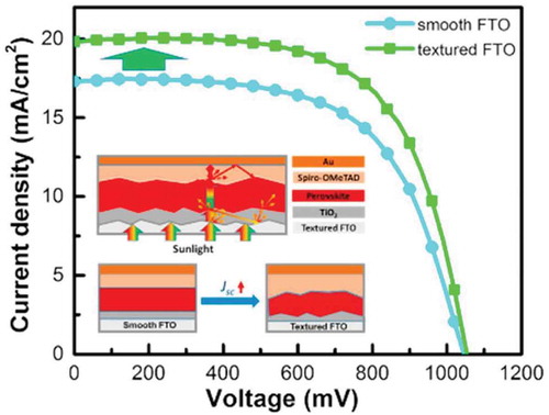
Figure 9. Perovskite film produced using additives (a) Schematic illustration of the different morphology development for CH3NH3PbI3_xClx films with and without H2O additive. (b) Illustration of the F-PSC structure and J–V curves of F-PSCs under both reverse and forward scan directions using MAPbI3–DS (dimethyl sulfide) as the absorber layer. (c) Cross-sectional SEM image and J-V curves of an F-PSC with the Rb1K4CsFAMA absorber. (Suk Jung et al., Citation2019)
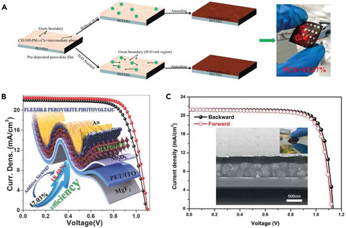
Figure 10. Different substrate architecture and their effect on FAI-based perovskite solar cell performance; (a) PEDOT.PSS based hole transport layer based substrate architecture, (b) TiO2-Cl hole transport layer based substrate architecture. (c) and (b) are the performance measurements (Adjokatse et al., Citation2019)
3.3. Influence of substrate on morphological properties of optoelectronic device layers
The substrate used in the fabrication of optoelectronic devices may have significant impacts on the nano- and micro-morphological properties and the performance of devices. The relationship between solar cell performances and surface morphology of substrates are shown in Figure (Chen et al., Citation2019; Li et al., Citation2019, Yang et al., Citation2019; Gusain et al., Citation2019; Nasuno et al., Citation2001). Chen et al reported on using air-stable vacuum-assisted and high relative humidity to control the morphology on the glass substrate. Li et al showed the challenges and strategies on the perovskite’s morphology and their performance whereas Yang et al studied perovskites with planar morphologies with complex tin (IV) oxides. Figures show the interfacial processes and morphologies that influence solar cell performance. In organic solar cells, using a textured-ZnO substrate and µc-Si: H fabricated through the wet etching process to get the optimum morphology of the substrate would give high efficiency according to Nasuno et al. An average slope, tan θ, of substrate surface textures, was achieved by atomic force microscopy (AFM) images and solar cell performance was matched with tan θ. The balance between the optical confinement and the grain boundary formation generated a conversion efficiency as a maximum at a tan θ of 0.08 which was 3 times less as compared to that of a α-Si: H substrate. When the optimized morphology was used, an efficiency of 9.4% was obtained at a deposition temperature of 140°C (Nasuno et al., Citation2001). Also, organic vapor phase deposition was used to grow polycrystalline pentacene channel thin-film transistors and X-ray diffraction showed that octadecyl trichlorosilane (OTS) treatment of the substrate before the deposition of pentacene decreased the order of the molecular stacking or increased the density of flat-lying molecules because of the improved hole mobility at the pentacene/OTS interface (Knipp et al., Citation2003; Shtein et al., Citation2002). Furthermore, graphene monolayers deposited on oxide substrates have been seen to have superior charge mobility and thermal transport due to the effects of substrate surface corrugation on the equilibrium mean thickness of the supported graphene and the interfacial adhesion energy. By considering both the substrate surface corrugation and the mismatch strain, it is found that a tensile mismatch strain reduces the corrugation amplitude of graphene whilst a corrugated substrate surface promotes strain-induced instability under a compressive strain.
Therefore, the morphology of supported graphene monolayers can be monitored or controlled (Aitken & Huang, Citation2010). Research work by Stakheev et al on metal–substrate interaction found that there were some substrate-induced effects in the form of electronic modifications of the supported clusters and morphological transformations (Stakheev & Kustov, Citation1999). Last but not least, the interface composition was found to be linked to the surface energy of the substrate upon which the polymer-fullerene blends are cast according to work done by Germack et al and Agyei-Tuffour et al (Agyei-Tuffour et al., Citation2017, Citation2016; Germack et al., Citation2009).
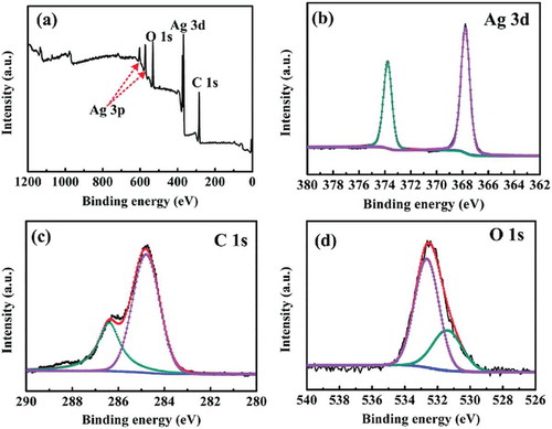
X-ray photoelectron spectroscopy (XPS) is a very important surface characterization technique to investigate the surface and elemental composition of thin films used in the optoelectronic device fabrications. Figure ) shows the XPS results of indium tin oxide (ITO) substrate treated with plasma oxidation, Zhang et al. (Citation2014). The binding energy peak showed at 529.7 eV is due to the oxygen in oxide lattice of the ITO. Similar XPS analyses of Silver substrates have also been studied by Mou et al. (Citation2018) in Figure ) and peaks with varying intensities against the binding energy for the common elements such as Ag3d3/2, Ag3d5/2 were recorded at 367.8 eV and 373.8 eV respectively. These correspond to the pure Ag element without the formation of an oxide on the surface. The O1s peaks at 531.4 eV and 532.6 eV refer to the adsorbed oxygen from the environment.
Figure 11. (a) A 3D schematic view of a perovskite based Photovoltaic cell, (b) cross-sectional SEM view of perovskite based Photovoltaic on an FTO coated glass, (c) morphology of perovskite on a glass slide under stable air deposition method and (d) morphological view of the perovskite layer on glass under vacuum flash assisted method of deposition. (Chen et al., Citation2019)
Figure 12. Surface morphology challenges of high performing inorganic perovskite solar fabrication; (a) pre-annealing technique, (b) spin-coating and (c) vacuum chamber deposition (Li et al., Citation2019)
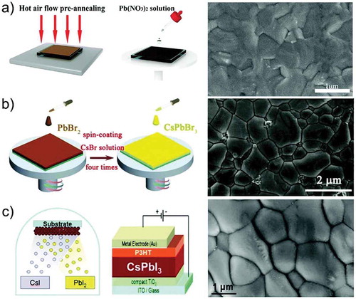
Figure 13. Planar structured solar cells with complex SnO2 and their performances; (a) and (b) are XRD images indicating peaks of SnO2 composites, (c) AFM images of three SnO2 based substrates, (d) band diagram of multilayers, (e) transmittance measurements for different substrate compositions (f) and electrical performances of different substrate configurations (Yang et al., Citation2018)
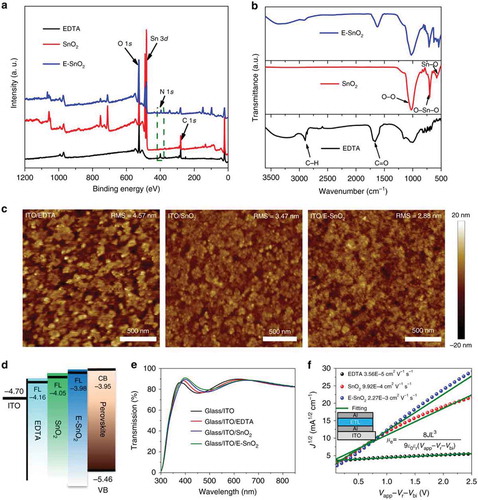
Figure 14. (a), (b), (c) and (d) show interfacial processes and performance challenges in polymer solar cells; (Agyei-Tuffour et al., Citation2017; Gusain et al., Citation2019)
Figure 15. O1s XPS analysis of (a) pristine ITO; (b) plasma-treated ITO. (Zhang et al., Citation2014)
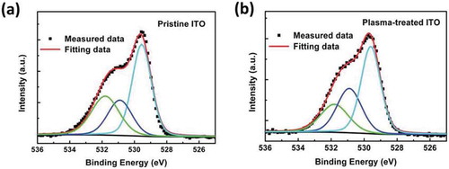
Figure 16. XPS spectra of silver film on glass substrate sintered at 110 °C for 2 h: (a) survey spectrum, (b) Ag3d spectrum, (c) C1s spectrum, and (d) O1s spectrum. (CitationMou et al., 2018)
4. Conclusions and recommendations
This review article presented the effects of substrates on the morphology and performance of optoelectronic devices. The study showed that there are two major types of substrates used in the optoelectronic industry. They are planar and textured substrates. These can also be classified as rigid or flexible depending on the Youngs moduli and flexural properties of the substrate. Planar and rigid substrates such as glass and metals are used where stretching and or bending are not required. Textured and flexible substrates are used where deformation in bending, stretching and in some cases, torsion is required. Planar substrates usually result in low light harvesting, reduced optical absorption and hence low device efficiencies compared with textured substrates. This is largely due to the fact that, there are enhanced reflections of the incident radiations on planar substrates. Textured substrates allow for multiple internal reflections and therefore increase the residence time of the incident radiation. The study again showed that planar substrates usually induce smooth surface morphologies at the intra- and interfacial surface contacts between the layered structures whereas textured substrates leads to corrugated or relatively rough morphologies. These rough morphologies are responsible for multiple light scatterings in optoelectronic devices hence lead to improved performances. They also lead to molecular re-configuration in both edge-on and face-on stacking. For example, poly-3-hexylthiophene molecules will assume edge-on configuration on planar glass substrates and both edge-on and face-on configuration on textured substrates.
It is recommended that textured substrates with high mechanical flexibility can be adopted in large-area optoelectronic device frabrications due to their versatility in applications including wearable electronics, ultra-thin devices, corrugated optoelectronic roofing structures and many more. These also clearly points to the challenges and opportunities for further research in the field of optoelectronic device materials and fabrication techniques.
Cover Image
Source: Author.
Acknowledgements
The preparation of this article was supported by the University of Ghana Building a New Generation of Academics in Africa (BANGA-Africa) Project with funding from the Carnegie Corporation of New York. The statement made and views expressed are solely the responsibility of the authors.
Additional information
Funding
Notes on contributors
Joseph Asare
Joseph Asare researches into device physics, organic and perovskite photovoltaic cells using computational and experimental techniques with the Department of Physics, University of Ghana.
Benjamin Agyei-Tuffour
Benjamin Agyei-Tuffour, Emmanuel Nyankson and Bismark Mensah are Researchers in the Department of Materials Science and Engineering.
Dr. Agyei-Tuffour is also a Carnegie and BANGA-Africa Fellow. The research interests are in Silicon Solar Cells, Organic and Perovskite Solar Cells, Composite Materials for Energy Generation and Storage, Oil and Gas, Sensors, Advanced Polymers, Water Purification, Environment and Construction.
Evangeline A. Amonoo
Evangeline Abena Amonoo is a PhD student at the Arizona State University. She obtained her undergraduate degree from the Department of Materials Science and Engineering, University of Ghana.
David Dodoo-Arhin
David Dodoo-Arhin, Abu Yaya and Boateng Onwona-Agyeman are Associate Professors in Materials Science and Engineering and research into conducting polymers, sensors, device fabrication, energy generation and storage.
Emmanuel Nyankson
Benjamin Agyei-Tuffour, Emmanuel Nyankson and Bismark Mensah are Researchers in the Department of Materials Science and Engineering.
Bismark Mensah
Benjamin Agyei-Tuffour, Emmanuel Nyankson and Bismark Mensah are Researchers in the Department of Materials Science and Engineering.
Oluwaseun O. Oyewole
Oluwaseun Oyewole researches into Organic and Perovskite Optoelectronic Devices as an Assistant Research Professor.
Abu Yaya
David Dodoo-Arhin, Abu Yaya and Boateng Onwona-Agyeman are Associate Professors in Materials Science and Engineering and research into conducting polymers, sensors, device fabrication, energy generation and storage.
Boateng Onwona-Agyeman
David Dodoo-Arhin, Abu Yaya and Boateng Onwona-Agyeman are Associate Professors in Materials Science and Engineering and research into conducting polymers, sensors, device fabrication, energy generation and storage.
References
- Adjokatse, S., Kardula, J., Fang, H. H., Shao, S., Ten Brink, G. H., & Loi, M. A. (2019). Effect of the device architecture on the performance of FA 0.85 MA 0.15 PbBr 0.45 I 2.55 planar perovskite solar cells. Advanced Materials Interfaces, 6(6). https://doi.org/10.1002/admi.201801667
- Agyei-Tuffour, B., Doumon, N. Y., Rwenyagila, E. R., Asare, J., Oyewole, O. K., Shen, Z., Petoukhoff, C. E., Zebaze Kana, M. G., O’Carroll, D. M., & Soboyejo, W. O. (2017). Pressure effects on interfacial surface contacts and performance of organic solar cells. Journal of Applied Physics, 122(20), 205501. https://doi.org/10.1063/1.5001765
- Agyei-Tuffour, B., Rwenyagila, E. R., Asare, J., Kana, M. G. Z., & Soboyejo, W. O. (2016). Effects of pressure on nano- and micro-scale morphological changes in conjugated polymer photovoltaic cells. Journal of Materials Research, 31(20), 3187–22. https://doi.org/10.1557/jmr.2016.344
- Ahmad, J., Bazaka, K., Anderson, L. J., White, R. D., & Jacob, M. V. (2013). Materials and methods for encapsulation of OPV: A review. Renewable and Sustainable Energy Reviews, 6(27), 104–117. https://doi.org/10.1016/j.rser.2013.06.027
- Aitken, Z. H., & Huang, R. (2010). Effects of mismatch strain and substrate surface corrugation on morphology of supported monolayer graphene. Journal of Applied Physics, 107(12), 123531. https://doi.org/10.1063/1.3437642
- AlCO. (2020). 3MTM 4828 PE Tape transparent all weather 48 mm x 25 mm [www.shop.alco.ch]. shop.alco.ch. https://shop.alco.ch/en/adhesive-tapes/549-3m-4828-pe-tape-transparent-all-weather-48mmx25m-5005111198046.html?search_query=3M+tape&results=172
- Aleksandrova, M., Andreev, S., & Kolev, G. (2015). Spray deposition of organic electroluminescent coatings for application in flexible light emitting devices. Cogent Engineering, 2(1), 1–8. https://doi.org/10.1080/23311916.2015.1014248
- Anaya, M., Lozano, G., Calvo, M. E., & Míguez, H. (2017). ABX3 perovskites for tandem solar cells. Joule., 1(4), 769–793. https://doi.org/10.1016/j.joule.2017.09.017
- Angus Macleod, H. (2013). Recent developments in deposition techniques for optical thin films and coatings. In Optical thin films and coatings: From materials to applications (pp. 3–25). Woodhead Publishing Limited. https://doi.org/10.1533/9780857097316.1.3
- Arpin, K. A., Mihi, A., Johnson, H. T., Baca, J. A., Rogers, J. A., Lewis, J. A., & Brann, P. V. (2010). Multidimensional architectures for functional optical devices, Advanced Materials, 22(10), 1084–1101. https://doi.org/10.1002/adma.200904096.
- Asare, J., Agyei-Tuffour, B., Oyewole, O. K., Zebaze-Kana, G. M., & Soboyejo, W. O. (2015). Deformation and failure of bendable organic solar cells. Advanced Materials Research, 1132(1), 116–124. https://doi.org/10.4028/www.scientific.net/amr.1132.116
- Asare, J., Türköz, E., Agyei-Tuffour, B., Oyewole, O. K., Fashina, A. A., Du, J., Kana, M. G. Z., & Soboyejo, W. O. (2017). Effects of pre-buckling on the bending of organic electronic structures. AIP Advances, 7(4), 045204. https://doi.org/10.1063/1.4975396
- Ashraf, M. R. (2015). Commodity polymers, engineering polymers and speciality polymers. academia.edu.
- Asim, N., Sopian, K., Ahmadi, S., Saeedfar, K., Alghoul, M. A., Saadatian, O., & Zaidi, S. H. (2012). A review on the role of materials science in solar cells. In Renewable and Sustainable Energy Reviews (Vol. 16, Issue 8, pp. 5834–5847). Elsevier. https://doi.org/10.1016/j.
- Barth-Wehrenalp, G., & Block, B. P. (1963). Inorganic polymers. Science (80-.), 142(3593), 627–632. https://doi.org/10.1126/science.142.3593.627
- Battalia, C., Escarie, J., Soderstrom, K., Erni, L., Ding, L., Bugnon, G., Billet, A., Boccard, M., Barraud, L., De Wolf, S., Haug, F.-J., Despeisse, M., & Ballif, C. (2010). Nanoimprint Lithography for High-Efficiency Thin-Film Silicon Solar Cells. Nano Letters, 11(2), 661. https://doi.org/10.1021/nl1037787
- Bisquert, J., Qi, Y., Ma, T., & Yan, Y. (2017). Advances and obstacles on perovskite solar cell research from material properties to photovoltaic function. ACS Energy Letters, 2(2), 520–523. https://doi.org/10.1021/acsenergylett.7b00085
- Chen, C. P., Chiang, C. Y., Yu, Y. Y., Hsiao, Y. S., & Chen, W. C. (2017). High-performance, robust, stretchable organic photovoltaics using commercially available tape as a deformable substrate. Solar Energy Materials & Solar Cells, 165(35), 111–118. https://doi.org/10.1016/j.solmat.2017.02.035
- Chen, L., Cao, H., Wang, S., Luo, Y., Tao, T., Sun, J., & Zhang, M. (2019). Efficient air-stable perovskite solar cells with a (FAI)0.46(MAI)0.40(MABr)0.14(PbI2)0.86(PbBr2)0.14 active layer fabricated: Via a vacuum flash-assisted method under RH > 50%.. RSC Advances, 9(18), 10148–10154. https://doi.org/10.1039/c9ra01625b
- Chen, T. N., Wuu, D. S., Wu, C. C., Chiang, C. C., Chen, Y. P., & Horng, R. H. (2007). Improvements of permeation barrier coatings using encapsulated parylene interlayers for flexible electronic applications. Plasma Processes and Polymers, 4(2), 180–185. https://doi.org/10.1002/ppap.200600158
- Chiang, C.-J., Winscom, C., Bull, S., & Monkman, A. (2009). Mechanical modeling of flexible OLED devices. Organic Electronics, 10(7), 1268–1274. https://doi.org/10.1016/j.orgel.2009.07.003
- Cho, S. W., Jeong, J. A., Bae, J. H., Moon, J. M., Choi, K. H., Jeong, S. W., Park, N. J., Kim, J. J., Lee, S. H., Kang, J. W., Yi, M. S., & Kim, H. K. (2008). Highly flexible, transparent, and low resistance indium zinc oxide-Ag-indium zinc oxide multilayer anode on polyethylene terephthalate substrate for flexible organic light light-emitting diodes. Thin Solid Films, 516(21), 7881–7885. https://doi.org/10.1016/j.tsf.2008.06.025
- Choi, M.-C., Kim, Y., & Ha, C.-S. (2008). Polymers for flexible displays: From material selection to device applications. Progress in Polymer Science, 33(6), 581–630. https://doi.org/10.1016/j.progpolymsci.2007.11.004
- Choung, R. S., Marietta, E. V., Van Dyke, C. T., Brantner, T. L., Rajasekaran, J., Pasricha, P. J., Wang, T., Bei, K., Krishna, K., Krishnamurthy, H. K., Snyder, M. R., Jayaraman, V., & Murray, J. A. (2016). Determination of B-cell epitopes in patients with celiac disease: Peptide microarrays. PLoS One, 11(1), 1–16. https://doi.org/10.1371/journal.pone.0147777
- Costa, S. V., Pingel, P., Janietz, S., & Nogueira, A. F. (2016). Inverted organic solar cells using nanocellulose as substrate. Journal of Applied Polymer Science, 133(28), 1-6. https://doi.org/10.1002/app.43679
- de Leeuw, D. M., & Cantatore, E. (2008). Organic electronics: Materials, technology and circuit design developments enabling new applications. Materials Science in Semiconductor Processing, 11(5–6), 199–204. https://doi.org/10.1016/j.mssp.2008.10.001
- Ding, D., Johnson, S. R., Yu, S.-Q., Wu, S.-N., & Zhang, Y.-H. (2011). A semi-analytical model for semiconductor solar cells. Journal of Applied Physics, 110(12), 123104. https://doi.org/10.1063/1.3671061
- Duan, X., Niu, C., Sahi, V., Chen, J., Parce, J. W., Empedocles, S., & Goldman, J. L. (2003). High-performance thin-film transistors using semiconductor nanowires and nanoribbons. Nature, 425(6955), 274–278. https://doi.org/10.1038/nature01996
- Duffy, D. C., McDonald, J. C., Schueller, O. J. A., & Whitesides, G. M. (1998). Rapid prototyping of microfluidic systems in poly(dimethylsiloxane). Analytical Chemistry, 70(23), 4974–4984. https://doi.org/10.1021/ac980656z
- DuPont, 2017. Summary of Properties [WWW Document]. DuPont TM Kapt. ® Summ. Prop. http://www.dupont.com/content/dam/dupont/products-and-services/membranes-and-films/polyimde-films/documents/DEC-Kapton-summary-of-properties.pdf%0Ahttp://www.dupont.com/content/dam/dupont/products-and-services/membranes-and-films/polyimde-films/documents/
- Dupont, S. R., Oliver, M., Krebs, F. C., & Dauskardt, R. H. (2012). Solar energy materials & solar cells interlayer adhesion in roll-to-roll processed flexible inverted polymer solar cells. Solar Energy Materials and Solar Cells, 97(1), 171–175. https://doi.org/10.1016/j.solmat.2011.10.012
- Extance, A. (2019). The reality behind solar power’s next star material. Nature, 570(7762), 429–432. https://doi.org/10.1038/d41586-019-01985-y
- Fan, R., Zhou, N., Zhang, L., Yang, R., Meng, Y., Liwei, L., Guo, T., Chen, Y., Xu, Z., Zheng, G., Huang, Y., Liang, L., Qin, L., Qiu, X., Chen, Q., & Zhou, H. (2017). Toward full solution processed perovskite/Si monolithic tandem solar device with PCE exceeding 20%. Solar RRL, 1(11), 1700149. https://doi.org/10.1002/solr.201700149
- Fink, J. K. (2008). High performance polymers. William Andrew Inc.
- Flaherty, N. (2017). Project develops flexible glass substrate for printed organic electronics. Eenewseurope. https://www.eenewseurope.com/news/project-develops-flexible-glass-substrate-printed-organic-electronics
- Flaherty, N. (2017). Project develops flexible glass substrate for printed organic electronics [WWW Document]. eenewseurope. https://www.eenewseurope.com/news/project-develops-flexible-glass-substrate-printed-organic-electronics
- Flint, S. H., Brooks, J. D., & Bremer, P. J. (2000). Properties of the stainless steel substrate, influencing the adhesion of thermo-resistant streptococci. Journal of Food Engineering, 43(4), 235–242. https://doi.org/10.1016/S0260-8774(99)00157-0
- Galagan, Y., Moet, D. J. D., Hermes, D. C., Blom, P. W. M., & Andriessen, R. (2012). Large area ITO-free organic solar cells on steel substrate. Organic Electronics, 13(12), 3310–3314. https://doi.org/10.1016/j.orgel.2012.09.039
- Germack, D. S., Chan, C. K., Hamadani, B. H., Richter, L. J., Fischer, D. A., Gundlach, D. J., & Delongchamp, D. M. (2009). Substrate-dependent interface composition and charge transport in films for organic photovoltaics. Applied Physics Letters, 94(23), 233303. https://doi.org/10.1063/1.3149706
- Giannouli, M., Drakonakis, V. M., Savva, A., Eleftheriou, P., Florides, G., & Choulis, S. A. (2015). Methods for improving the lifetime performance of organic photovoltaics with low-costing encapsulation. Chem Phys Chem, 16(6), 1134–1154. https://doi.org/10.1002/cphc.201402749
- Green, M. A., Ho-Baillie, A., & Snaith, H. J. (2014). The emergence of perovskite solar cells. Nature Photonics, 8(7), 506–514. https://doi.org/10.1038/nphoton.2014.134
- Gusain, A., Faria, R. M., & Miranda, P. B. (2019). Polymer solar cells-interfacial processes related to performance issues. Frontiers in Chemistry, 7 (61), 1–25. https://doi.org/10.3389/fchem.2019.00061
- Ho, Y. H., Liang, H., Liu, S. W., Tian, W. C., Chen, F. C., & Wei, P. K. (2014). Efficiency improvement of organic bifunctional devices by applying omnidirectional antireflection nanopillars. RSC Advances, 4(19), 9588–9593. https://doi.org/10.1039/c3ra46936k
- Ho, Y. H., Liu, S. W., Liang, H., Chen, F. C., Tian, W. C., & Wei, P. K., (2012). Luminous and conversion efficiency improvement in oled/opv tandem device with omnidirectional antireflection nanopillars. In Digest of technical papers - SID international symposium (pp. 1516–1519). https://doi.org/10.1002/j.2168-0159.2012.tb06101.x
- Honsberg, C., & Bowden, S., 2017. A collection of resources for the photovoltaic educator [WWW Document]. Copyr. 2019 PVeducation. https://www.pveducation.org/
- Hoseinzadeh, S., Ghasemiasl, R., Bahari, A., & Ramezani, A. H. (2017). The injection of Ag nanoparticles on surface of WO3 thin film: Enhanced electrochromic coloration efficiency and switching response. Journal of Materials Science: Materials in Electronics, 47(7). https://doi.org/10.1007/s11664-018-6199-4
- Hoseinzadeh, S., Ghasemiasl, R., Bahari, A., & Ramezani, A. H. (2018). Effect of post-annealing on the electrochromic properties of layer-by-layer arrangement FTO-WO3-Ag-WO3, Ag. Journal of Electronic Materials, 47(7), 3552–3559. https://doi.org/10.1007/s11664-018-6199-4
- Hwang, S. Y., Jung, H. Y., Jeong, J. H., & Lee, H. (2009). Fabrication of nano-sized metal patterns on flexible polyethylene-terephthalate substrate using bi-layer nanoimprint lithography. Thin Solid Films, 517(14), 4104–4107. https://doi.org/10.1016/j.tsf.2009.01.164
- Isa, T., Fujii, G., Morisue, M., & Kawamata, I. (2009). Semiconductor device, electronic device, and method of manufacturing semiconductor device. US Pat., 7(635), 889 36, https://doi.org/10.1007/s11664-018-6199-4.
- Iwata, N., & Okamoto, K. (2001). Non-Reflection Optical Fiber Termination and Method of Manufacturing the Same (Patent Application Pub. No. US 2001/0017971 A1). Washington, DC.
- Jean, J., Wang, A., & Bulović, V. (2016). In situ vapor-deposited parylene substrates for ultra-thin, lightweight organic solar cells. Organic Electronics, 31(31), 120–126. https://doi.org/10.1016/j.orgel.2016.01.022
- Jha, P., Veerender, P., Koiry, S. P., Sridevi, C., Chauhan, A. K., Muthe, K. P., & Gadkari, S. C. (2017). Growth of aligned polypyrrole acicular nanorods and their application as Pt‐free semitransparent counter electrode in dye‐sensitized solar cell. Polymers for Advanced Technologies, 30(31), 1–6. https://doi.org/10.1002/pat.4128
- Jouane, Y., Colis, S., Schmerber, G., Dinia, A., Lévêque, P., Heiser, T., & Chapuis, Y. A. (2013). Influence of flexible substrates on inverted organic solar cells using sputtered ZnO as cathode interfacial layer. Organic Electronics, 14(7), 1861–1868. https://doi.org/10.1016/j.orgel.2013.04.024
- Kaltenbrunner, M., White, M. S., Głowacki, E. D., Sekitani, T., Someya, T., Sariciftci, N. S., & Bauer, S. (2012). Ultrathin and lightweight organic solar cells with high flexibility. Nature Communications, 3(1), 1–7. https://doi.org/10.1038/ncomms1772
- Kayser, L. V., & Lipomi, D. J. (2019). Stretchable Conductive Polymers and Composites Based on PEDOT and PEDOT:PSS. Advanced Materials, 31(10), 1806133. https://doi.org/10.1002/adma.201806133
- Kero, I., Grådahl, S., & Tranell, G. (2017). Airborne Emissions from Si/FeSi Production. JOM, 69(2), 365–380. https://doi.org/10.1007/s11837-016-2149-x
- Kim, B. D., Kim, Y., Wu, J., Liu, Z., Song, J., Kim, H., Huang, Y. Y., Hwang, K., & Rogers, J. A. (2009). Ultrathin silicon circuits with strain-isolation layers and mesh layouts for high-performance electronics on fabric, vinyl, leather, and paper. Advanced Materials, 21(36), 3703–3707. https://doi.org/10.1002/adma.200900405
- Kim, Y., Cook, S., Tuladhar, S. M., Choulis, S. A., Nelson, J., Durrant, J. R., Bradley, D. D. C., Giles, M., Mc Culloch, I., Ha, C. S., & Ree, M. (2010). A strong regioregularity effect in self-organizing conjugated polymer films and high-efficiency polythiophene: Fullerene solar cells. In V. Dusastre, (Ed.), Materials for sustainable energy (Vol. 5, pp. 63–69). Nature Publishing Group, UK & Co-Published with Macmillan Publishers Ltd, UK. https://doi.org/10.1142/9789814317665_0009
- Knipp, D., Street, R. A., & Völkel, A. R. (2003). Morphology and electronic transport of polycrystalline pentacene thin-film transistors. Applied Physics Letters, 82(22), 3907–3909. https://doi.org/10.1063/1.1578536
- Krysova, H., Mazzolini, P., Casari, C. S., Russo, V., Bassi, A. L., & Kavan, L. (2017). Electrochemical properties of transparent conducting films of tantalum-doped titanium dioxide. Electrochimica acta, 232(1), 44–53. https://doi.org/10.1016/j.electacta.2017.02.124
- Kumar, A., Saini, G., & Singh, S. (2016). A review on future planar transmission line. Cogent Engineering, 3(1), 1–12. https://doi.org/10.1080/23311916.2016.1138920
- Kumar, V., & Wang, H. (2013). Selection of metal substrates for completely solution-processed inverted organic photovoltaic devices. Solar Energy Materials and Solar Cells, 113(1), 179–185. https://doi.org/10.1016/j.solmat.2013.02.010
- Kuwabara, T., Nakashima, T., Yamaguchi, T., & Takahashi, K. (2012). Flexible inverted polymer solar cells on polyethylene terephthalate substrate containing zinc oxide electron-collection-layer prepared by novel sol-gel method and low-temperature treatments. Organic Electronics, 13(7), 1136–1140. https://doi.org/10.1016/j.orgel.2012.03.015
- LABTECH. (2020, January 30). Micro-Tec standard silicon wafers and silicon chips [WWW Document]. Labtech Serv. Sci. https://www.labtech-em.com/em/silicon-wafers-substrates-and-specimen-supports
- Laconte, J., Iker, F., Jorez, S., André, N., Proost, J., Pardoen, T., Flandre, D., & Raskin, J.-P. (2004). Thin films stress extraction using micromachined structures and wafer curvature measurements. Microelectronic Engineering, 76(1–4), 219–226. https://doi.org/10.1016/j.mee.2004.07.003
- Lal, N. N., Dkhissi, Y., Li, W., Hou, Q., Cheng, Y. B., & Bach, U. (2017). Perovskite tandem solar cells. Advanced Energy Materials, 7(18), 1602761. https://doi.org/10.1002/aenm.201602761
- Li, B., Fu, L., Li, S., Li, H., Pan, L., Wang, L., Chang, B., & Yin, L. (2019). Pathways toward high-performance inorganic perovskite solar cells: Challenges and strategies. Journal of Materials Chemistry A, 7(36), 20494–20518. https://doi.org/10.1039/C9TA04114A
- Li, F., Shen, J., Liu, X., Cao, Z., Cai, X., Li, J., Ding, K., Liu, J., & Tu, G. (2017). Flexible QLED and OPV based on transparent polyimide substrate with rigid alicyclic asymmetric isomer. Organic Electronics, 51(12), 54–61. https://doi.org/10.1016/j.orgel.2017.09.010
- Li, Y., Tan, L. W., Hao, X. T., Ong, K. S., Zhu, F., & Hung, L. S. (2005). Flexible top-emitting electroluminescent devices on polyethylene terephthalate substrates. Applied Physics Letters, 86(15), 1–3. https://doi.org/10.1063/1.1900940
- Lin, Q., Huang, H., Jing, Y., Fu, H., Chang, P., Li, D., Yao, Y., & Fan, Z. (2014). Flexible Photovoltaic Technologies Qingfeng. Journal of Materials Chemistry C, 2(7), 1–13. https://doi.org/10.1039/c3tc32197e
- Lin, Y., Bai, Y., Fang, Y., Chen, Z., Yang, S., Zheng, X., Tang, S., Liu, Y., Zhao, J., & Huang, J. (2018). Enhanced thermal stability in perovskite solar cells by assembling 2D/3D stacking structures. The Journal of Physical Chemistry Letters, 9(3), 654–658. https://doi.org/10.1021/acs.jpclett.7b02679
- McDonald, J. C., & Whitesides, G. M. (2002). Poly(dimethylsiloxane) as a material for fabricating microfluidic devices. Accounts of Chemical Research, 35(7), 491–499. https://doi.org/10.1021/ar010110q
- Menard, E., Nuzzo, R. G., & Rogers, J. A. (2005). Bendable single crystal silicon thin film transistors formed by printing on plastic substrates. Applied Physics Letters, 86(9), 1–3. https://doi.org/10.1063/1.1866637
- Miettunen, K., Halme, J., Toivola, M., & Lund, P. (2008). Initial performance of dye solar cells on stainless steel substrates. The Journal of Physical Chemistry C, 112(10), 4011–4017. https://doi.org/10.1021/jp7112957
- Montanino, M., De Girolamo Del Mauro, A., Tesoro, M., Ricciardi, R., Diana, R., Morvillo, P., Nobile, G., Imparato, A., Sico, G., & Minarini, C. (2015). Gravure-printed PEDOT:PSS on flexible PEN substrate as ITO-free anode for polymer solar cells. Polymer Composites, 36(6), pp. pp. 1104–1109. https://doi.org/10.1002/pc.23486
- Moro, R., Bozzi, M., Collado, A., Georgiadis, A., & Via, S. (2012). Plastic-based Substrate Integrated Waveguide (SIW) components and antennas. In 2012 7th European microwave integrated circuit conference, Amsterdam, Netherlands (pp. 627–630).
- Moro, R., Bozzi, M., Kim, S., & Tentzeris, M. (2012). Novel inkjet-printed substrate integrated waveguide (SIW) structures on low-cost materials for wearable applications. 2012 42nd European microwave conference (pp. 72–75). https://doi.org/10.23919/EuMC.2012.6459165
- Mortimer, R. J., Dyer, A. L., & Reynolds, J. R. (2006). Electrochromic organic and polymeric materials for display applications. Displays., 27(1), 2–18. https://doi.org/10.1016/j.displa.2005.03.003
- Mou, Y., Cheng, H., Wang, H., Sun, Q., Liu, J., Yang Penga, Y., & Chen, M. (2018). Facile preparation of stable reactive silver ink for highly conductive and flexible electrodes. Applied Surface Science, 475(1). https://doi.org/10.1016/j.apsusc.2018.12.261
- Nasuno, Y., Kondo, M., & Matsuda, A. (2001). Effects of substrate surface morphology on microcrystalline silicon solar cells. Japanese Journal of Applied Physics, 2(Lett), 40. https://doi.org/10.1143/jjap.40.l303
- National Renewable Energy Laboratory (NREL). (2020). Best research cell efficiencies, Office of Energy Efficiency and Renewable Energy. U.S. Department of Energy. http://www.nrel.gov/ncpv/
- Novacentrix. (2020, February 13). Novacentrix ,NCC Nano, LLC. https://www.novacentrix.com/sites/default/files/GlassSlide_3.jpg
- Oyewole, O. K., Oyewole, D. O., Asare, J., Agyei-Tuffour, B., Zebaze Kana, M. G., & Soboyejo, W. O. (2015). Failure mechanisms in layers relevant to stretchable organic solar cells. Advanced Materials Research,1132(1), 106–115. https://doi.org/10.4028/www.scientific.net/amr.1132.106
- Park, N. G. (2015). Perovskite solar cells: An emerging photovoltaic technology. Materials Today, 18(2), 65–72. https://doi.org/10.1016/j.mattod.2014.07.007
- Park, Y., Nehm, F., Müller-Meskamp, L., Vandewal, K., & Leo, K. (2016). Optical display film as flexible and light trapping substrate for organic photovoltaics. Optics Express, 24(10), A974. https://doi.org/10.1364/oe.24.00a974
- Part, H., Noh, S. H., Yun, J. J., & Han, T. H. (2014). Vertical arrays of photoluminescent Alq3 nanotubes on flexible substrates by vapor deposition. Molecular Crystals and Liquid Crystals, 602(1), 193–199. https://doi.org/10.1080/15421406.2014.944763
- Pc-film, 2020. OMAY SE11 flame-retardant film [WWW Document]. Pc-film.com. http://pc-film.com/flamexretardantxxfilmsxxfrpcxfrppxppx/41.html
- Popoola, I. K., Gondal, M. A., & Qahtan, T. F. (2017). Recent progress in flexible perovskite solar cells: Materials, mechanical tolerance and stability. Renewable and Sustainable Energy Reviews, 82(1), 3127–3151. https://doi.org/10.1016/j.rser.2017.10.028
- Qi, Y., Jafferis, N. T., Lyons, K., Lee, C. M., Ahmad, H., & Mcalpine, M. C. (2010). Piezoelectric ribbons printed onto rubber for flexible energy conversion. Nano Letters, 10(2), 524–528. https://doi.org/10.1021/nl903377u
- Qiu, Z., Xu, Z., Nengxu, L., Zhou, N., Chen, Y., Wan, X., Liu, J., Ning, L., Hao, X., Bi, P., Chen, Q., Cao, B., & Zhou, H. (2018). Monolithic perovskite/Si tandem solar cells exceeding 22% efficiency via optimizing top cell absorber. Nano Energy, 53(1), 798–807. https://doi.org/10.1016/j.nanoen.2018.09.052
- Razzell-Hollis, J., Tsoi, W. C., & Kim, J. S. (2013). Directly probing the molecular order of conjugated polymer in OPV blends induced by different film thicknesses, substrates and additives. Journal of Materials Chemistry C, 1(39), 6235–6243. https://doi.org/10.1039/c3tc31245c
- Rogers, J. A., Ferreira, P. M., & Saeidpourazar, R. (2017). Non-Contact Transfer Printing (Patent No. US 9,555,644 B2). Illinois, US.
- Rogers, J. A., Khang, D.-Y., & Sun, Y. (2009). Stretchable form of single crystal silicon for high performance electronics on rubber substrates. US 7,521,292 B2.
- Rwenyagila, E. R., Agyei-Tuffour, B., Onogu, K. O., Akin-Ojo, O., Zebaze Kana, M. G., Alford, T. L., & Soboyejo., W. O. (2015). Computational modeling of optical properties in aluminum nanolayers inserted in ZnO for solar cell electrodes. Optics Letters, 40(16), 3914. https://doi.org/10.1364/OL.40.003914
- Rwenyagila, E. R., Agyei-Tuffour, B., Zebaze Kana, M. G., Akin-Ojo, O., & Soboyejo., W. O. (2014). Optical properties of ZnO/Al/ZnO multilayer films for large area transparent electrodes. Journal of Materials Research, 29(24), 2912–2920. https://doi.org/10.1557/jmr.2014.298
- Shi, B., Liu, B., Luo, J., Li, Y., Zheng, C., Yao, X., Fan, L., Liang, J., Ding, Y., Wei, C., Zhang, D., Zhao, Y., & Zhang, X. (2017). Enhanced light absorption of thin perovskite solar cells using textured substrates. Solar Energy Materials and Solar Cells, 27(1), 214–220. https://doi.org/10.1016/j.rser.2013.06.027
- Shtein, M., Mapel, J., Benziger, J. B., & Forrest, S. R. (2002). Effects of film morphology and gate dielectric surface preparation on the electrical characteristics of organic-vapor-phase-deposited pentacene thin-film transistors. Applied Physics Letters, 107(2), 268–270. https://doi.org/10.1063/1.3437642
- Sim, K., Sung, S.-H., Jo, H. J., Jeon, D.-H., Kim, D.-H., & Kang, J.-K. (2013). Electrochemical investigation of high-performance dyesensitized solar cells based on molybdenum for preparation of counter electrode. International Journal of Electrochemical Science, 8(6), 8272–8281. https://www.researchgate.net/publication/271197914
- Smy.fi. (2016). Nanofibrillar cellulose film [WWW Document]. Aalto Univ. https//smy.fi/en/products-services/nanocellulose-film-to-ease-performing-medical-tests/
- Stakheev, A. Y., & Kustov, L. M. (1999). Effects of the support on the morphology and electronic properties of supported metal clusters: Modern concepts and progress in 1990s. Applied Catalysis A: General, 188(1–2), 3–35. https://doi.org/10.1016/j.joule.2017.09.017
- Suk Jung, H., Sang Han, G., Nam-GyuPark, & JaeKo, M. (2019). Flexible perovskite solar cells. Joule, 3(8), 1850–1880. https://doi.org/10.1016/j.joule.2019.07.023
- Sun, L., Qin, G., Huang, H., Zhou, H., Behdad, N., Zhou, W., & Ma, Z. (2010). Flexible high-frequency microwave inductors and capacitors integrated on a polyethylene terephthalate substrate. Applied Physics Letters, 96(1), 013509. https://doi.org/10.1063/1.3280040
- Szuromi, P., & Grocholski, B. (2017). Natural and engineered perovskites. Science (80-.), 358(6364), 732–733. https://doi.org/10.1126/science.358.6364.732
- Taguchi, M., Yano, A., Tohoda, S., Matsuyama, K., Nakamura, Y., Nishiwaki, T., Fujita, K., & Maruyama, E. (2014). 24.7% Record efficiency HIT solar cell on thin silicon wafer. IEEE Journal of Photovoltaics, 4(1), 96–99. https://doi.org/10.1109/JPHOTOV.2013.2282737
- Van De Wiel, H. J., Galagan, Y., Van Lammeren, T. J., De Riet, J. F. J., Gilot, J., Nagelkerke, M. G. M., Lelieveld, R. H. C. A. T., Shanmugam, S., Pagudala, A., Hui, D., & Groen, W. A. (2013). Roll-to-roll embedded conductive structures integrated into organic photovoltaic devices. Nanotechnology, 24(48), 484014. https://doi.org/10.1088/0957-4484/24/48/484014
- Wake, M. C., Patrick, C. W., & Mikos, A. G. (1994). Pore morphology effects on the fibrovascular tissue growth in porous polymer substrates. Cell, Transplantation 4(4), 339–343. https://doi.org/10.1002/ppap.200600158
- Wali, Q., Elumalai, N. K., Iqbal, Y., Uddin, A., & Jose, R. (2018). Tandem perovskite solar cells. Renewable and Sustainable Energy , 84(1), 89–110. https://doi.org/Reviews10.1016/j.orgel.2009.07.003
- Wang, D., Wright, M., Elumalai, N. K., & Uddin, A. (2016). Stability of perovskite solar cells. Solar Energy Materials and Solar Cells, 147(1), 255–275. https://doi.org/10.1016/j.solmat.2015.12.025
- Wang, N., Zimmerman, J. D., Tong, X., Xiao, X., Yu, J., & Forrest, S. R. (2012). Snow cleaning of substrates increases yield of large-area organic photovoltaics. Applied Physics Letters, 101(13), 133901–133904. https://doi.org/10.1063/1.4754690
- Weber, S., Rath, T., Mangalam, J., Kunert, B., Coclite, A. M., Bauch, M., Dimopoulos, T., & Trimmel, G. (2018). Investigation of NiOx-hole transport layers in triple cation perovskite solar cells. Journal of Materials Science: Materials in Electronics, 70(3), 1847–1855. https://doi.org/10.1021/ac980656z
- White, M. S., Kaltenbrunner, M., Głowacki, E. D., Gutnichenko, K., Kettlgruber, G., Graz, I., Aazou, S., Ulbricht, C., Egbe, D. A. M., Miron, M. C., Major, Z., Scharber, M. C., Sekitani, T., Someya, T., Bauer, S., & Sariciftci, N. S. (2013). Ultrathin, highly flexible and stretchable PLEDs. Nature Photonics, 43(10), 811–816. https://doi.org/10.1016/S0260-8774(99)00157-0
- Wikipedia, 2017, January 26. Substrate (electronics) [WWW Document]. Wikipedia, Free Encycl. https://en.wikipedia.org/w/index.php?title=Substrate_(electronics)&oldid=765886040
- Wypych, G. (2016). PDMS polydimethylsiloxane. In Handbook of polymers (2nd Edn, pp. 340–344). ChemTec Publishing. https://doi.org/10.1016/b978-1-895198-92-8.50106-3
- Yang, D., Yang, R., Wang, K., Wu, C., Zhu, X., Feng, J., Ren, X., Fang, G., Priya, S., & Liu, S. (2018). High efficiency planar-type perovskite solar cells with negligible hysteresis using EDTA-complexed SnO2. Nature Communications, 9(3239), 1–11. https://doi.org/10.1038/s41467-018-05760-x
- Yang, Z., Yu, Z., Wei, H., Xiao, X., Ni, Z., Chen, B., Deng, Y., .. ....Beard, M. C., & Huang, J. (2019). Enhancing electron diffusion length in narrow-bandgap perovskites for efficient monolithic perovskite tandem solar cells. Nature Communications, 10(1), 1–9. https://doi.org/10.1038/s41467-019-12513–x
- Yao, Y., Tao, J., Zou, J., Zhang, B., Li, T., Dai, J., Zhu, M., Wang, S., Fu, K. K., Henderson, D., Hitz, E., Peng, J., & Hu, L. (2016). Light management in plastic–paper hybrid substrate towards high-performance optoelectronics. Energy & Environmental Science, 9(7), 2278–2285. https://doi.org/10.1039/c6ee01011c
- Yeung, T., Georges, P. C., Flanagan, L. A., Marg, B., Ortiz, M., Funaki, M., Zahir, N., Ming, W., Weaver, V., & Janmey, P. A. (2005). Effects of substrate stiffness on cell morphology, cytoskeletal structure, and adhesion. Cell Motility and the Cytoskeleton, 60(1), 24–34. https://doi.org/10.1002/cm.20041
- Yoon, J., Baca, A. J., Park, S., Elvikis, P., Geddes, J. B., Li, L., Kim, R. H., Xiao, J., Wang, S., Kim, T.-H., Motala, M. J., Ahn, B. Y., Duoss, E. B., Lewis, J. A., Nuzzo, R. G., Ferreira, P. M., Huang, Y., Rockett, A., & Rogers, J. A. (2008). Ultrathin silicon solar microcells for semitransparent, mechanically flexible and microconcentrator module designs. . Nature Materials, 7(11), 907–915. https://doi.org/10.1038/nmat2287
- Yu, J. C., Ho, W., Lin, J., Yip, H., & Wong, P. K. (2003). Photocatalytic activity, antibacterial effect, and photoinduced hydrophilicity of TiO 2 films coated on a stainless steel substrate. . Environmental Science & Technology, 37(10), 2296–2301. https://doi.org/10.1021/es0259483
- Yu, L., Jin, H., Hu, N., Dong, S., & Luo, J. (2016). Flexible film bulk acoustic resonators and filter-like structure made directly on polymer substrates. Integrated Ferroelectrics, 168(1), 157–162. https://doi.org/10.1080/10584587.2016.1159538
- Zardetto, V., Brown, T. M., Reale, A., & Di Carlo, A. (2011). Substrates for flexible electronics: A practical investigation on the electrical, film flexibility, optical, temperature, and solvent resistance properties. Journal of Polymer Science Part B, : Polymer Physics 13(9), 638–648. https://doi.org/10.1016/j.orgel.2012.03.015
- Zhang, C., Qi, L., Chen, Q., Lv, L., Ning, Y., Hu, Y., & Teng, F. (2014). Plasma treatment of ITO cathode to fabricate free electron selective layer in inverted polymer. Journal of Materials Chemistry C, 2014(2), 8715. https://doi.org/10.1039/C4TC01777C
- Zhao, D., Chen, C., Wang, C., Junda, M. M., song, Z., Grice, C. R., Yu, Y., Li, C., Subedi, B., Podraza, N. J., Zhao, X., Fang, G., Xiong, R. G., Zhu, K., & Yan, Y. (2018). Efficient two-terminal all-perovskite tandem solar cells enabled by high-quality low-bandgap absorber layers. Nature Energy, 3(12), 1093–1100. https://doi.org/10.1038/s41560-018-0278-x
- Zhou, H., Qin, W., Yu, Q., Cheng, H., Yu, X., & Wu, H. (2019). Transfer printing and its applications in flexible electronic devices. Nanomaterials, 9(283), 1–28. https://doi.org/10.3390/nano9020283