
 ?Mathematical formulae have been encoded as MathML and are displayed in this HTML version using MathJax in order to improve their display. Uncheck the box to turn MathJax off. This feature requires Javascript. Click on a formula to zoom.
Abstract
This paper describes a cryptographic protection system hardware device designed to improve data encryption and decryption performance and preserve data integrity. The cryptosystem is implemented by hardware-software method, where the encryption and decryption of data are carried out in a stand-alone FPGA device based on non-positional polynomial number system (NPN). For data encryption the next block of text to be encrypted is divided into sub-blocks and represented as separate binary polynomials and binary polynomials-keys are assigned to them, as well as irreducible polynomials (modules). Then, split blocks are calculated in parallel and a ciphertext is formed. For this purpose, the special algorithm where calculation of NPN parameters and check on irreducibility of polynomials (modules) and the program of generation of direct and inverse keys are developed and application functional is developed that implements operations in the ring of polynomials with coefficients GF(2) using an object-oriented approach. We have developed polynomial multipliers modulo sequential and parallel action (matrix multiplier) on the basis of which data encryption and decryption are performed.
PUBLIC INTEREST STATEMENT
For special-purpose transceiver devices, an autonomous portable hardware and software solution for information protection is required. For this task, the work used high-speed programmable logic integrated circuits designed to calculate complex mathematical operations. The algorithm is based on a non-positional polynomial number system (NPN). The source text, divided into blocks using a random number generator, is calculated in parallel and a ciphertext is formed. For this, a special algorithm has been developed, where the NPN parameters are calculated and polynomials (modules) irreducible and a program for generating direct and inverse keys is performed. Hardware multipliers of polynomials modulo sequential, parallel action (matrix multiplier) have been developed on the basis of which encryption and decryption of data is carried out.
1. Introduction
As means, methods and forms of automation of processes of gathering, storage and processing of information develop and become more complicated, its vulnerability increases. Hardware implementation of cryptosystems allows to protect autonomous digital devices from unauthorized access to classified information from the outside (Shan`gin, Citation2007). Many methods have been developed to meet the ever-increasing demand for secure communications, data storage, data transmission, etc. (Saini et al., Citation2020). One of the most reliable ways to solve the problem of data security in computer systems and networks is considered to be cryptographic protection, which provides the transformation of plain text into cipher text using cryptographic algorithms (RyabkoB & Fionov, Citation2004; Shan`gin, Citation2007).
Various algorithms and methods of data encryption are known. The use of reliable and effective non-traditional cryptographic methods, algorithms and software for information protection, for example, non-positional polynomial numbering systems or polynomial numbering systems in residual classes can provide fast and more time-efficient encryption methods, and increase the crypto stability of encryption algorithms. Moreover, it is possible to combine software and hardware implementation of encryption functions (Barrera et al., Citation2020; Aitkhozhayeva & Tynymbayev, Citation2014).
One of the significant advantages of hardware encryption (compared to software encryption) in modern information and communication technologies is its high performance (Gnatyuk et al., Citation2016). Besides, hardware implementation of cryptoalgorithm ensures its integrity, and encryption and key formation is performed in encryptor board itself, not in a computer memory. A second important advantage is that the implementation of an algorithm itself is protected. These advantages of hardware encryption have led to interest in hardware implementation of cryptosystems (Gnatyuk et al., Citation2016; Nedjah & de Macedomourelle, Citation2006; Sadiq & Ahmed, Citation2006; Tenca & Tawalbeh, Citation2003).
As modern security protocols become increasingly algorithm-independent, a high degree of flexibility with respect to cryptographic algorithms is desirable. A promising solution that combines high flexibility with the speed and physical security of traditional hardware is the implementation of cryptographic algorithms on reconfigurable devices such as FPGAs (Krishna et al., Citation2017; Liu et al., Citation2019; Wollinger et al., Citation2004; Zambreno et al., Citation2006).
Increasing efficiency of the encryption device with FPGA-based NPN is achieved by increasing the performance of encryption and decryption algorithms.
2. Materials and methods
In this work, FPGA-based data encryption and decryption algorithm was implemented. The cryptosystem algorithm, based on the multiplier of irreducible polynomials modulo (Kalimoldayev, Tynymbayev, Gnatyuk, Ibraimov et al., Citation2020; Kalimoldayev, Tynymbayev, Gnatyuk, Magzom et al., Citation2020; Kalimoldayev, et al., Citation2019), was implemented on Nexys 4 DDR FPGA board with parallel data computation. Nexys 4 DDR board is a complete, ready-to-use digital circuit design platform based on the Artix-7 programmable gate array (FPGA) from Xilinx. With a large, high-performance FPGA (part number Xilinx XC7A100T-1CSG324C), extensive external memory and a suite of USB, Ethernet and other ports, the Nexys4 DDR can accommodate designs ranging from input combinational circuits to powerful embedded processors.
The data encryption and decryption algorithm was designed and tested in the Xilinx ISE Design Suite 14.4 computer-aided design (CAD) and the hardware description language (HDL) Verilog was used. Some blocks and subblocks were written in VHDL. The multiplication of polynomials modulo irreducible polynomials was applied in this work, where multiplication is done with the analysis of lowest bits of multiplier.
The encryption and decryption algorithm has been tested in the ISE simulator (ISim). ISim provides a full-featured HDL simulator integrated into the ISE. A general block diagram of the encryption device is shown in .
Figure 1. General block diagram of encryption device (a) Software-hardware section; (b) Hardware section
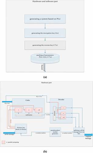
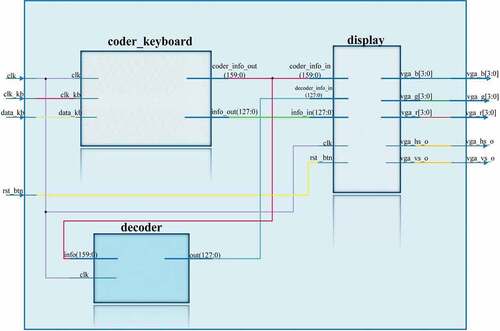
The RTL scheme of the main data encryption and decryption block is shown in . The main block consists of three main subblocks: coder_keyboard, decoder and display. The main coder_keyboardsubblock performs the function of forming the plaintext or source information and encrypting the generated data. The main decoder subblock is used to decrypt data. The main displaysubblock is used to visualize the encryption and decryption of the data. The main block has 4 inputs and 5 outputs. The first input of the main block clk is a 100 MHz clock signal. The inputs clk_kb and data_kbare used to read the scan code from the keypad. The input rst_btn resets the information in the monitor. The vga_b, vga_g, vga_r outputs are for shading the monitor. The horizontal and vertical sync signals vga_hs_o and vga_vs_oare used to send the hue of each pixel in the monitor.
Figure 2. RTL scheme of encryption and decryption implementation
shows the schematic of the main coder_keyboardsubblock for entering data into the buffer and encrypting data from the buffer.
Figure 3. RTL scheme of the main encryption subblock
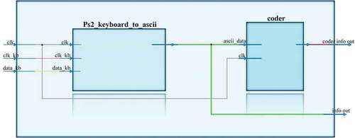
The main coder_keyboard subplot consists of several parts: coder, ps2_keyboard_to_ascii and buffered data generation. From the keyboard the data comes to ps2_keyboard_to_ascii, which converts the scan code to ascii code. Open text generation is done by scanning the data from the USB keyboard. The data is stored in a 128 bit or 16 byte buffer. If the buffer is not filled with keyboard data, it is filled with zeros. Each byte corresponds to each keyboard character, i.e. the maximum buffer size is 16 characters. It is possible to change the size of the initial information.
When a keyboard character is pressed, the output (ascii_new) of ps2_keyboard_to_ascii generates a press signal. When this signal is received the data buffer adds data from the ascii_data output. Pressing Enter sends information from the buffer to the coder block to encrypt the data. The BackSpace key removes data from the buffer character by character each time it is pressed.
A snippet of code written in Verilog to generate the raw data is given below:
always@ (negedgeascii_new)
begin
if(ascii_code = = 7*hOD)
info ≤ info_ram;
else if(ascii_code = = 7*h08)
info_ram≤ info_ram≫8;
else
info_ram≤ {info_ram,{1ʹb0, ascii_code}};
end
assign info_out = info_ram;
always @ (posedgeclk)
clock ≤ clock + 1ʹb1;
assign clk2 = clock;
endmodule
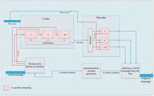
The coder block takes 128 bits of information from the buffer to encrypt the data. Coder consists of 10 parallel coder16. A maximum input data size for a coder16 subblock is 16 bits. Therefore, it is necessary to divide input data into 10 parts. The 10 subblocks are formed by generating pseudorandom numbers. The pseudorandom number generator generates 10 random numbers, and the sum of all numbers must be 128. Generation of pseudo-random numbers is done by a shift register algorithm with linear feedback. The program code of the shift register algorithm with linear feedback was written in Verilog:
module lfsr(
input rst,
input clk,
input enable,
input [3:0] taps,
output [3:0] out,
);reg [3:0] shift_reg;
assign out = shift_reg;
wire next_bit;
assign next_bit = shift_reg(Shan`gin, Citation2007) ^ shift_reg[0];
always @(posedgeclk)
if (rst)
shift_reg≤ taps;
else
if (enable)
shift_reg≤ {next_bit, shift_reg[3:1]};
endmodule
The shift register algorithm consists of an XOR logic element and a shift register. The shift register algorithm with linear feedback can generate numbers from 1 to 15 and can repeat after 15 reports. The numbers are not repeated in the same report. For example, 1, 8, 4, 2, 9, 12, 6, 11, 5,10, 13, 14, 15, 7, 3, but the sum of 10 random numbers will not always be 128. Therefore, it is necessary to change the range of random numbers by taking modulo 6 and adding 11. As a result, 9 numbers are generated randomly from a range of 11 to 16, and the tenth from the difference of 128 from the sum of the previous numbers.
The encryption keys and base systems
for the different bits were generated using the software part of the cryptosystems. The software code for data encryption was written in Verilog according to the formula:
where,
- source data,
- encryption key,
—base system. The process of encryption in 10 subblocks is performed in parallel. After encryption, data from each subblock is connected in a cascading manner, and as a result, we obtain L(x) data with a size of 160 bits.
Listing of the program code for selecting the encryption key and the base system:
begin
case (N)
4: begin B ≤ 16`o6; P ≤ 17`o31: end
5: begin B ≤ 16`o37; P ≤ 17`o45: end
6: begin B ≤ 16`o57; P ≤ 17`o103: end
7: begin B ≤ 16`o147; P ≤ 17`o217: end
8: begin B ≤ 16`o355; P ≤ 17`o453: end
9: begin B ≤ 16`o763; P ≤ 17`o1003: end
10: begin B ≤ 16`o1117; P ≤ 17`o2011: end
11: begin B ≤ 16`o3511; P ≤ 17`o4053: end
12: begin B ≤ 16`o5171; P ≤ 17`o10011: end
13: begin B ≤ 16`o10063; P ≤ 17`o20033: end
14: begin B ≤ 16`o35613; P ≤ 17`o40041: end
15: begin B ≤ 16`o76203; P ≤ 17`o10003: end
16: begin B ≤ 16`o161201; P ≤ 17`o20053: end
endcase
end
The decoder unit divides 160 bits of encrypted data into 16 bits and decrypts a data in parallel. During decryption, inverse keys and base systems for different bits are generated using software section of the cryptosystem. When decrypting data, we get ten 16-bit subblocks. We need to cut out the necessary part and get the initial data of 128 bits in size. The decoder block has a pseudo-random number generation subblock, which repeats the number sequence of the division of the 128-bit input data according to encryption. As a result we get initial information. The snippet of the program code of the decoding block with the function of division of 160 bits by 16 bits:
always @ (posedgeclk)
begin
in_info (Shan`gin, Citation2007) ≤ {1`b0, info [159:144]};
in_info (Saini et al., Citation2020) ≤ {1`b0, info [143:128]};
in_info (RyabkoB & Fionov, Citation2004) ≤ {1`b0, info [127:112]};
in_info (Barrera et al., Citation2020) ≤ {1`b0, info [111:96]};
in_info (Aitkhozhayeva & Tynymbayev, Citation2014) ≤ {1`b0, info [95:80]};
in_info (Gnatyuk et al., Citation2016) ≤ {1`b0, info [79:64]};
in_info (Tenca & Tawalbeh, Citation2003) ≤ {1`b0, info [63:48]};
in_info (Nedjah & de Macedomourelle, Citation2006) ≤ {1`b0, info [47:32]};
in_info (Sadiq & Ahmed, Citation2006) ≤ {1`b0, info [31:16]};
in_info (Zambreno et al., Citation2006) ≤ {1`b0, info [15:0]};
end
decoder16 decoderN1(
.A (in_info (Shan`gin, Citation2007)),
.clk (clk),
.N (rand (Shan`gin, Citation2007)),
.out (out_decoder (Shan`gin, Citation2007)));
3. Results and discussion
The results of data encryption and decryption are shown in as a timeline diagram. In , the data subject to encryption, which are distributed in blocks randomly, is fed to the info input: 12, 13, 15, 13, 14, 11, 11, 16, 16, 7 (the lengths of subblocks of the initial 128-bit ciphertext). Also, unique irreducible polynomials and direct keys are randomly fixed in these blocks, which take part in multiplication of input data polynomials, keys modulo irreducible polynomials. As can be seen in , the output of coder_info forms an encrypted value: 0d891ef43f1a19ba127306ca00c40bc632ca0036 in hexadecimal notation.
Figure 4. The timeline diagram of encryption and decryption for a different sequence of numbers separating an original information
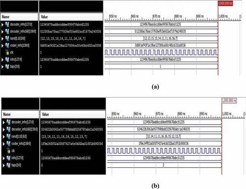
Changing lengths of the subblocks in an initial 128-bit ciphertext in random order (13, 14, 11, 11, 16, 16, 15, 12, 13, 7), we get coder_info output in hexadecimal notation: 1f9e24ff02a005f7427a4c0d32ba01ff1b590036 (). In both cases, we get a decrypted ciphertext at the output of decoder_info.
A visualization block consists of three sub-blocks: synchronous signal formation with a certain frequency, the driver for VGA and symbol formation for displaying on a screen ().
Figure 5. Block of information visualization on the display
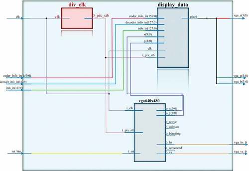
VGA driver block generates synchronous signals according to the vertical and horizontal position of a monitor. The block has inputs coder_info_in, decoder_info_in and info_in, which correspond to encrypted, decrypted and raw data.
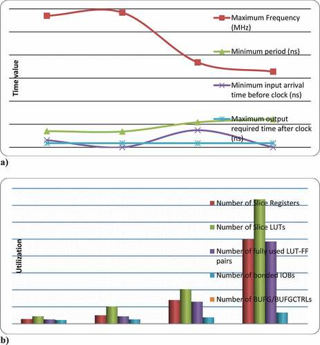
The encryption algorithm was implemented on a Nexys 4 DDR development board with an Artix-7 FPGA core (XC7A100T-1CSG324C) from Xilinx. The device has been selected for its optimum performance, which one is suitable for the job. shows the number of slice registers, the number of LUTs of slices, the number of fully usable LUT-FF pairs, the number of IOBs linked, the number of RAM/FIFO blocks, the number of BUFG/BUFGCTRL, etc. necessary in the design of the microcircuit. also includes the details of the parameters related to time synchronization, such as details of the maximum frequency, minimum period, minimum time required before CLK, maximum time after CLK.
Table 1. Hardware parameters summary as FPGA synthesis report
Table 2. Timing summary as FPGA synthesis report
The proposed FPGA-based data encryption and decryption algorithm was compared with other data analyses of the cryptographic algorithm implemented on the FPGA hardware. This algorithm is shown in the article by Niraj Kumar et al. (A. Kumar et al., Citation2019; Niraj Kumar et al., Citation2021).
show timing and used hardware resource when encrypting data of various sizes. The use of equipment resources increases as length of the encryption block increases, except for used memory, since the calculation is performed iteratively for the n-bit. A larger key size increases the number of conversion cycles for the designed encryption and decryption chip, which increases the combinational path delay, minimum and maximum timing pulse synchronization. The performance of the microcircuit is estimated based on the maximum frequency supported by the FPGA hardware.
Figure 6. (a) Timing summary as FPGA synthesis report (b) Using the FPGA hardware resource
The results of this work can be used at developing an embedded encryption block for modern stand-alone digital devices.
With hardware implementation of such blocks as polynomial irreducibility checking, direct and inverse key generators, as well as high-performanc ьe polynomial multipliers on matrix-conveyor circuits, etc., high-speed devices for data encryption can be built.
4. Conclusion
The encryption device was developed and tested using NPN based FPGA. In the process of implementation of this device were applied methods of multithreaded parallel computation with the formation of information modules based on a random number generator. This encryption method not only speeds up the entire process, but also increases a cryptographic strength of ciphertext.
The developed FPGA-based encryption device for high-speed data encryption can be embedded into an architecture of a personal computer. It is possible to build autonomous high-performance encryption digital devices with hardware implementation of a set of irreducible polynomials and autonomous generation of keys and implementations of encryption block with conveyor organization
Author contributions
Drawing up a circuit model of the device: T.S., S.A.; FPGA design and programming: I.M., K.Y., Zh.D.; writing—review and editing: T.S., I.M., S.A., K.Y., Zh.D.; All authors have read and agreed to the published version of the manuscript.
Acknowledgements
The authors thank the outstanding work of the Committee of Science of the Ministry of Education and Science of the Republic of Kazakhstan.
Disclosure statement
No potential conflict of interest was reported by the authors.
Additional information
Funding
Notes on contributors
A.A. Skabylov
Skabylov Alisher Aliuly – received the B.S. degree in Radio engineering, Electronics, and Telecommunications and M.S. degree Information Systems from Al-Farabi Kazakh National University, Almaty, Kazakhstan, in 2015 and 2017, respectively. He is currently pursuing the Ph.D. degree in the Department of Physics and Technology at Al-Farabi Kazakh National University, Almaty, Kazakhstan. eacher of the Department of Solid State Physics and Nonlinear Physics of Al-Farabi Kazakh National University. The main research interests of Skabylov A. A. are related to the method of information protection, and the implementation of digital devices and information protection systems based on programmable logic integrated circuits.
References
- Aitkhozhayeva, Y., & Tynymbayev, S. (2014). Aspects of hardware modulation in asymmetric cryptography. Journal Vestnik NAS RK, 5, 88–14. ISSN-. https://www.kaznu.kz/content/files/pages/folder23401/%D0%92%D0%B5%D1%81%D1%82%D0%BD%D0%B8%D0%BA_05_2014_%D0%9D%D0%90%D0%9D%D0%A0%D0%9A.pdf#page=88
- Barrera, A., Cheng, C.-W., & Kumar, S. (2020, June 24–26). A fast implementation of the Rijndael substitution box for cryptographic AES. In Proceedings - 2020 3rd international conference on data intelligence and security (Vol. 9323014, pp. 20–25). South Padre Island, TX: IEEE. https://doi.org/10.1109/icdis50059.2020.00009
- Gnatyuk, S., Okhrimenko, A., Kovtun, M., Gancarczyk, T.,&Karpinskyi, V. (2016, October 16–19). Method of algorithm building for modular reducing by irreducible polynomial. In Proceedings of the 16th international conference on control, automation and systems (pp. 1476–1479). Gyeongju, Korea (South): IEEE. https://doi.org/10.1109/iccas.2016.7832498
- Kalimoldayev,M., Tynymbayev,S., Gnatyuk,S., Ibraimov,M.,&Magzom,M.(2020). The device for multiplying polynomials modulo an irreducible polynomial. News of the National Academy of Sciences of the Republic of Kazakhstan Series of Geology and Technical Sciences, 2(434), 199–205. https://doi.org/10.32014/2020.2518-170X.60
- Kalimoldayev, M., Tynymbayev, S., Gnatyuk, S., Magzom, M., Khokhlov, S., & Kozhagulov, Y. (2020). Matrix multiplier of polynomials modulo analysis starting with the lower order digits of the multiplier NEWS of the Academy of Sciences of the Republic of Kazakhstan Series of Geology and Technical Sciences. News of the National Academy of Sciences of the Republic of Kazakhstan, 4(436), 181–187. https://doi.org/10.32014/2019.2518-170X.113
- Kalimoldayev, M., Tynymbayev, S., Magzom, M., Ibraimov, M., Khokhlov, S., Abisheva, A., & Sydorenko, V. (2019, June 12). Polynomials multiplier under irreducible polynomial module for highperformance cryptographic hardware tools. In CEUR workshop proceedings. 15th international conference on ICT in education, research and industrial applications. Integration, harmonization and knowledge transfer, ICTERI 2019 (Vol. 2393, pp.729–737). Kherson.
- Krishna, B. M., Khan, H., Madhumati, G. L., Kumar, K. P., Tejaswini, G., Srikanth, M., & Ravali, P. (2017). FPGA implementation of DES algorithm using DNA cryptography. Journal of Theoretical and Applied Information Technology, 95(10), 2147–2158. https://www.scopus.com/record/display.uri?eid=2-s2.0-85020191255&origin=resultslist&sort=plf-f&src=s&sid=8091300ea67e316acead5bc399fd321d&sot=b&sdt=b&sl=75&s=TITLE-ABS-KEY%28FPGA+implementation+of+DES+algorithm+using+DNA+cryptography.%29&relpos=0&citeCnt=3&searchTerm=
- Kumar, A., Vishnoi, P., & Shimi, S. L. (2019). Smart grid security with cryptographic chip integration. EAI Endorsed Transactions on Energy Web, 19(23), 6. https://doi.org/10.4108/eai.13-7-2018.157037
- Kumar, N., Mishra, V. M., & Kumar, A. (2021). Smart grid and nuclear power plant security by integrating cryptographic hardware chip. Nuclear Engineering and Technology, 53(10), 3327–3334. https://doi.org/10.1016/j.net.2021.05.006
- Liu, W., Fan, S., Khalid, A., Rafferty, C., & O’Neill, M. (2019). Optimized schoolbook polynomial multiplication for compact lattice-based cryptography on FPGA. In IEEE transactions on Very Large Scale Integration (VLSI) systems (Vol. 27(10), pp. 2459–2463). Institute of Electrical and Electronics Engineers Inc. https://doi.org/10.1109/tvlsi.2019.2922999
- Nedjah, N., & de Macedomourelle, L. (2006). A review of modular multiplication methods and respective hardware implementations. Informatica, 30(1), 111–129 https://www.scopus.com/record/display.uri?eid=2-s2.0-33244487252&origin=resultslist&sort=plf-f&src=s&sid=14e19744d3164b83e97af2029c0edc5e&sot=b&sdt=b&sl=97&s=TITLE-ABS-KEY%28A+review+of+modular+multiplication+methods+and+respective+hardware+implementations%29&relpos=0&citeCnt=37&searchTerm=.
- RyabkoB, Y., & Fionov, A. I. (2004). Osnovy sovremennoy kriptografii dlya specialistov v informacionnyh technologiyah. Nauchnyi Mir, 173 s (in Russ.).
- Sadiq, M., & Ahmed, J. (2006). Complexity analysis of multiplication of long integers. Asian Journal of Information Technology, 5(2), 111–112. https://doi.org/10.1109/sbcci.2002.1137629
- Saini, R., Jain, M., & Suneja, K. (2020). FPGA Based Design of Speech Encryption and Decryption for Secure Communication. Communications in Computer and Information Science, 1170, 37–49. ISSN: . https://doi.org/10.1007/978-981-15-9671-1_3
- Shan`gin, V. E. (2007). Zashitainformacii v kompiuternyhsistemahisetyah. DMK Press. 592 s. (in Russ).
- Tenca, A. F., & Tawalbeh, L. A. (2003). Algorithm for Unified Modular Division in GF(p) and GF(2n) Suitable for Cryptographic Hardware. Electronics Letters, 40(5), 304–306. https://doi.org/10.1049/el:20040233
- Wollinger, T., Guajardo, J., & Paar, C. (2004). Cryptography on FPGAs: State of the art implementations and attacks, In Special issue on embedded systems and security of the ACM Transactions in Embedded Computing Systems (TECS) (Vol. 3). ACM Transactions on Embedded Computing Systems. https://doi.org/10.1145/1015047.1015052
- Zambreno, J., Honbo, D., Choudhary, A., Simha, R., & Narahari, B. (2006). High performance software protection using reconfigurable architectures. In Proceedings of the IEEE (Vol. 94( 2)). IEEE. https://doi.org/10.1109/jproc.2005.862474