
 ?Mathematical formulae have been encoded as MathML and are displayed in this HTML version using MathJax in order to improve their display. Uncheck the box to turn MathJax off. This feature requires Javascript. Click on a formula to zoom.
Abstract
In this study, the front work function WFITO and absorber layer bandgap’s influences on two solar cells structure performances, namely ITO/(p)a-Si:H/(i)a-Si:H/(n)a-Si:H/metal (single intrinsic, Sint) structure and ITO/(p)a-Si:H/(i1)a-Si:H/(i2)a-Si:H/(n)a-Si:H/metal (double intrinsic, Dint) structure, fabricated using RF-PECVD method were simulated, using AFORS-HET (Automated FOR Simulation of Heterostructures) software. Based on these simulations, the work functions (WFITO) value ought to range from 4.9 to 5.7 eV, in order to determine the optimum WFITO for high solar cell efficiency, confirmed with the J-V dark characteristic, the band diagram in thermodynamics equilibrium, build-in electric field distribution, trapped holes density, as well as the quantum efficiency. The simulation results showed the Dint structure’s external parameters (e.g., VOC,JSC, FF, Eff) are higher, compared to the Sint structure. Furthermore, the absorber (i1 and i2) layers bandgap is optimized in an effort to improve the Dint solar cell’s performance. According to the results, the Dint structure had a 10.76 % maximum efficiency (VOC = 969.8 mV, JSC = 16.03 mA/cm2, and FF = 70 %), using WFITO, i1 layer bandgap, and i2 layer bandgap of 5.7 eV, 1.82 eV, and 1.86 eV, respectively.
PUBLIC INTEREST STATEMENT
Hydrogenated amorphous silicon-based solar cells (a-Si:H) have several advantages to be developed as inexpensive, non-toxic, and environmentally friendly solar cells. In this study, optimization efforts were carried out to increase the conversion efficiency through simulation of the (p-i-n)a-Si:H structure solar cells fabricated using RF-PECVD realized by our research group. Modification of the work function at the ITO/(p)a-Si:H interface and the addition of intrinsic layers with different band gap values resulted in a new structure (p-i1-i2-n)a-Si:H which has been shown to increase the conversion efficiency, both based on experimental and simulation results. Furthermore, the simulation results are compared with the simulation results of other similar thin-film solar cells. The results showed that the structural modification using the work function value at the appropriate ITO/(p)a-Si:H interface and the addition of an intrinsic layer on the (p-i-n)a-Si:H structure resulted in higher VOC values and good conversion efficiency. The proposed structure of the (p-i1-i2-n) solar cells provides a reference for further development in solar cells technology.
1. Introduction
Hydrogenated amorphous silicon (a-Si:H) is a semiconducting material explored in the last three decades, due to its potential application in thin-film solar cell development. Green et al, Citation2021, reported a-Si:H single-junction based solar cells have a low efficiency of about 10.2% (Green et al., Citation2021), due to several limitations, including parasitic optical absorption in doped layers, defects at p/i and i/n interfaces, lower optical absorption in the absorber layer, and limited light trapping within the cells (Shin et al., Citation2017). Therefore, one of the main issues to increase the a-Si: H solar cell’s efficiency is to improve the quality a-Si:H layers. The intrinsic layers (i-a-Si:H) must have good electrical transport, in order to sustain photogeneration for holes and electrons to exit the device before recombination. In addition, this layer must have a suitable ability to absorb light and consequently, generate more electron-hole (e-h) pairs (Son et al., Citation2018). According to a previous study, adding an active layer with a different bandgap in the p-i-n layer with an optimum thickness in order to maintain material quality improved the solar cell’s efficiency from 5.61 % (p-i-n type) to 8.86 % (p-i1-i2-n type; Prayogi et al., Citation2021). The TCO’s work function also strongly influences the cell’s performance (Belfar, Citation2015). Thus, quality TCO/(p)a-Si:H contact, as well as Ohmic contact, is achievable through increased TCO work function, in order to minimized the band offset, and consequently, reduce the device’s electron injection barrier height (Y. S. Park et al., Citation2013).
The energy band offset between semiconductor and TCO ought to be minimized, in order to improve ohmic contact. Therefore, inserted transparent conductive oxides (for instance, Indium Tin Oxide, ITO) with high conductivity (σ > 103 S/cm), good transparency in the visible range (T > 90 %), and higher work function values are required for the higher possibility to carrier injection into TCO/(p)a-Si:H interface. For thin film solar cells, a work function of TCO associated with carrier injection into TCO/(p)-window interface which influences plays a dominant role in the device parameters such as VOC and FF (Oh et al., Citation2012; Rached & Mostefaoui, Citation2008). The deposition of ITO films on Corning 1737 substrate, using RF-Magnetron Sputtering method improved ITO work function from 4.67 to 5.66 eV, by the O2 plasma treatment and an almost stable resistivity (J. Park et al., Citation2013). Meanwhile, the electrical and optical characteristics of the ITO films are improved by doping the films with high permittivity materials (Zr, ZrO2), and this results in high mobility and work functions due to the excellent surface (Hussain et al., Citation2014; Khokhar et al., Citation2020; Zhang, Citation2010). Furthermore, optical losses in TCO were reduced without compromising with Rs and recombination loss, using ITO/SiOx stacks, to produce the short circuit current density (JSC) > 41.3 mA/cm2, with a 100 Ω sheet resistance, while ITO/SiNx/SiOx produced a 42 mA/cm2 JSC, with a 300 Ω sheet resistance (Herasimenka et al., Citation2016). Cruz et al., also reported the effect of various TCO (ITO, ZnO:Al, IO:H) as rear-junction of the silicon heterojunction solar cells, through experiments and simulation (Cruz et al., Citation2019).
In this study, the effect of changes in work function (WFITO) of the ITO/p-layer interface, on the single intrinsic layer, Sint (p-i-n type) and double intrinsic layer, Dint (p-i1-i2-n type) solar cell performances were simulated using AFORS-HET software. The band diagrams, J-V characteristics, electrical field distribution, trapped holes density, and quantum efficiency were also simulated, to further understand the solar cells’ high performances. In addition, the optimum absorber layer bandgaps’ influence in improving the Dint structure’s optical and electrical output was investigated.
2. Simulation methods
2.1. Physical model
This study used well-practiced AFORS-HET to accurately evaluate the effect of numerous parameters on the solar cell’s performances. This software solves the 1-D Poisson´s equation and the continuity equation for electrons as well as holes, using Shockley–Read–Hall (SRH) recombination statistics. Also, e-h pair generation in the absorber layer is estimated with the Beer–Lambert absorption equation, using the optical model in AFORS-HET. The detailed equation used in AFORS-HET is expressed in (Stangl, Citation2010).
where is the absolute dielectric constant,
is the electric potential,
is the electron charge,
and
are electrons and holes densities,
and
are the doping densities (donor and acceptor) at the fixed position
,
is the defect density of charge defect specifying the number of traps at any energy position E within band gap (the defect type can be empty or occupied with a single or double electron),
denotes the generation rate for carriers,
is the recombination rate, respectively.
Furthermore, localized state density describing layers a-Si:H is expressed as exponential band tail defect states (Urbach tails) and Gaussian mid-gap states (dangling bond) is expressed in (Stangl, Citation2010).
where and
are the tail state density per energy range at the conduction and valence bands,
and
are characteristic decay energy (Urbach energy) of the conduction and valence bands, EV and EC are the valence and conduction band energies,
is total dangling bond state density,
is specific energy of Gaussian dangling bond peak, and
is standard deviation of the Gaussian dangling bond distribution.
2.2. Devices structures and input parameters
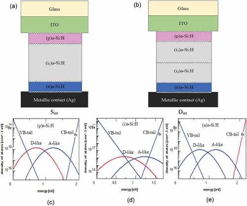
In this study, the Sint and Dint hydrogenated amorphous silicon solar cell structures were fabricated by our research group, fabricated using RF-PECVD (MVSystem Inc., USA), as shown in . Meanwhile, ) shows the simulation details, ITO/(p)a-Si:H(15 nm)/(i)a-Si:H(600 nm)/(n)a-Si:H(25 nm)/metal (Sint), and ITO/(p)a-Si:H(15 nm)/(i1)a-Si:H(300 nm)/(i2)a-Si:H(300 nm)/(n)a-Si:H(25 nm)/metal (Dint). Meanwhile, the solar cell’s second structure was fabricated with the (i)a-Si:H split into two parts, (i1)a-Si:H (300 nm and Eg = 1.70 eV) as well as (i2)a-Si:H (300 nm and Eg = 1.85 eV). The structure detailed fabrication was carried out as described by (Prayogi et al., Citation2021). ) shows the (p)a-Si:H (i)a-Si:H, and (n)a-Si:H layers’ gap states distribution, described as exponential band tail defect states and Gaussian mid-gap states (dangling bond states).
Figure 1. Prototypes of p-i-n and p-i1-i2-n based amorphous silicon solar cell’s fabricated using RF-PECVD reactor realized in our research group.
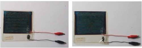
Figure 2. Schematic of (a) single intrinsic (Sint) structure, (b) double intrinsic (Dint) structure, (c-e) the DOS for different types of the a-Si:H produced by AFORS-HET simulator. D-like and A-like declares donor like and acceptor like Gaussian mid-gap states, VB-tail and CB-tail declares valence band and conduction band, respectively.
The effects of WFITO at ITO/(p)a-Si:H interface on the Sint and Dint solar cell devices’ performances were observed numerically using AFORS-HET, however, this was not studied by Prayogi, et al. In addition, the absorber (i1,i2) layers’ bandgap was optimized for improved Dint solar cell performance. The radiation AM1.5 G spectrum with 100 mW/cm2 power density was used as illuminating source, while the operational temperature was 300 K. Meanwhile, for parameters input simulation, the surface recombination velocity (Sit) of the front as well as back contact was assumed to be both 1.0 × 107 cm/s. The barrier height at front contact (ITO/(p)a-Si:H layer) was taken to the calculation by changing the WFITO, while the barrier height at back contact
((n)a-Si:H layer/metal) was kept constant 0.2 eV. Also, the front contact was assumed to reflect (RF) 10 % of the incident light, while the back counterpart was assumed to be 0 or no back reflector (RB). The p-window and n layers’ mobility bandgap were set to be 2.0 eV and 2.2 eV, respectively, while the absorber layers (i1 and i2) counterpart ranged from 1.7 to 1.86 eV. shows the typical parameters used in the simulations in more detail, as described in previous studies (Belfar, Citation2015; Hernández-Como & Morales-Acevedo, Citation2010; Prayogi et al., Citation2021).
Table 1. Parameters input for simulation of the solar cells using AFORS-HET
3. Simulation results and discussion
3.1. Influences of WFITO on the performances of the solar cells
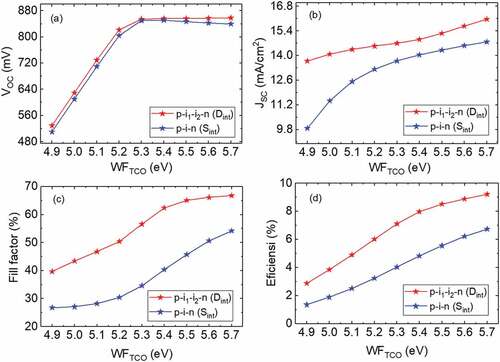
In this simulation, the ITO work function’s values were varied between 4.9 to 5.7 eV, according to experimental results deposited by RF sputtering, depending on deposition conditions (Kim et al., Citation2009; Klein et al., Citation2010; Y. S. Park et al., Citation2013). illustrates the Sint and Dint solar cells simulated electrical parameters as a function of WFITO using AFORS-HET, in order to determine the optimum WFITO for high solar cell efficiency. According to ), the VOC values increased with increase in WFITO from 4.9 to 5.3 eV for both structures, due to shift of the front contact barrier (reduction in the band bending), with a direct influence on increasing built-in potential,
, as shown in expression (Belfar, Citation2015; Jensen et al., Citation2002).
Figure 3. Simulated electrical parameters of the Sint and Dint solar cell structures as a function of WFITO (a) open circuit voltage (VOC), (b) current density (JSC), (c) fill factor (FF), and (d) the conversion efficiency (Eff).
where is the electron affinity of p-window layer,
is the barrier height at back contact,
is diode ideality factor,
is the thermal energy,
is the effective density of states in the valence band,
is the interface recombination velocity. From Equationeq. (7)
(7)
(7) -(Equation8
(8)
(8) ), it is clear that the Vbi has a larger value when WFITO is higher and the VOC increases with the built-in potential. However, when WFITO = 5.7 eV, the built-in potential Vbi = 1.7 eV which is enough to effectively separate the carriers and provides the strong electrical field, resulting in a high value of VOC.
) shows the current density values JSC for both structures were observed to increase with change in WFITO, consequently, improving photogenerated hole passage from the p-window to ITO layer. According to ), as the WFITO increases, the two structures’ FF values also increased, due to migration of holes from the p-window layer to the ITO interface, with reduction in the surface band bending the hole injection barrier (Oh et al., Citation2012). Meanwhile, ) shows the Sint and Dint structure’s maximum efficiency is about 6.73 % (VOC = 839.4 mV, JSC = 14.78 mA/cm2, and FF = 54.25 %) and 9.21% (VOC = 858.1 mV, JSC = 16.07 mA/cm2, and FF = 66.80 %), respectively, at WFITO = 5.7 eV. Low FF values from the simulation result is following with the experimental results reported by (Park et al., Citation2012). This is presumably for both structures, due to the imperfect joint formation mechanism creating defect conditions at the ITO/p-window layer interface.
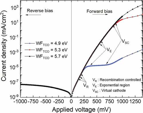
As previously mentioned, the Dint solar cell structure has a better performance, compared to the Sint solar cell structure, and is therefore to be the focus of the discussion. The correlation between the behavior of solar cells in the dark and the WFITO value will be analyzed to test the quality of the solar cells with electrical parameters in the dark (dark parameters), namely the reverse saturation current, J0. shows the J-V characteristics under dark for typical WFITO of 4.9 eV, 5.3 eV, and 5.7 eV, applied to Dint structure. In reverse bias, the J0 is not typically dependent on the WFITO and the J0 values at Vapp = −1000 mV were about 5.39 × 10⁻⁸ mA/cm2 (WFITO = 4.9 eV), 5.29 × 10⁻⁸ mA/cm2 (WFITO = 5.3 eV), and 5.26 × 10⁻⁸ mA/cm2 (WFITO = 5.7 eV), respectively. Conversely, the dark current’s value in forward bias is influenced by WFITO. also shows the dark current is entirely controlled by recombination of e-h pairs through mid-gap states within the absorber layer (VR region), at low forward bias (< 250 mV). Meanwhile, for voltage inside the exponential region (VE), the dark current is limited by the combination of diffusion and recombination. However, for the region between VR < V < VE (250 < V < 400 mV), the dark current trundles, terraces more slowly with voltage, and is fully controlled by electron diffusion around virtual cathode. This region is the space charge limited current (SCLC) in region V > VSC, as a function concentration of trapped electrons and holes (Sturiale et al., Citation2009). For forward bias V > 400 mV, the forward dark current increases significantly and is controlled by hole injection at the ITO/p-window layer interface (Belfar, Citation2015).
Figure 4. Simulated the J-V characteristic of the Dint solar cell structure under dark for typical WFITO = 4.9 eV, 5.3 eV, and 5.7 eV.
A study by Prayogi et al., (Citation2021) reported the fabrication of Dint solar cell with RF-PECVD, using SiH4 (10 % concentration in H2 gas), B2H6 (10 % concentration in H2 gas) for dopant source of the p-type layer, and PH3 (10 % concentration in H2 gas) for dopant source of the n-type layer gases mixture. The presence of hydrogen in a-Si:H film plays a role in filling localized states to degrade defect states. However, the excess hydrogen traced after filling localized states in the absorber layer tends to become an impurity. Consequently, the JSC is reduced by the defects generated by hydrogen impurity (J. Park et al., Citation2013).
shows the Dint’s band diagram simulation generated using AFOSR-HET simulator for typical WFITO. An increase in WFITO requires an increase in the front contact barrier and a significant decrease in the downward band bending
emerges at the ITO/p-window layer leading to improvement of VOC, as shown in EquationEquations. (7)
(7)
(7) -(Equation8
(8)
(8) ). Simultaneously, the FF values were increased due to the migration of holes to the front contact ITO/p-window layer interface, as the hole injection barrier,
was reduced (Oh et al., Citation2012). shows the AFORS-HET simulation results from the Dint solar cell performances with different WFITO. The high WFITO of 5.7 eV produced a 9.21 % maximum efficiency in the Dint solar cell, due to the enhanced VOC and FF, as shown in expression (Bechane et al., Citation2021; Singh et al., Citation2012; Sultana et al., Citation2017).
Figure 5. Simulated band diagram of the p-i1-i2-n solar cell generated by AFORS-HET for typical WFITO = 4.9 eV, 5.3 eV, and 5.7 eV.
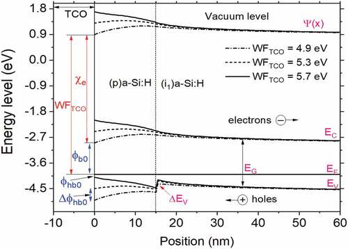
Table 2. AFORS-HET simulation results for the Dint solar cell performances with different the WFITO
where ,
are the photogenerated current, the reverse saturation current, the elementary charge, the terminal voltage, the ideality factor, and thermal energy, the normalized
and
is power density of light entering the cell, respectively. According to the EquationEquations. (9)
(9)
(9) -(Equation11
(11)
(11) ), the open circuit voltage VOC terrace with the photogenerated current (
). It is clear from , that maximum value of the VOC and FF are 858.1 mV and 66.8 % for WFITO = 5.7 eV. At the same time, the efficiency enhancement is due to increases in the VOC and FF values.
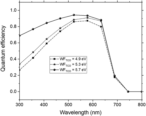
However, the WFITO’s influence on optical properties and photogenerated current were examined for light spectrum at 300–800 nm. The AFORS-HET simulated results of the p-i1-i2-n solar cell’s quantum efficiency indicate a WFITO of 5.7 eV is able to improve in blue light response between 300 and 633 nm, with a maximum quantum efficiency of 94.3 % at 522 nm (). The photogenerated current () value can be written as (Belfar, Citation2015).
Figure 6. Simulated quantum efficiency of Dint solar cell for typically WFITO = 4.9 eV, 5.3 eV, and 5.7 eV which examined for the range of the light spectrum of 300–800 nm.
where is the photon flux incident on the solar cell at wavelength
,
is the reflection coefficient from the top surface;
is the quantum efficiency. From Equationeq. (12
(12)
(12) ), it is obvious that with high value of WFITO,
and
(
) of Dint solar cell are significantly improved, as shown in .
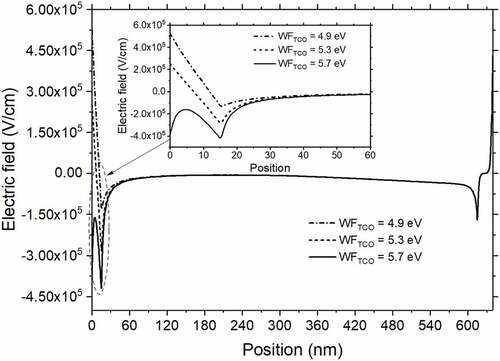
Furthermore, the changes in with WFITO are due to alteration of the electric field at ITO/p-window layer interface, caused by different carrier concentrations, leading to a significant reduction in J0, and consequently, improving the VOC. Based on , an increase in WFITO from 4.9 eV to 5.3 eV, results in a change in the electric field from +5.23 x 10⁵ to +2.51 x 10⁵ Vcm−1 at ITO/p-window layer interface, and this impedes the photogenerated hole from reaching the front contact. Meanwhile, at a WFITO of 5.7 eV, the electric field’s value shifted to negative (−3.89 x 10⁵ Vcm−1), thus, providing effective forces for holes transport to reach the front contact.
Figure 7. Simulated electric field distribution of the Dint solar cell for typical WFITO = 4.9 eV, 5.3 eV, and 5.7 eV. (inset) the electric field profiles at the (p)a-Si:H-window layer/(i1)a-Si:H interface.
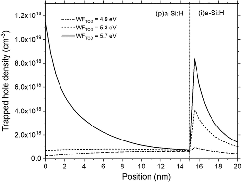
As mentioned above, reduction of the associated with the barrier of the ITO/p- layer Schottky contact is lessened even to be negligible with high value ITO work function (WFITO). Consequently, the quantity of photogenerated holes more collect at front contact as trapped holes density (Kumar & Ranjan, Citation2020). shows that the trapped holes concentration at ITO/p-window layer increased to 1.14 × 1019 cm−3 for the highest WFITO of 5.7 eV, as compared to 7.14 × 1017 cm−3 and 2.38 × 1017 cm−3 for lower WFITO of 5.3 eV and 4.9 eV, respectively. However, for silicon thin film solar cells a change in the work function of ITO films (WFTCO) is associated with a change of the front barrier height (
) affects to the efficiency of carrier injection into TCO/(p)a-Si:H interface.
Figure 8. Simulated the trapped holes density the Dint solar cell for typical WFITO = 4.9 eV, 5.3 eV, and 5.7 eV.
3.2. Optimization results of the a-Si:H absorber layers
According to Benigno and Darminto, p-i-n a-Si:H based solar cell fabrication using RF-PECVD technique, by varying the hydrogen dilution () = 0, 16, 36 for intrinsic (absorber) layers with 600 nm optimum thickness, inserted between p-type and n-type layers, has been conducted, and a 5.78% maximum efficiency was achieved (Benigno & Darminto, Citation2017). Prayogi et al., reported an effort to enhance the p-i-n solar cell’s performance through modification by adding the intrinsic layer (i2) with different hydrogen dilution to the original Sint structure produced a Dint solar cell structure with good optical properties, as well as an 8.61% maximum efficiency (Prayogi et al., Citation2021). The i1-i2 layers serial structure leads to a more excitonic (e-h pairs) state because the i1 (= 1.70 eV) and i2 (= 1.85 eV) layer bandgaps are different.
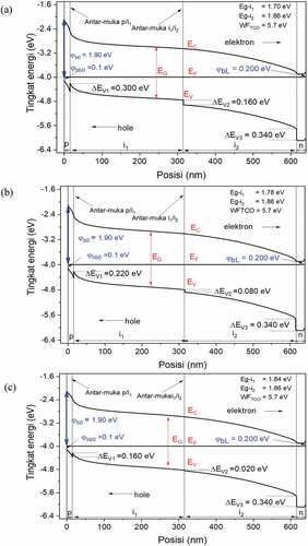
) shows the optimized results of the i1 and i2 layer bandgap variations, in order to improve the p-i1-i2-n solar cell’s performance. During the absorber layers’ optimization, the (p)a-Si:H and (n)a-Si:H layers bandgap values were taken to be 2.0 and 2.2 eV, respectively. Meanwhile, the (p)a-Si:H, (i1)a-S:H, (i2)a-Si:H, and (n)a-Si:H films’ thicknesses were 15 nm, 300 nm, 300 nm, and 25 nm, respectively. In this case, the WFITO value as neutral contact at ITO/p-window layer was also taken to be 5.7 eV. Based on ) shows the VOC values gradually increased from 858.1 to 1007 mV in the bandgap range of 1.70 to 1.86 eV, and this confirmed the p-i1-i2-n solar cell’s band diagram structures ()). Furthermore, the bandgap offsets () emerges in each junction at valence band, due to the bandgap difference between the p-i1, i1-i2, and i2-n layers, and this offset (discontinuity) is able to increase the recombination rate and trapped hole density at those interfaces, consequently, leading to low VOC ()). According to , a change in the i1 bandgap change to 1.78 eV and 1.84 eV, led to a decline in the
within the p-i1 and i1-i2 valence band, associated with high VOC. However, with a change in the i2 layer band gap 1.70 to 1.78 eV, the i1 layer bandgap remained 1.82 eV, and the VOC values remained constant at 1004.4 mV, but slowly increased with changes in the i2 layer bandgap ()).
Figure 9. The external parameter results of (a) i1-layer bandgap, (b) i2-layer bandgap variations of the Dint solar cell.
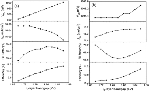
Figure 10. Simulated band diagram of the Dint structure with different of the i1 and i2 bandgaps which valence band offsets were appeared at p/i1, i1/i2, and i2/n interfaces. (a) Eg-i1 = 1.70 eV, Eg-i2 = 1.86 eV, (b) Eg-i1 = 1.78 eV, Eg-i2 = 1.86 eV, (c) Eg-i1 = 1.84 eV, Eg-i2 = 1.86 eV.
Based on ), the JSC values were discovered to be constant in the bandgap range of 1.70 to 1.74 eV, but were observed to drastically dwindle from 16.08 to 15.98 mA/cm2, with a change in the i1 bandgap from 1.74 to 1.86 eV, due to less generation of excitonic in absorber layers with increase in the i1 bandgaps. Meanwhile, the i2 bandgap (Eg-i1 = 1.82 eV) change from 1.7 to 1.86 eV did not cause any significant change ()). VOC increased with the i1 layer bandgap, from 1.70 to 1.80 eV, as well with the variations of FF, from 66.80 % to 69.12 %. FF also slightly declines for the i1 layer bandgap > 1.80 eV. Conversely, the reduction in FF from 70.27 % to 67.10 % was associated with changes in the i2-layer bandgap from 1.70 to 1.82 eV. However, beyond 1.82 eV, FF was observed to gradually increase, with a rise in the i2 layer bandgap. ) shows the p-i1-i2-n simulated conversion efficiency increases with changes of the i1 and i2 layer bandgaps. The optimized bandgap used based on simulation were 1.82 eV (i1-layer) and 1.86 eV (i2-layer), while the maximum conversion efficiency obtained was 10.76 %.
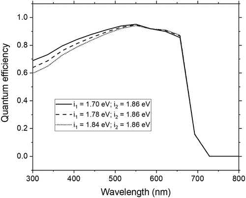
shows the quantum efficiency analyzed and calculated with change in the i1, i2 layer bandgaps, using optimized WFITO of 5.7 eV, in order to obtain the Dint solar cell’s outstanding performance. The photocurrent density, (
) denotes the quantum efficiency as stated in (Yang et al., Citation2016).
Figure 11. Simulated quantum efficiency of the Dint solar cell structure with i1-i2 layer bandgaps for optimized the front contact barrier of 5.7 eV.
Where, ,
,
,
,
, and
are the unit charges, wavelength of light absorbed by Dint solar cell, Planck’s constant, speed of light in vacuum, the solar spectral irradiance under 1.5 G air mass, and the external quantum efficiency, respectively. As previously mentioned, with change in the i1 layer bandgaps (1.70 eV, 1.78 eV, 1.84 eV), and a constant i2 layer bandgap of 1.86 eV, there is a possibility of improving the quantum efficiency in the spectrum wavelength range from 300–550 nm, due to the additional electric field and reduced dangling bond density, consequently, more excitonic generated are separated at p/i interface, leading to higher JSC, (); Hao et al., Citation2019).
shows the simulated optimized Dint solar cell’s J-V characteristic. The VOC,JSC, FF, and Eff are possibly enhanced with the higher work function of 4.9–5.7 eV and (i1)a-Si:H and (i2)a-Si:H layer bandgaps from 1.70 to 1.86 eV. shows the comparison results with other simulation results for the p-i1-i2-n solar cell structure.
Figure 12. Simulated J-V characteristic under light for the Dint solar cell bandgaps for optimized the front contact barrier of 5.7 eV.
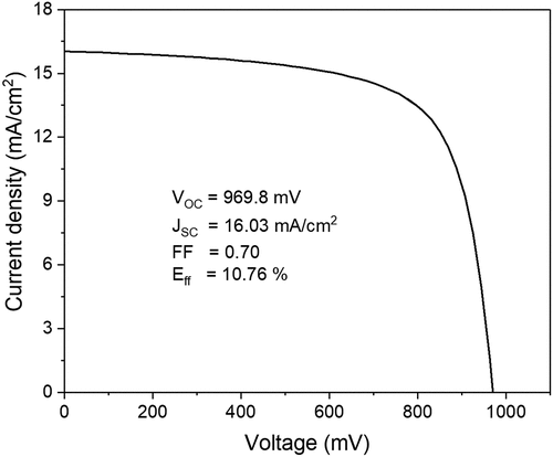
Table 3. Comparison of several simulation results of the p-i1-i2-n solar cell structures
4. Conclusion
In Summary, the ITO/(p)a-Si:H/(i)a-Si:H/(n)a-Si:H/metal (Sint) and ITO/(p)a-Si:H/(i1)a-Si:H/(i2)a-Si:H/(n)a-Si:H/metal (Dint)’s performances were successfully investigated, using AFORS-HET software. The front work function WFITO on performances of the Sint and Dint solar cells was first simulated. Through simulation, the WFITO value was varied from 4.9 to 5.7 eV, in order to determine the optimum WFITO for high solar cell efficiency, confirmed with the J-V dark characteristic, the band diagram in thermodynamics equilibrium, build-in electric field distribution, trapped holes density, and the quantum efficiency. At WFITO = 5.7 eV, the Sint and Dint solar cells had a maximum efficiency of about 6.73 % (VOC = 839.4 mV, JSC = 14.78 mA/cm2, and FF = 54.25 %) and 9.21 % (VOC = 858.1 mV, JSC = 16.07 mA/cm2, and FF = 66.80 %), respectively. Furthermore, in an effort to enhance the Dint solar cell’s electrical and optical properties, the i1-i2 layer bandgaps’ serial structures were optimized to created more excitonic states in the absorber layers, and consequently, improve the cell’s performance. The Dint solar cell was discovered to have a maximum efficiency of 10.76 % (VOC = 969.8 mV, JSC = 16.03 mA/cm2, and FF = 70 %), with WFITO, i1 layer bandgap, and i2 layer bandgap of 5.7 eV, 1.82 eV, and 1.86 eV, respectively. Subsequently, the simulation results were compared with other relevant thin film solar cell simulation results. It can be seen that the structure with adding an intrinsic layer to the p-i-n structure solar cell produces a higher VOC and good conversion efficiency.
Acknowledgements
One of the authors (DH) would like to thankfully acknowledges to the Ministry of Finance Republic of Indonesia for which provided the financial grant needed to carry out this research through BUDI-LPDP scholarship (Grant number: PRJ-5441/LPDP.3/2016). The authors are also grateful to Helmholtz-Zentrum Berlin for the AFORS-HET Software.
Disclosure statement
No potential conflict of interest was reported by the author(s).
Additional information
Funding
Notes on contributors
Dadan Hamdani
Dadan Hamdani received Ph.D. degrees from Department of Physics, Institut Teknologi Sepuluh Nopember, Surabaya, Indonesia. Currently he is Associate Professor in the Department of Physics, FMIPA, Mulawarman University, Samarinda, Indonesia. His current research is focused on modelling of amorphous thin film solar cells and photovoltaic-thermal (PV/T) system.

Darminto Darminto
Darminto Darminto received Ph.D. degrees from the Department of Physics, Bandung Institute of Technology, Bandung, Indonesia. Currently he is with the Department of Physics Institut Teknologi Sepuluh Nopember, Surabaya, Indonesia, as Full Professor. His present research interests include superconductivity, Magneto-electronics, and Nano-and 2D materials.
References
- Abega, F. X. A., Ngoupo, A. T., & Ndjaka, J. M. B. (2021). Numerical design of ultrathin hydrogenated amorphous silicon-based solar cell. International Journal of Photoenergy, 2021, 7506837. https://doi.org/10.1016/j.solmat.2013.11.031
- Ahmad, G., Mandal, S., Barua, A. K., Bhattacharya, T. K., & Roy, J. N. (2017). Band offset reduction at defect-rich p/i interface through a wide bandgap a-SiO:H buffer Layer. IEEE Journal of Photovoltaics, 7(2), 414. https://doi.org/10.1109/JPHOTOV.2016.2642644
- Bechane, L., Bouarissa, N., & Loucif, K. (2021). Numerical simulation and optimization of the performances of a solar cell (p-i-n) containing amorphous silicon using AMPS-1D. Transactions on Electrical and Electronic Materials, 22(4), 531. https://doi.org/10.1007/s42341-020-00262-4
- Belfar, A. (2015). simulation study of the a-si:h/nc-si:h solar cells performance sensitivity to the tco work function, the band gap and the thickness of i-a-si:H absorber layer. Solar Energy, 114, 408–16. https://doi.org/10.1016/j.solener.2015.02.010
- Benigno, I., & Darminto, D. (2017). Effect of intrinsic layer energy gap and thicknesses optimization on the efficiency of P-i-n amorphous silicon solar cell. IJOS, 21, 37–42. http://dx.doi.org/10.12962/j23378530.v2i3.a3184
- Cruz, A., Wang, E.-C., Morales-Vilches, A. B., Meza, D., Neubert, S., Szyszka, B., Schlatmann, R., & Stannowski, B. (2019). Effect of front TCO on the performance of rear-junction silicon heterojunction solar cells: Insights from simulations and experiments. Solar Energy Materials and Solar Cells, 195, 339–345. https://doi.org/10.1016/j.solmat.2019.01.047
- Green, M., Dunlop, E., Hohl-Ebinger, J., Yoshita, M., Kopidakis, N., & Hao, X. (2021). Solar cell efficiency tables (version 57). Progress in Photovoltaics: Research and Applications, 29(1), 3–15. https://doi.org/10.1002/pip.3371
- Hamdani, D., Prayogi, S., Cahyono, Y., Yudoyono, G., & Darminto, D. (2022). The effects of dopant concentration on the performances of the A-SiOx:H(p)/a-Si:H(I1)/a-Si:H(I2)/Μc-Si:H(n) heterojunction solar cell. International Journal of Renewable Energy Development, 11(1), 173. https://doi.org/10.14710/ijred.2022.40193
- Hao, L., Zhang, M., Ni, M., Shen, X., & Feng, X. (2019). Simulation of a silicon heterojunction solar cell with a gradient doping emitter layer. Journal of Electronic Materials, 48(7), 4688. https://doi.org/10.1007/s11664-019-07241-3
- Herasimenka, S. Y., Dauksher, W. J., Boccard, M., & Bowden, S. (2016). ITO/SiOx:H Stacks for silicon heterojunction solar cells. Solar Energy Materials and Solar Cells, 158, 98–101. https://doi.org/10.1016/j.solmat.2016.05.024
- Hernández-Como, N., & Morales-Acevedo, A. (2010). Simulation of hetero-junction silicon solar cells with AMPS-1D. Solar Energy Materials and Solar Cells, 94(1), 62. https://doi.org/10.1016/j.solmat.2009.05.021
- Hussain, S. Q., Kim, S., Ahn, S., Balaji, N., Lee, Y., Lee, J. H., & Yi, J. (2014). Influence of high work function ITO:Zr films for the barrier height modification in a-Si:H/c-Si Heterojunction solar cells. Solar Energy Materials and Solar Cells, 122 , 130–135. https://doi.org/10.1016/j.solmat.2013.11.031
- Jensen, N., Hausner, R. M., Bergmann, R. B., Werner, J. H., & Rau, U. (2002). Optimization and characterization of amorphous/crystalline silicon heterojunction solar cells. Progress in Photovoltaics: Research and Applications, 10(1), 1–13. https://doi.org/10.1002/pip.398
- Khokhar, M. Q., Hussain, S. Q., Pham, D. P., Park, H., Sultana, I., Razaq, A., Chavan, G. T., Kim, Y., Cho, E. C., & Yi, J. (2020). ITO: Zr Bi-layers deposited by reactive O2 and Ar plasma with high work function for silicon heterojunction solar cells. Current Applied Physics, 20(8), 994. https://doi.org/10.1016/j.cap.2020.06.006
- Kim, K.-P., Hussain, A. M., Hwang, D.-K., Woo, S.-H., Lyu, H.-K., Baek, S.-H., Jang, Y., & Kim, J.-H. (2009). Work function modification of indium–tin oxide by surface plasma treatments using different gases. Japanese Journal of Applied Physics, 48(2), 021601. https://doi.org/10.1143/JJAP.48.021601
- Klein, A., Körber, C., Wachau, A., Säuberlich, F., Gassenbauer, Y., Harvey, S. P., Proffit, D. E., & Mason, T. O. (2010). Transparent conducting oxides for photovoltaics: Manipulation of fermi level, Work Function and Energy Band Alignment, Materials, 3(11), 4892–4914. https://doi.org/10.3390/ma3114892
- Kumar, A., & Ranjan, P. (2020). Impact of light soaking on absorber and buffer layer in thin film solar cells. Applied Physics A, 126(6), 397. https://doi.org/10.1007/s00339-020-03595-2
- Oh, W.-K., Hussain, S. Q., Lee, Y.-J., Lee, Y., Ahn, S., & Yi, J. (2012). Study on the ITO work function and hole injection barrier at the interface of ITO/a-Si:H(p) in amorphous/crystalline silicon heterojunction solar cells. Materials Research Bulletin, 47(10), 3032. https://doi.org/10.1016/j.materresbull.2012.04.106
- Park, J., Dao, V. A., Shin, C., Park, H., Kim, M., Jung, J., Kim, D., & Yi, J. (2013). A buffer-layer/a-SiOx:H(p) window-layer optimization for thin film amorphous silicon based solar cells. Thin Solid Films, 546, 331–336. https://doi.org/10.1016/j.tsf.2013.06.064
- Park, Y. S., Kim, E., Hong, B., & Lee, J. (2013). Characteristics of ITO films with oxygen plasma treatment for thin film solar cell applications. Materials Research Bulletin, 48(12), 5115. https://doi.org/10.1016/j.materresbull.2013.07.026
- Park, K. M., Shin, J. W., Son, W. H., Lee, T. Y., & Choi, S. Y. (2012). Study of the P-i-n layer to enhance a-Si:H solar cell efficiency based on single junction. Molecular Crystals and Liquid Crystals, 565, 106–114. https://doi.org/10.1080/15421406.2012.693287
- Prayogi, S., Cahyono, Y., Iqballudin, I., Stchakovsky, M., & Darminto, D. (2021). The effect of adding an active layer to the structure of A-Si: H solar cells on the efficiency using RF-PECVD. Journal of Materials Science: Materials in Electronics, 32(6), 7609–7618. https://doi.org/10.1007/s10854-021-05477-6
- Rached, D., & Mostefaoui, R. (2008). Influence of the front contact barrier height on the indium tin oxide/hydrogenated p-doped amorphous silicon heterojunction solar cells. Thin Solid Films, 516(15), 5087. https://doi.org/10.1016/j.tsf.2008.02.031
- Shin, C., Iftiquar, S. M., Park, J., Kim, Y., Kim, S., Jung, J., & Yi, J. (2017). Development of highly conducting N-type micro-crystalline silicon oxide thin film and its application in high efficiency amorphous silicon solar cell. Materials Science in Semiconductor Processing, 66, 223–231. https://doi.org/10.1016/j.mssp.2017.05.002
- Singh, S., Kumar, S., & Dwivedi, N. (2012). Band gap optimization of p–i–n Layers of a-Si:H by computer aided simulation for development of efficient solar cell. Solar Energy, 86(5), 1470. https://doi.org/10.1016/j.solener.2012.02.007
- Son, W. H., Lee, T. Y., Choi, S. Y., & Jung, D. (2018). effect of phosphorus doping on the performance of pin-type a-Si:H thin-film solar cells. Molecular Crystals and Liquid Crystals, 662(1), 25–31. https://doi.org/10.1080/15421406.2018.1466237
- Stangl, R. (2010). Numerical simulation of solar cells and solar cell characterization methods: the open-source on demand program AFORS-HET. In C. Leendertz (Ed.), Solar energy (pp. 14). IntechOpen.
- Sturiale, A., Li, H. T., Rath, J. K., Schropp, R. E. I., & Rubinelli, F. A. (2009). Exploring Dark Current Voltage Characteristics of Micromorph Silicon Tandem Cells with Computer Simulations. Journal of Applied Physics, 106(1), 14502. https://doi.org/10.1063/1.3151691
- Sultana, R. S., Bahar, A. N., Asaduzzaman, M., & Ahmed, K. (2017). Numerical modeling of a CdS/CdTe photovoltaic cell based on ZnTe BSF Layer with optimum thickness of absorber layer. Cogent Engineering, 4(1). https://doi.org/10.1080/23311916.2017.1318459
- Yang, Z., Shang, A., Qin, L., Zhan, Y., Zhang, C., Gao, P., Ye, J., & Li, X. (2016). Broadband and wide-angle light harvesting by ultra-thin silicon solar cells with partially embedded dielectric spheres. Optics Letters, 41(7), 1329. https://doi.org/10.1364/OL.41.001329
- Zhang, B. (2010). Influence of oxygen flow rate on microstructural, electrical and optical properties of indium tin tantalum oxide films. Materials Science in Semiconductor Processing, 13(5–6), 411. https://doi.org/10.1016/j.mssp.2011.10.004