
Abstract
The layered Bi-chalcogenide compounds have been drawing much attention as a new layered superconductor family since 2012. Due to the rich variation of crystal structure and constituent elements, the development of new physics and chemistry of the layered Bi-chalcogenide family and its applications as functional materials have been expected. Recently, it was revealed that the layered Bi chalcogenides can show a relatively high thermoelectric performance (ZT = 0.36 in LaOBiSSe at ~650 K). Here, we show the crystal structure variation of the Bi-chalcogenide family and their thermoelectric properties. Finally, the possible strategies for enhancing the thermoelectric performance are discussed on the basis of the experimental and the theoretical facts reviewed here.
Public Interest Statement
This article reviews the crystal structure variation of new Bi-chalcogenide layered compound family and their thermoelectric properties. Since 2012, the Bi-chalcogenide compounds have been drawing attentions as a new class of layered superconductor. Recently, we revealed that the parent phases of those Bi-chalcogenide superconductors are possible candidate of new thermoelectric materials. So far, the highest thermoelectric performance (ZT: dimensionless figure of merit) have reached ZT = 0.36 in LaOBiSSe. Here, we discuss the evolution of thermoelectric properties when the structure of layers (electrically conducting layers and/or insulating layers). Finally, the possible strategies for the enhancement of thermoelectric properties in the Bi-chalcogenide compounds are proposed.
1. Introduction
Thermoelectric energy conversion is a promising technology for solving energy problems because the energy of the waste heat can be directly converted to the electrical energy. So far, the available thermoelectric devises have been limited due to the absence of high-performance thermoelectric materials. To estimate the performance of thermoelectric materials, dimensionless figure-of-merit (ZT) is generally used. The ZT can be calculated as ZT = S2T/ρκ, where S, T, ρ, and κ are the Seebeck coefficient, absolute temperature, electrical resistivity, and thermal conductivity, respectively. Hence, a large absolute value of the Seebeck coefficient, low electrical resistivity, and low thermal conductivity are required for a high ZT. Typically, in a conventional semiconductor, S is proportional to T/n, where n is the carrier concentration with a single-band approximation. The ρ is proportional to 1/enμ, where μ is the carrier mobility. Therefore, insulators (or semiconductors with a large band gap) exhibit large absolute S, but their ρ is usually large. In contrast, metallic compounds exhibit low ρ, but absolute S of metallic compounds is generally small. Due to this trade-off relationship of the electrical factors (S and ρ), the enhancement of S2/ρ (power factor: PF) is quite difficult. The material, which satisfies both large S and low ρ, is semiconductors with a narrow band gap (Shakouri, Citation2011). For example, the Bi2Te3 family possesses such a band structure and shows a high performance of ZT ~1 at around 300 K due to the large μ and the suitable n (Chung et al., Citation2000; Nolas, Sharp, & Goldsmid, Citation2001). Hence, Bi2Te3-based compounds have been used as a practical thermoelectric material for a long time (Nolas et al., Citation2001). Another strategy for enhancing ZT is the use of the quantum-size effect. The ZT of Bi2Te3-based system can be enhanced up to 2.4 by fabricating the Bi2Te3/Sb2Te3 superlattice device (Hicks & Dresselhaus, Citation1993; Venkatasubramanian, Siivola, Colpitts, & O’Quinn, Citation2001). In addition, the quantum-size effect can be expected to positively work in enhancing ZT in the compounds with a layered structure. One of the examples is the layered Co oxides, such as NaCoO2 and related layered compounds (Funahashi et al., Citation2000; Shikano & Funahashi, Citation2003; Takahata, Iguchi, Tanaka, Itoh, & Terasaki, Citation2000). These compounds show anomalously large S owing to the strong electron correlations, and the κ of these compounds is reduced by the phonon scattering at the interface of the layers. In addition, layered compounds typically possess the great flexibilities of stacking structure and constituent elements as demonstrated in the Co oxides (Funahashi et al., Citation2000; Shikano & Funahashi, Citation2003; Takahata et al., Citation2000), which results in the desirable tuning of the electronic structure and the local crystal structure. Therefore, one can say that the layered structure is greatly suitable for designing high ZT materials.
In 2012, we discovered new layered superconductors whose crystal structure is composed of the alternate stacks of the BiS2 bilayer (electrically conducting layer) and the electrically insulating blocking layers (Mizuguchi, Citation2015; Mizuguchi, Fujihisa, et al., Citation2012; Mizuguchi, Demura, et al., Citation2012). The parent phase (for example, LaOBiS2 with the structure of Figure (a)) is a semiconductor with a band gap (Mizuguchi, Fujihisa, et al., Citation2012; Usui, Suzuki, & Kuroki, Citation2012). When electron carriers were generated in the Bi-6p orbitals by partial substitutions of O by F (in the La2O2 blocking layers), the F-substituted compounds (LaO1−xFxBiS2) becomes metallic and shows superconductivity at low temperatures (Mizuguchi, Demura, et al., Citation2012; Usui et al., Citation2012). Furthermore, the La2O2 blocking layer can be replaced by the RE2O2 layers (RE: rare earth or Bi) or other oxide (or fluoride) layers as shown in Figure . Indeed, the crystal structure can be flexibly modified by changing the blocking layer structure in the BiS2-based compound family (Mizuguchi, Citation2015). Focusing on the electronic state, we noted that the calculated bad gap was relatively small, and some parent compounds showed low electrical resistivity (as compared normal semiconductors). In addition, the thermal conductivity of the LaO1−xFxBiS2 samples was relatively small (Pallecchi et al., Citation2014). Thus, we considered that the BiS2-based layered compounds could be a layered thermoelectric material family as the Bi–Te family or the layered Co oxides family. In this article, the crystal structure variation of the layered Bi-chalcogenide family and the physical properties of those Bi chalcogenides are reviewed. Finally, the possible strategies for enhancing thermoelectric properties of the Bi chalcogenides are discussed.
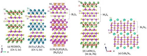
Figure 1. Schematic images of the crystal structure of various Bi-chalcogenide compounds. ((a)–(c)) Typical BiS2-based compounds: (a) REOBiCh2 (RE: rare earth or Bi; Ch: S, Se) (Maziopa et al., Citation2014; Mizuguchi, Demura, et al., Citation2012), (b) Eu3F4Bi2Ch4 (Zhai, Zhang, et al., Citation2014; Zhang et al., Citation2015), and (c) Bi4O4SO4Bi2S4 (Mizuguchi, Fujihisa, et al., Citation2012). The electrically conducting layer of these compounds is the two-layer-type Bi2S4 layer. (d) LaOM2S3 (M: Bi, Pb) (Sun et al., Citation2014). The M4S6 conducting layer of LaOM2S3 is similar to the Bi4Te6 layer of (e) CsBi4Te6 (Chung et al., Citation2000).
This article contains new (unpublished) results on CeO1−xFxBiS2, NdO1−xFxBiS2, and LaOBiPbS3. Therefore, we briefly explain the experimental procedures. The polycrystalline samples were prepared using a conventional solid-state reaction method with reaction temperatures of 700–800°C. The purity and the crystal structure of the obtained samples were investigated using powder X-ray diffraction. The reaction or the annealing processes were carried out in an evacuated quartz tube. Temperature dependence of ρ and S were measured using a four-terminal method with ZEM-3 (Advance Riko).
2. Crystal structure of layered Bi chalcogenides
Typical crystal structures of the layered Bi chalcogenides are summarized in Figure . All the compounds have a layered structure composed of the alternate stacks of the electrically conducting layer and the electrically insulating blocking layer. The typical structures are categorized into the tetragonal (P4/nmm or I4/mmm) space group. These Bi chalcogenides have NaCl-type Bi-Ch conducting layers: Bi2Ch4 layer (BiCh2 bilayer) or M4Ch6 layer (M: Bi, Pb). Since the conducting layers contain a two-dimensional Bi-Ch square lattice, the layered Bi chalcogenides exhibit two-dimensional electrical transport.
Figure ((a)–(c)) is the crystal structure of BiS2-based compounds with the BiS2 bilayer (Bi2S4 layer) as a conducting layer. Among them, the REOBiCh2 (RE: rare earth or Bi; Ch: S or Se) structure (Figure (a)) is the most popular one. In this structure, the Bi2S4 layer is a conducting layer, and the RE2O2 layer acts as a blocking layer. When electron carriers were doped by partial substitutions of O by F, the RE(O,F)BiCh2 compounds become a superconductor with a superconducting transition temperature (Tc) as high as 11 K (Mizuguchi, Citation2015; Mizuguchi, Demura, et al., Citation2012). The RE site of RE(O,F)BiS2 can be occupied by La, Ce, Pr, Nd, Sm, Yb, and Bi (Demura et al., Citation2013; Jha, Kumar, Kumar Singh, & Awana, Citation2013; Miura et al., Citation2016; Mizuguchi, Demura, et al., Citation2012; Nagao, Citationin press; Okada, Ogino, Shimoyama, & Kishio, Citation2015; Shao et al., Citation2015; Thakur et al., Citation2015; Xing, Li, Ding, Yang, & Wen, Citation2012; Yazici et al., Citation2012). In the case of RE = La, the RE site can be partially substituted with Y, Ti, Zr, Hf, and Th (Jeon, Yazici, White, Friedman, & Maple, Citation2014; Yazici et al., Citation2013). In addition, the S site can be substituted by Se. The RE(O,F)BiS2−xSex-type compounds were reported for RE = La, Ce, and Nd (Hiroi, Kajitani, Omachi, Miura, & Mizuguchi, Citation2015a, 2015b; Mizuguchi, Hiroi, & Miura, Citationin press; Tanaka et al., Citation2015; Wang et al., Citationxxxx). Furthermore, the end member La(O,F)BiSe2 can be synthesized for RE = La (Maziopa et al., Citation2014).
The RE2O2 layer of the REOBiS2 structure can be replaced with the Sr2F2 or Eu2F2 layer, which results in the SrFBiS2 or EuFBiS2 compound (Lei, Wang, Abeykoon, Bozin, & Petrovic, Citation2013; Lin et al., Citation2013; Zhai, Tang, et al., Citation2014). The Sr (or Eu) site can be partially substituted by RE; the RE substitution dopes electron carriers into the BiS2 layer (Jha, Tiwari, & Awana, Citation2015; Zhai et al., Citation2015). In addition, the Sr site can be partially substituted by Ca (Zhai, Tang, et al., Citation2014). Owing to these great flexibility on element substitutions for the RE and Ch sites, the REOBiCh2-type structure has been actively studied, and is particularly important to understand the physical properties of the layered Bi–chalcogenide family.
Figure (b) is a crystal structure of Eu3F4Bi2S4 (Zhai, Tang, et al., Citation2014) with a Eu3F4 blocking layer. The Eu3F4 layer can be regarded as the double Eu2F2 layers combined to each other with Eu-site sharing. The material itself is a superconductor, and the superconducting Tc was enhanced by Se substitution in Eu3F4Bi2S2−xSex (Zhang et al., Citation2015).
Figure (c) is a crystal structure of Bi4O4SO4Bi2S4, whose structure can be regarded as the alternate stacks of the Bi4O4SO4 blocking layer and the Bi2S4 conducting layer (BiS2 bilayer). It has been considered that the SO4 site in the blocking layer can have some defects, which provides electron carriers into the BiS2 layers (Mizuguchi, Fujihisa, et al., Citation2012). Indeed, the Bi4O4S3 compound with 50% SO4 defects (namely, Bi4O4(SO4)0.5Bi2S4) becomes a superconductor with Tc ~ 5 K (Mizuguchi, Fujihisa, et al., Citation2012). Due to the difficulty in determining the SO4 site structure using polycrystalline samples and the absence of single crystals, the precise determination of the SO4 site structure (and the composition) has not been achieved yet (Miura et al., Citation2015); some reports suggested the Bi3O2S3 (= Bi4O4S2Bi2S4) phase was also formed and showed superconductivity (Li et al., Citation2015; Phelan et al., Citation2013).
Recently, a new Bi-chalcogenide compound with a thick conducting layer of M4S6 (M = Bi, Pb) was synthesized. Figure (d) shows the crystal structure of LaOBiPbS3 (Sun et al., Citation2014). In this structure, an NaCl-type M–S block (layer) is intercalated at between BiS2 layers. Also, this conducting layer can be regarded as the four-layer-type structure. Thus, the crystal structure variation can be developed by fabricating the multi-layer-type conducting layers as well as by changing the blocking layer structure as demonstrated in the structures of Figure ((a)–(c)). We note that the distorted NaCl-type M4S6 conducting layer is structurally similar to the Bi4Te6 conducting layer of CsBi4Te6, which is a known thermoelectric material (Figure (e)) (Chung et al., Citation2000), although the space group of CsBi4Te6 (monoclinic C2/m) is different from that of LaOBiPbS3 and the BiS2-based compounds (tetragonal P4/nmm or I4/mmm). The structural symmetry lowering from tetragonal to monoclinic was recently revealed in a single crystal of LaOBiS2 by synchrotron X-ray experiments (Sagayama et al., Citation2015). Although the X-ray diffraction (XRD) with the polycrystalline LaOBiS2 samples suggested the space group of tetragonal P4/nmm, the crystal structure of the LaOBiS2 single crystal was determined to be monoclinic P21/m. This different results in between polycrystalline and single-crystal samples would indicate the crystal structure instability in the BiS2-based compounds. At the same time, the structure instability can be regarded as the structure flexibility in the same group of compounds. Thus, we consider that the Bi-chalcogenide family possesses great flexibility of crystal structure (including space group, stacking sequence, and constituent elements), and hence, it is very useful to explore new materials with a high thermoelectric performance.
3. Thermoelectric properties of LaOBiS2-based compounds
3.1. LaO1−xFxBiS2
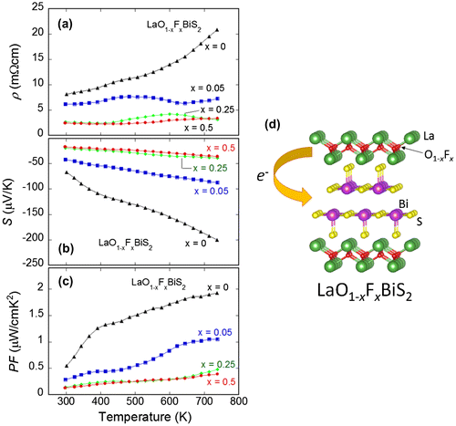
Here, we focus on the LaOBiS2 systems. As introduced above, LaOBiS2 is one of the parent phases of the BiS2-based superconductor, and shows semiconducting-like electrical transport below the room temperature (Mizuguchi, Demura, et al., Citation2012). Band calculations suggested that the LaOBiS2 is a semiconductor with a relatively narrow band gap (< 1 eV) (Usui et al., Citation2012). Partial substitutions of the O site by F generate electron carriers in the BiS2 conducting layers, and the F-substituted LaO1−xFxBiS2 shows a superconducting transition at low temperatures (Mizuguchi, Demura, et al., Citation2012). We considered the LaOBiS2-based compounds could exhibit a high thermoelectric property since we observed a low thermal conductivity in the LaO1−xFxBiS2 samples (κ ~ 2 W/mK at 300 K) (Pallecchi et al., Citation2014). Thus, we measured high-temperature thermoelectric properties (ρ, S, and PF) of LaO1−xFxBiS2 and investigated the effect of the F substitution (electron doping) to the thermoelectric properties (Omachi, Kajitani, Hiroi, Miura, & Mizuguchi, Citation2014).
Figure ((a)–(c)) shows the temperature dependences of (a) ρ, (b) S, and (c) PF for LaO1−xFxBiS2. As depicted in Figure (d), the electron carrier concentration is expected to increase with increasing F concentration. The ρ of x = 0 increases with increasing temperature, and an anomaly (a hump) is observed at around 500 K. Although the origin of the anomaly has not been clarified yet, it may be related to the (local) structure distortion because the crystal structure of LaOBiS2 can be distorted into monoclinic as revealed in the single-crystal structure analysis using synchrotron X-ray (Sagayama et al., Citation2015). With increasing F concentration, the values of ρ decrease at whole temperatures. The S was negative for all the F concentration at whole temperatures (tested in these experiments), which indicates that the mainly contributing carrier is electron in this system. The absolute value of S increases with increasing temperature. One of the important facts is the absolute S largely decreases with increasing F concentration. As a result, the values of the PF rapidly decrease with F substitution as shown in Figure (c). Indeed, in the LaOBiS2 system, the electron doping obviously degrades the thermoelectric properties (Omachi, Kajitani, et al., Citation2014; Pallecchi et al., Citation2014). To enhance the thermoelectric performance (PF) in the LaOBiS2 system, decreasing ρ without degradation of the absolute S is required. Thus, we next investigated the effects of partial substitutions of S by Se in the conducting layers.
Figure 2. ((a)–(c)) Temperature dependences of (a) electrical resistivity (ρ), (b) Seebeck coefficient (S), and (c) power factor (PF) for LaO1−xFxBiS2. (d) Schematic image of the crystal structure of LaO1−xFxBiS2 and electron doping scenario.
3.2. LaOBiS2−xSex
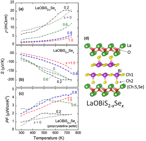
The S site of LaOBiS2 can be partially substituted by Se (Mizuguchi et al., Citation2014). In LaOBiS2−xSex, both S and Se have the same valence of −2 (S2− and Se2−). Hence, the Se substitution does not affect the valence of Bi and does not dope electrons, but it should affect the band structure because of the difference of ionic radii of S2− (184 pm) and Se2− (198 pm). Upon the substitution of larger Se2−, the enhancement of the orbital overlap between Bi and Ch should be expected.
Figure ((a)–(c)) shows the temperature dependences of (a) ρ, (b) S, and (c) PF for LaOBiS2−xSex (Mizuguchi et al., Citation2014). Figure (d) is the crystal structure of LaOBiS2−xSex and the definitions of the Ch1 and the Ch2 sites. With increasing Se concentration, the values of ρ decrease, indicating that the Se substitution enhances electric conductivity in LaOBiS2−xSex. The values of S are all negative as observed in LaO1−xFxBiS2, which suggests that the electrons are mainly contributing in electrical transport in LaOBiS2−xSex. The absolute values of S do not show a remarkable change up to x = 0.6, and it slightly decreases at x = 0.8 and 1. The small changes in the S with increasing Se concentration imply that the carrier concentration is not largely affected by the Se substitution. In addition, as will be shown later, the densified LaOBiSSe sample shows the S value comparable to that of LaOBiS2. Thus, we consider that the Se substitution does not largely affect carrier concentration, but it enhances metallic conductivity due to the enhanced carrier mobility; actually, the large enhancement of mobility with increasing Se concentration was revealed in our recent Hall measurements (Nishida, Nishiate, Lee, Miura, & Mizuguchi, Citation2015). This can be understood with the concept of in-plane chemical pressure effect as demonstrated in REO0.5F0.5BiCh2-type superconductors (Mizuguchi et al., Citation2015). The increase in Se concentration in the Bi–Ch plane results in the enhancement of orbital overlaps between Bi and Ch. It can be considered that the enhanced orbital overlap enhances the carrier mobility, and hence, the metallic conductivity is enhanced. Finally, the calculated PF is shown in Figure (c) as a function of temperature. The PF is clearly enhanced with increasing Se concentration, and large PF values exceeding 4 μW/cmK2 are observed for x = 0.8 and 1 in LaOBiS2−xSex. Indeed, the Se substitution largely enhances the thermoelectric performance in the LaOBiS2 system.
Figure 3. ((a)–(c)) Temperature dependences of (a) electrical resistivity (ρ), (b) Seebeck coefficient (S), and (c) power factor (PF) for LaOBiS2−xSex. (d) Schematic image of the crystal structure of LaOBiS2−xSex and the definitions of the Ch1 and Ch2 sites.
3.3. Densified LaOBiSSe
The experimental results on LaOBiS2−xSex shown above were based on the polycrystalline pellet samples with a typical relative density of 85–90%. Thus, we densified the LaOBiS2−xSex samples using a hot-press (HP) instrument under an applied pressure of 50 MPa and annealing temperature of 700 or 800°C, with which high-density samples were obtained (relative density >97%) (Nishida, Miura, Lee, & Mizuguchi, Citation2015; Nishida, Nishiate et al., Citation2015). Here, we show the thermoelectric properties of LaOBiSSe because the highest performance was attained in the HP-LaOBiSSe sample among x = 0–1.
Due to the uniaxial pressure in the densification process, the obtained sample can possess anisotropic crystal (grain) orientation. So, let us firstly mention the crystal orientation of the HP sample. Figure (a) shows the XRD patterns for the powder and pellet samples; for the pellet samples, the scattering vector of X-ray is parallel or perpendicular to the pressing (HP) direction (P// or P⊥). The definitions of the P// and P⊥ directions are shown in Figure (b). The XRD results propose that the HP process does not affect the phase purity because any impurity phases were not generated. The peak intensities were different in between P// and P⊥, indicating that the obtained sample was oriented as expected. However, we found that the crystal orientation in the HP sample was very weak: the difference of the peak intensities of the (h00) and the (00 l) peaks for P// and P⊥ are not large. (If the sample was completely oriented, only the (h00) or the (00 l) peaks should be observed as in the case of thin films.)
Figure 4. (a) XRD patterns for hot-pressed (HP) LaOBiSSe (x = 1). The Miller indices are shown with the top profile. The asterisk indicates the impurity (La2O3: 7% against the major phase) peak. To investigate the crystal structure anisotropy, XRD measurements were performed for polished pellets with two scattering vectors of P// and P⊥. (b) Schematic image for the definitions of the measurement directions of P// and P⊥ and the hot-pressing direction. ((c)–(f)) Temperature dependences of (c) electrical resistivity (ρ), (d) Seebeck coefficient (S), (e) thermal conductivity (κ), and dimensionless figure-of-merit (ZT) for HP-LaOBiSSe.
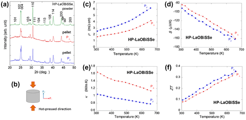
Figure (c) shows the temperature dependences of ρ for two measurement directions (measured with currents of I // P// or I // P⊥). The ρ increases with increasing temperature for both, and the values of ρ for P⊥ are clearly lower than those of P//, which is consistent to the fact that the ab plane of the LaOBiSSe grains is relatively oriented along the P⊥ direction. The BiS2-based compounds essentially show two-dimensional electrical conduction (Nagao, Miura, Watauchi, Takano, & Tanaka, Citation2015). Figure (d) shows the temperature dependences of S. For both samples, negative S is observed. The absolute values of S for P// are slightly larger than those of P⊥, which is also consistent with the difference in the ρ and the crystal orientation. As a result, the PF values for P⊥ are larger than those for P//.
To estimate ZT, κ was also measured for these samples (Figure (e)). The κ decreases with increasing temperature, and the values of κ for the P⊥ direction are clearly larger than those for the P// direction. This result indicates that the thermal conductivity along the c-axis is obviously smaller than that along the a-axis. Figure (f) shows the temperature dependences of ZT for both measurement directions. The values of ZT for P// are slightly larger than those for P⊥, and the ZT for these directions at the highest temperature (tested in the study) is almost the same. These results suggest that the thermoelectric performance of LaOBiSSe is not largely affected by the crystal orientation because one direction possesses a good (high) PF, and the other direction possesses a good (low) κ. This characteristic on the insensitivity of ZT to the crystal (grain) orientation may be useful when considering practical application of these BiCh2-based materials.
4. Properties of other layered Bi chalcogenides
Up to here, we focused on the properties of LaOBiS2-based systems. As mentioned with Figure , one of the merits of the Bi-chalcogenide layered compound family is the crystal structure variety. Thus, in this section, we briefly introduce the thermoelectric properties of REO1−xFxBiS2 (RE = Ce or Nd) and EuFBiS2 with the REOBiCh2-type structure. In addition, the properties of LaOBiPbS3 with the four-layer-type compound (Figure (d)) at high temperatures are shown.
4.1. REO1−xFxBiS2
Figure ((a)–(c)) shows the temperature dependences of ρ, S, and PF for CeO1−xFxBiS2 with x = 0, 0.25, and 0.5. The values of ρ for x = 0 (CeOBiS2) are clearly lower than those of LaOBiS2. It has been reported that the polycrystalline sample of CeOBiS2 shows metallic conductivity at low temperature (Xing et al., Citation2012), which seems to be consistent to the present data. In contrast, the single crystal of CeOBiS2 shows semiconducting behavior at low temperatures (Higashinaka et al., Citation2015). On the basis of these diverse experimental facts in polycrystalline samples and single crystals, the electronic states can be different in between these two sample forms. As a fact, the photoemission experiment suggested that the Ce valence is in the mix-valence state of Ce3+ and Ce4+ (Sugimoto et al., Citation2014), which should provide excess electron carriers to the BiS2 conducting layers. Local structure distortion and/or the effect of the grain size may be affecting the Ce valence and the electronic states of polycrystalline CeOBiS2. The low absolute values of S for CeOBiS2 (Figure (b)) seem to be consistent with the mixed-valence scenario in CeOBiS2 because the absolute value of S of semiconductors generally decreases with increasing carrier concentration. As a result, the PF for CeOBiS2 is lower than that of LaOBiS2 and comparable to electron-doped LaO0.95F0.05BiS2.
Figure 5. ((a)–(c)) Temperature dependences of (a) electrical resistivity (ρ), Seebeck coefficient (S), and power factor (PF) for CeO1−xFxBiS2. ((d)–(f)) Temperature dependences of (d) ρ, (e) S, and (f) PF for NdO1−xFxBiS2.
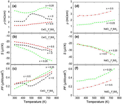
For x = 0.25 of CeO1−xFxBiS2, the values of ρ are larger than those for x = 0. The absolute values of S for x = 0.25 are also larger than those of x = 0. For x = 0.5, the values of ρ and absolute S are lower than those for x = 0. These experimental results suggest that the effects of F substitutions to the thermoelectric properties in CeO1−xFxBiS2 cannot be simply understood. First, we have to consider the effect of the mixed-valence states of Ce. In addition, we are tuning electron carriers by the F concentration. Furthermore, the carrier mobility should largely affect the electrical transport as shown in LaOBiS2−xSex. Actually, the a-axis is expanded with increasing F concentration in these CeO1−xFxBiS2 samples and in the previous reports as well (Xing et al., Citation2012). By simply estimating the in-plane chemical pressure effect in CeO1−xFxBiS2, the elongation of the a-axis should result in the decrease in in-plane chemical pressure (decrease in orbital overlap) and carrier mobility. These multiple factors make the understanding of the thermoelectric properties of CeO1−xFxBiS2 quite difficult. Anyway, the replacement of the La2O2 blocking layer to the Ce2O2 layer does not positively work in enhancing PF.
Next, let us introduce the properties of NdO1−xFxBiS2 with x = 0.25 and 0.5; unfortunately, the polycrystalline samples of x = 0 cannot be obtained in the system. Figure ((d)–(f)) shows the temperature dependences of ρ, S, and PF for NdO1−xFxBiS2. Both samples show similar temperature dependences of ρ and S, but the values of ρ for x = 0.25 are lower than those for x = 0.5, while the nominal composition of doped F is half in the x = 0.25 sample. The almost same values of S would suggest that the effective carrier concentration is almost the same. This assumption is consistent with the fact that the superconducting transition temperature of the NdO1−xFxBiS2 system is not sensitive to the F concentration within a wide range of x = 0.1–0.7 (Demura et al., Citation2013; Jha & Awana, Citation2014; Omachi, Hiroi, Kajitani, Miura, & Mizuguchi, Citation2014). The a-axis of NdO1−xFxBiS2 also increases with increasing F concentration. The larger ρ values for x = 0.5 than those for x = 0.25 may be resulting from the decrease in the in-plane chemical pressure with the a-axis elongation as well as in CeO1−xFxBiS2. As facts, the values of PF for NdO1−xFxBiS2 are quite low as compared to LaOBiS2−xSex.
As shown here, the replacement of the La2O2 blocking layer to the other RE2O2 blocking layer does not positively work in enhancing PF. In addition, the Se substitution for the S site cannot be demonstrated in the Ce- or Nd-based compounds. The reason may be due to the ionic radius of Se2−, which would be too large for the Ce2O2 or Nd2O2 blocking layers. Next, we review the recent studies on EuFBiS2 and LaOBiPbS3.
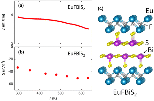
4.2. EuFBiS2
EuFBiS2 crystalizes in the tetragonal P4/nmm space group, which can be obtained by replacing the La2O2 layer of LaOBiS2 to the Eu2F2 layer (Figure (c)). This material shows metallic conductivity and shows a superconducting transition at 0.4 K (Zhai, Tang, et al., Citation2014). Goto et al. measured thermoelectric properties of EuFBiS2 at high temperatures (Goto, Kajitani, Mizuguchi, Kamihara, & Matoba, Citation2015). Figure ((a), (b)) shows the temperature dependences of ρ and S for EuFBiS2. At T = 300–623 K, the ρ showed a slight decrease with increasing temperature but the values were almost constant (ρ = 3.5–4 mΩcm). The S at 300 K was −32 μV/K, and the absolute value of S increased with increasing temperature and reached −50 μV/K at 623 K. The estimated κ at 300 K was about 2 W/mK, which was also low and close to that of LaOBiS2. Indeed, low thermal conductivity seems to be a general characteristic of the layered Bi-chalcogenide family. The calculated PF and ZT were 0.71 μW/cmK2 and 0.02 at 623 K, respectively. We consider that the low ZT (PF) in EuFBiS2 can be attributed to the excess electron carriers as in the case of CeOBiS2. Zhai et al. proposed that the Eu valence in EuFBiS2 is not +2 but +2.1–2.3, and the metallic characteristics were resulting from the excess electron carriers doped in the BiS2 layers due to the mixed-valence state of Eu (Zhai, Tang, et al., Citation2014). The carrier concentration (n) estimated from the Hall measurement is 3.2 × 1021 cm−3, which is clearly larger than those of the parent phases of REOBiS2. Therefore, a high ZT cannot be obtained in EuFBiS2 without compensation of the excess electron carriers in the BiS2 layers.
Figure 6. Temperature dependences of (a) electrical resistivity (ρ) and (b) Seebeck coefficient (S) for EuFBiS2. (c) Schematic image of the crystal structure of EuFBiS2.
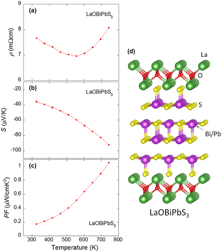
4.3. LaOBiPbS3
As introduced in Figure , LaOBiPbS3 has the four-layer-type conducting layer, which is similar to the Bi4Te6 conducting layer of CsBi4Te6 (Chung et al., Citation2000; Sun et al., Citation2014). Hence, this material is very important to discuss how we can enhance the thermoelectric properties of the Bi-chalcogenide layered compound family. Sun et al. reported thermoelectric properties of LaOBiPbS3 below the room temperature (Sun et al., Citation2014). The ρ at 300 K was ~8 mΩcm, and the ρ largely increased with decreasing temperature (particularly below 100 K). The S at 300 K was −50 μV/K. The κ at 300 K was ~4 W/mK. Using these data, the PF and ZT at 300 K can be calculated to be 0.31 μW/cmK2 and 0.0023, respectively.
We examined the thermoelectric properties of LaOBiPbS3 at high temperatures. Figure ((a)–(c)) shows the temperature dependences of ρ, S and PF for LaOBiPbS3. The values of ρ are 7–8 mΩcm at between 300 and 740 K, and the ρ does not show a large change with increasing temperature. In contrast, the absolute values of S show a large increase with increasing temperature. The S at 740 K is −92 μV/K. Hence, the calculated PF largely increases with increasing temperature and reaches 1 μW/cmK2 at 740 K. Although the values of PF for LaOBiPbS3 are still lower than those for LaOBiSSe, the PF will be enhanced by increasing carrier mobility as demonstrated in LaOBiS2−xSex.
Figure 7. ((a)–(c)) Temperature dependences of (a) electrical resistivity (ρ), Seebeck coefficient (S), and power factor (PF) for LaOBiPbS3. (d) Schematic image of the crystal structure of LaOBiPbS3.
5. Summary and possible strategies for a high thermoelectric performance
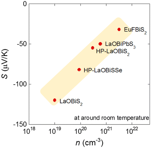
We reviewed the crystal structure variation and the physical properties of the new Bi-chalcogenide layered compound family. Here, we briefly summarize the evolution of thermoelectric properties by the element substitution or the manipulation of the layered structure and would like to discuss the possible strategies for a high thermoelectric performance in the layered Bi-chalcogenide compound family. One of the advantages of the layered Bi-chalcogenide compounds as a thermoelectric material is the low thermal conductivity. The values of κ are quite lower than that of the other chalcogenides or other inorganic materials with electrical conduction. In addition, as shown in the part of LaOBiSSe, the κ decreases with introducing disorder as the Se substitution for the S site in LaOBiS2−xSex. Therefore, the thermal conductivity will be tunable at the final stage of the material design of Bi-chalcogenide thermoelectric materials. Thus, we need to enhance PF at the early stage, and now, we are exploring new materials with PF higher than that of LaOBiSSe. On the basis of the results of the electron doping in LaO1−xFxBiS2, the excess electron carriers should degrade the PF. In addition, the compounds containing self-doped carriers, such as CeOBiS2 or EuFBiS2, show a lower performance due to the excess carriers as well. Namely, the parent compound with a band gap should be preferable for a high PF material, which seems to be consistent with the Mott relationship (S can be expressed as a function of T/n) as used in the study of LaO1−xFxBiS2 (Pallecchi et al., Citation2014). Therefore, the lower n would result in a high absolute value of S in this system. To discuss this assumption, we plotted the n and the S reported in Pallecchi et al. (Citation2014), Zhai, Tang, et al. (Citation2014), Sun et al. (Citation2014), Nishida, Nishiate, et al. (Citation2015) and Goto et al. (Citation2015) in Figure . The values of n for these compounds were estimated from the Hall measurements by assuming the single-band model for contributing carriers, which are electrons in the present system. Since the Hall coefficient of the electron-doped compounds could not be explained from the single-band model (Pallecchi et al., Citation2014), we excluded those electron-doped compounds from this plot. At least, the data points in Figure ride on a single slope: the absolute values of S are related to the n. Thus, a lower n should be needed for a larger value of absolute S. Next, we need to decrease the ρ without decrease in absolute S. The strategy to achieve this situation should be the enhancement of in-plane chemical pressure effect, which can increase the carrier mobility by the enhancement of in-plane orbital overlaps. On the basis of this scenario, the Bi3+–Se2− or the Bi3+–Te2− bonding will be preferable than the Bi3+–S2− bonding. In addition, the Pb2+ ion will be useful to enhance the in-plane chemical pressure because the Pb2+ possesses a large ionic radius. Furthermore, the crystal structure symmetry lowering from tetragonal to monoclinic (or orthorhombic) may be useful to enhance the carrier mobility. The LaOBiCh2 structure can be distorted from tetragonal (P4/nmm) to monoclinic (P21/m). In the monoclinic structure, Bi–Ch zigzag chains form in the conducting plane, which should strongly affect the electronic states (Ochi, Akashi, & Kuroki, Citationxxxx; Sagayama et al., Citation2015; Tomita et al., Citation2014). With these possible strategies for enhancing PF in the layered Bi–chalcogenide compounds, we are going to explore a breakthrough material for the achievement of the novel thermoelectric applications.
Figure 8. The Seebeck coefficient (S) for several Bi-chalcogenide samples (parent phases) are plotted as a function of the carrier concentration (n) (log scale for n).
Acknowledgments
The authors thank C. H. Lee, H. Nishiate, Y. Goto, Y. Kamihara, M. Matoba, K. Kuroki, H. Usui, T. Hiroi, and J. Kajitani for experimental supports and fruitful discussion for the research projects on the thermoelectric properties of the layered Bi chalcogenides.
Additional information
Notes on contributors
Yoshikazu Mizuguchi
Our research group has focused on the creation and characterization of novel functional materials, which will be key issue for solving energy problems. In particular, we have explored new layered compounds, and tried to make those new materials superconducting and/or thermoelectric materials. In 2012, we discovered the Bi-chalcogenide layered superconductors. The Bi chalcogenide becomes superconducting when electron carriers were provided into the conducting Bi-chalcogen layers. Many kinds of Bi-chalcogenide superconductors have been discovered, and the research stage on the Bi-chalcogenide superconductor family is moving on to the understanding the origin (mechanisms) of superconductivity in those superconductors. Recently, we revealed that one of the parent phases of those Bi-chalcogenide superconductors exhibits a high thermoelectric performance. Utilizing the merit of layered crystal structure, we aim to obtain further high thermoelectric performance by optimizing the crystal structure and electronic states of the Bi-chalcogenide compound family.
References
- Chung, D. Y., Hogan, T., Brazis, P., Rocci-Lane, M., Kannewurf, C., Bastea, M., … Kanatzidis, M. G. (2000). CsBi4Te6: A high-performance thermoelectric material for low-temperature applications. Science, 287, 1024–1027.10.1126/science.287.5455.1024
- Demura, S., Mizuguchi, Y., Deguchi, K., Okazaki, H., Hara, H., Watanabe, T., … Takano, Y. (2013). BiS2-based superconductivity in F-substituted NdOBiS2. Journal of the Physical Society of Japan, 82, 1–3. Article no. 033708.
- Funahashi, R., Matsubara, I., Ikuta, H., Takeuchi, T., Mizutani, U., & Sodeoka, S. (2000). An oxide single crystal with high thermoelectric performance in air. Japanese Journal of Applied Physics, 39, L1127–L1129.10.1143/JJAP.39.L1127
- Goto, Y., Kajitani, J., Mizuguchi, Y., Kamihara, Y., & Matoba, M. (2015). Electrical and thermal transport of layered bismuth-chalcogenide EuBiS2F at temperatures between 300 and 623 K. Journal of the Physical Society of Japan, 84, 1–2. Article no. 085003.
- Hicks, L. D., & Dresselhaus, M. S. (1993). Effect of quantum-well structures on the thermoelectric figure of merit. Physical Review B, 47, 12727–12731.10.1103/PhysRevB.47.12727
- Higashinaka, R., Asano, T., Nakashima, T., Fushiya, K., Mizuguchi, Y., Miura, O., … Aoki, Y. (2015). Pronounced-log T divergence in specific heat of nonmetallic CeOBiS2: A mother phase of BiS2-based superconductor. Journal of the Physical Society of Japan, 84, 1–4. Article no. 023702.
- Hiroi, T., Kajitani, J., Omachi, A., Miura, O., & Mizuguchi, Y. (2015a). Evolution of Superconductivity in BiS2-Based Superconductor LaO0.5F0.5Bi(S1−xSex)2. Journal of the Physical Society of Japan, 84, 1–4. Article no. 024723.
- Hiroi, T., Kajitani, J., Omachi, A., Miura, O., & Mizuguchi, Y. (2015b). Element substitution effect on superconductivity in BiS2-based NdO1−xFxBiS2. Journal of Superconductivity and Novel Magnetism, 28, 1149–1153.10.1007/s10948-014-2686-x
- Jeon, I., Yazici, D., White, B. D., Friedman, A. J., & Maple, M. B. (2014). Effect of yttrium substitution on the superconducting properties of La1−xYxO0.5F0.5BiS2. Physical Review B, 90, 1–7. Article no. 054510.
- Jha, R., & Awana, V. P. S. (2014). Superconducting properties of BiS2 based superconductor NdO1-xFxBiS2 (x = 0 to 0.9). Materials Research Express, 1, 1–10. Article no. 016002.
- Jha, R., Kumar, A., Kumar Singh, S. K., & Awana, V. P. S. (2013). Synthesis and superconductivity of new BiS2 based superconductor PrO0.5F0.5BiS2. Journal of Superconductivity and Novel Magnetism, 26, 499–502.10.1007/s10948-012-2097-9
- Jha, R., Tiwari, B., & Awana, V. P. S. (2015). Appearance of bulk Superconductivity under hydrostatic pressure in Sr0.5RE0.5FBiS2 (RE = Ce, Nd, Pr and Sm) new compounds. Journal of Applied Physics, 117, 1–7. Article no. 013901.
- Lei, H., Wang, K., Abeykoon, M., Bozin, E. S., & Petrovic, C. (2013). New layered oxysulfide SrFBiS2. Inorganic Chemistry, 52, 10685–10689.10.1021/ic4018135
- Li, L., Parker, D., Babkevich, P., Yang, L., Ronnow, H. M., & Sefat, A. S. (2015). Superconductivity in semimetallic Bi3O2S3. Physical Review B, 91, 1–5. Article no. 104511.
- Lin, X., Ni, X., Chen, B., Xu, X., Yang, X., Dai, J., … Xu, Z. (2013). Superconductivity induced by La doping in Sr1−xLaxFBiS2. Physical Review B, 87, 1–4. Article no. 020504.
- Maziopa, A. K., Guguchia, Z., Pomjakushina, E., Pomjakushin, V., Khasanov, R., Luetkens, H., … Conder, K. (2014). Superconductivity in a new layered bismuth oxyselenide: LaO0.5F0.5BiSe2. Journal of Physics: Condensed Matter, 26, 1–5. Article no. 215702.
- Miura, A., Mizuguchi, Y., Sugawara, T., Wang, Y., Takei, T., Kumada, N., … Tadanaga, K. (2015). Structural difference in superconductive and nonsuperconductive Bi–S planes within Bi4O4Bi2S4 blocks. Inorganic Chemistry, 54, 10462–10467.10.1021/acs.inorgchem.5b01919
- Miura, A., Mizuguchi, Y., Takei, T., Kumada, N., Magome, E., Moriyoshi, C., … Tadanaga, K. (2016). Structures and optical absorption of Bi2OS2 and LaOBiS2. Solid State Communications, 227, 19–22.10.1016/j.ssc.2015.11.016
- Mizuguchi, Y. (2015). Review of superconductivity in BiS2-based layered materials. Journal of Physics and Chemistry of Solids, 84, 34–48.10.1016/j.jpcs.2014.09.003
- Mizuguchi, Y., Demura, S., Deguchi, K., Takano, Y., Fujihisa, H., Gotoh, Y., … Miura, O. (2012). Superconductivity in novel BiS2-based layered superconductor LaO1−xFxBiS2. Journal of the Physical Society of Japan, 81, 1–5. Article no. 114725.
- Mizuguchi, Y., Fujihisa, H., Gotoh, Y., Suzuki, K., Usui, H., Kuroki, K., … Miura, O. (2012). BiS2-based layered superconductor Bi4O4S3. Physical Review B, 86, 1–5. Article no. 220510.
- Mizuguchi, Y., Omachi, A., Goto, Y., Kamihara, Y., Matoba, M., Hiroi, T., … Miura, O. (2014). Enhancement of thermoelectric properties by Se substitution in layered bismuth-chalcogenide LaOBiS2−xSex. Journal of Applied Physics, 116, 1–4. Article no. 163915.
- Mizuguchi, Y., Hiroi, T., & Miura, O. (in press). Superconductivity phase diagram of Se-substituted CeO0.5F0.5Bi(S1−xSex)2. Journal of Physics: Conference Series, arXiv:1511.03787.
- Mizuguchi, Y., Miura, A., Kajitani, J., Hiroi, T., Miura, O., Tadanaga, K., … Kuroiwa, Y. (2015). In-plane chemical pressure essential for superconductivity in BiCh2-based (Ch: S, Se) layered structure. Scientific Reports, 5, 1–8. Article no. 14968.
- Momma, K., & Izumi, F. (2008). VESTA: A three-dimensional visualization system for electronic and structural analysis. Journal of Applied Crystallography, 41, 653–658.10.1107/S0021889808012016
- Nagao, M. (in press). Growth and characterization of R(O,F)BiS2 (R = La, Ce, Pr, Nd) superconducting single crystals. Novel Superconducting Materials, arXiv:1511.00219.
- Nagao, M., Miura, A., Watauchi, S., Takano, Y., & Tanaka, I. (2015). C-axis electrical resistivity of PrO1−aFaBiS2 single crystals. Japanese Journal of Applied Physics, 54, 1–5. Article no. 083101.
- Nishida, A., Nishiate, H., Lee, C. H., Miura, O., & Mizuguchi, Y. (2015). Electronic origins of large thermoelectric power factor of LaOBiS2−xSex. arXiv:1511.09133.
- Nishida, A., Miura, O., Lee, C. H., & Mizuguchi, Y. (2015). High thermoelectric performance and low thermal conductivity of densified LaOBiSSe. Applied Physics Express, 8, 111801.10.7567/APEX.8.111801
- Nolas, G. S., Sharp, J. W., & Goldsmid, H. J. (2001). Thermoelectrics: Basic principles and new materials developments. Berlin/Heidelberg: Springer.10.1007/978-3-662-04569-5
- Ochi, M., Akashi, R., & Kuroki, K. (xxxx). Strong bilayer coupling induced by the symmetry breaking in the monoclinic phase of BiS2-based superconductors. arXiv:1512.03884.
- Okada, T., Ogino, H., Shimoyama, J.-I., & Kishio, K. (2015). Topotactic synthesis of a new BiS2-based superconductor Bi2(O,F)S2. Applied Physical Express, 8, 1–4. Article no. 023102.
- Omachi, A., Hiroi, T., Kajitani, J., Miura, O., & Mizuguchi, Y. (2014). Importance of uniaxial compression for the appearance of superconductivity in NdO1−xFxBiS2. Journal of Physics: Conference Series, 507, 1–4. Article no. 012033.
- Omachi, A., Kajitani, J., Hiroi, T., Miura, O., & Mizuguchi, Y. (2014). High-temperature thermoelectric properties of novel layered bismuth-sulfide LaO1−xFxBiS2. Journal of Applied Physics, 115, 1–3. Article no. 083909.
- Pallecchi, I., Lamura, G., Putti, M., Kajitani, J., Mizuguchi, Y., Miura, O., … Takano, Y. (2014). Effect of high-pressure annealing on the normal-state transport of LaO0.5F0.5BiS2. Physical Review B, 89, 1–6. Article no. 214513.
- Phelan, W. A., Wallace, D. C., Arpino, K. E., Neilson, J. R., Livi, K. J., Seabourne, C. R., … McQueen, T. M. (2013). Stacking variants and superconductivity in the Bi-O-S System. Journal of the American Chemical Society, 135, 5372–5374.10.1021/ja4011767
- Sagayama, R., Sagayama, H., Kumai, R., Murakami, Y., Asano, T., Kajitani, J., … Aoki, Y. (2015). Symmetry lowering in LaOBiS2: A mother material for BiS2-based layered superconductors. Journal of the Physical Society of Japan, 84, 1–5. Article no. 123703.
- Shakouri, A. (2011). Recent developments in semiconductor thermoelectric physics and materials. Annual Review of Materials Research, 41, 399–431.10.1146/annurev-matsci-062910-100445
- Shao, J., Yao, X., Liu, Z., Pi, L., Tan, S., Zhang, C., & Zhang, Y. (2015). Superconductivity in BiO1−xFxBiS2 and possible parent phase of Bi4O4S3 superconductor. Superconductor Science and Technology, 28, 1–6. Article no. 015008.
- Shikano, M., & Funahashi, R. (2003). Electrical and thermal properties of single-crystalline (Ca2CoO3)0.7CoO2 with a Ca3Co4O9 structure. Applied Physics Letters, 82, 1851–1853.10.1063/1.1562337
- Sugimoto T., Joseph, B., Paris, E., Iadecola, A., Mizokawa, T., Demura, S., … Saini, N. L. (2014). Role of the Ce valence in the coexistence of superconductivity and ferromagnetism of CeO1−xFxBiS2 revealed by Ce L3-edge x-ray absorption spectroscopy. Physical Review B, 89, 1–5. Article no. 201117.
- Sun, Y. L., Ablimit, A., Zhai, H. F., Bao, J. K., Tang, Z. T., Wang, X. B., … Cao, G. H. (2014). Design and synthesis of a new layered thermoelectric material LaPbBiS3O. Inorganic Chemistry, 53, 11125–11129.10.1021/ic501687h
- Takahata, K., Iguchi, Y., Tanaka, D., Itoh, T., & Terasaki, I. (2000). Low thermal conductivity of the layered oxide (Na, Ca)Co2O4: Another example of a phonon glass and an electron crystal. Physical Review B, 61, 12551–12555.10.1103/PhysRevB.61.12551
- Tanaka, M., Yamaki, T., Matsushita, Y., Fujioka, M., Denholme, S. J., Yamaguchi, T., … Takano, Y. (2015). Site selectivity on chalcogen atoms in superconducting La(O,F)BiSSe. Applied Physics Letters, 106, 1–5. Article no. 112601.
- Thakur, G. S., Selvan, G. K., Haque, Z., Gupta, L. C., Samal, S. L., Arumugam, S., & Ganguli, A. K. (2015). Synthesis and properties of SmO0.5F0.5BiS2 and enhancement in Tc in La1−ySmyO0.5F0.5BiS2. Inorganic Chemistry, 54, 1076–1081.10.1021/ic5023938
- Tomita, T., Ebata, M., Soeda, H., Takahashi, H., Fujihisa, H., Gotoh, Y., … Takano, Y. (2014). Pressure-induced enhancement of superconductivity in BiS2-layered LaO1−xFxBiS2. Journal of the Physical Society of Japan, 83, 1–4. Article no. 063704.
- Usui, H., Suzuki, K., & Kuroki, K. (2012). Minimal electronic models for superconducting BiS2 layers. Physical Review B, 86, 1–5. Article no. 220501.
- Venkatasubramanian, R., Siivola, E., Colpitts, T., & O’Quinn, B. (2001). Thin-film thermoelectric devices with high room-temperature figures of merit. Nature, 413, 597–602.10.1038/35098012
- Wang, X. C., Chen, D. Y., Guo, Q., Yu, J., Ruan, B. B., Mu, Q. G., … Ren, Z. A. (xxxx). Enhanced superconductivity in F-doped LaO1−xFxBiSSe. arXiv:1404.7562.
- Xing, J., Li, S., Ding, X., Yang, H., & Wen, H. H. (2012). Superconductivity appears in the vicinity of an insulating-like behavior in CeO1−xFxBiS2. Physical Review B, 86, 1–5. Artilce no. 214518.
- Yazici, D., Huang, K., White, B. D., Chang, A. H., Friedman, A. J., & Maple, M. B. (2012). Superconductivity of F-substituted LnOBiS2 (Ln=La, Ce, Pr, Nd, Yb) compounds. Philosophical Magazine, 93, 673–680.
- Yazici, D., Huang, K., White, B. D., Jeon, I., Burnett, V. W., Friedman, A. J., … Maple, M. B. (2013). Superconductivity induced by electron doping in the system La1−xMxOBiS2 (M = Ti, Zr, Hf, Th). Physical Review B, 87, 1–8. Article no. 174512.
- Zhai, H. F., Tang, Z. T., Jiang, H., Xu, K., Zhang, K., Zhang, P., … Cao, G. H. (2014). Possible charge-density wave, superconductivity and f-electron valence instability in EuBiS2F. Physical Review B, 90, 1–9. Article no. 064518.
- Zhai, H. F., Zhang, P., Wu, S. Q., He, C. Y., Tang, Z. T., Jiang, H., … Cao, G. H. (2014). Anomalous Eu valence state and superconductivity in undoped Eu3Bi2S4F4. Journal of the American Chemical Society, 136, 15386–15393.10.1021/ja508564s
- Zhai, H. F., Zhang, P., Tang, Z. T., Bao, J. K., Jiang, H., Feng, C. M., … Cao, G. H. (2015). Coexistence of superconductivity and complex 4f magnetism in Eu0.5Ce0.5BiS2F. Journal of Physics: Condensed Matter, 27, Article no. 385701. arXiv:1505.06447.
- Zhang, P., Zhai, H. F., Tang, Z. J., Li, L., Li, Y. K., Chen, Q., … Xu, Z. A. (2015). Superconductivity enhanced by Se doping in Eu3Bi2(S,Se)4F4. Europhysics Letters, 111, p1–p6. Article no. 27002.