
Abstract
Charge density wave (CDW) is an important concept in condensed matter physics, germane to a number of physical phenomena. But the origin of CDW is still under debate, partly because the origin and properties of CDW are highly material-dependent. The concept of a CDW has been applied to many materials without a clear definition of the fundamental nature of CDW. As a result, misconceptions about CDW can be seen in the literature. In this review, we will try to describe and explain the possible existing misconceptions associated with the origin of CDWs.
1. Introduction: origin of charge density waves
In a metal, the electron density is highly uniform, and the equilibrium positions of the ions usually form a perfectly periodic lattice. When temperature is lowered, the Fermi surface of a metal may become unstable below a transition temperature Tc. In some metals, the Fermi surface instability leads to redistributions of the charge density to form a periodic spatial modulation. The modulation of the electron density is called a charge density wave (CDW), a phrase first discussed by Fröhlich in 1950s [Citation1,2]. The modulation of the electron density changes the ion potential in the lattice so that the ions move to new equilibrium positions. So a CDW is always accompanied with a periodic lattice distortion. Fröhlich tried to explain superconductivity with a model that electrons and the associated lattice displacement can move together [Citation3], a concept that was at the heart of BCS theory [Citation4]. The irony is that BCS theory explained the origin of superconductivity in conventional superconductors without CDWs, but CDWs have resurfaced associated with superconductivity in unconventional superconductors like the cuprates [Citation5]. Although all the CDW systems may have some common characteristics (e.g. a structural transition at a fixed temperature), many other properties are strongly system-dependent. There is no uniform mechanism to explain the origin of CDW in different systems, which means truly quantitative predictions of CDW properties for a new material are practically impossible. Some related concepts such as Fermi surface nesting, Peierls’ instability and Kohn anomaly often appear in the existing textbooks when discussing the formation of CDWs without emphasizing their scope of applications, thus confusing or even misleading the students or researchers who are new to the field. Here we try to summarize and explain the concepts associated with the origin of CDW in detail, and illustrate that the origin of a CDW can be very different depending upon the material being studied.
1.1. CDW in 1D: Peierls’ picture
The concept of a CDW can be traced back to 1930s to Peierls’ description of a fundamental instability in a one-dimensional (1D) chain of atoms equally spaced by a lattice constant a [Citation1,2]. Figure (a) illustrates an atomic model of such a 1D chain with one electron per atomic site above Tc, and Figure (c) shows the corresponding free electron band structure. In this 1D case, the only zero energy transition is from kF to (or vice versa), where kF is the Fermi wave number. The Fermi points are at
and are connected by a vector q = 2kF. In 1930, Peierls asserted that this system is unstable, showing that an electronic disturbance with the wave vector q = 2kF, can change the atomic periodicity of the chain to 2a, and opening up a gap at the zone boundary (
) of the new unit cell containing two atoms [Citation1,2]. Figure (b) illustrates an atomic model of such restructured chain below Tc, and Figure (d) shows the corresponding electronic band structure in the new zone. The conjecture was that the gain in electronic energy would always overcome the cost of restructuring the atomic lattice. Consequently, in the Peierls’ model there is a metal-to-insulator transition at Tc, which is usually called Peierls’ transition.
Figure 1. Illustration of the Peirls picture. (a) Atomic model of a 1D chain with lattice constant a above Tc. (b) Atomic model of the 1D chain with lattice constant changing to 2a below Tc. (c) Free electron band of the 1D chain above Tc. (d) Free electron band of the 1D chain below Tc with a gap opening at kF. (e) Plots of the real part of Linhard function for 1D, 2D and 3D free electron gas models. (f) Phonon energy of 1D atomic chain at different temperature.
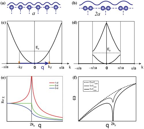
To understand the mechanism in Peierls’ picture, a simple model of free electron gas is usually employed to explain the transition. In a free electron gas model, the response of an electron gas to an external perturbation is described by the Lindhard response function χ0(q) that defines the stability of the electron system [Citation6]. In 1D, the real part of χ0(q) has a divergent singularity at q = 2kF, as shown in Figure (e), which means the 1D electron gas is unstable. In 1959, Kohn [Citation7] pointed out that there is an ‘Image of the Fermi Surface in the Vibrational Spectrum–’, because the zero energy electronic excitations at 2kF will effectively screen any lattice motion with this wave vector. Due to the divergence of χ0(q), the phonon mode, with a wave number close to 2kF, will be renormalized to have lower energy, which is called phonon softening. This strong renormalization of the phonon due to interactions with an electron system is referred to as the Kohn anomaly [Citation8]. The phonon renormalization is strongly temperature-dependent, with the phonon energy going to zero when the temperature decreases to Tc. This frozen phonon at Tc leads to a second-order phase transition into the CDW state [Citation1]. Figure (f) shows the ideal phonon dispersion of the 1D chain as a function of temperature. Below Tc the phonon energy at q = 2kF becomes imaginary, driving a new lattice structure. Above Tc there is a sharp dip in the phonon dispersion but no lattice restruction.
The Peierls’ picture was then extended to higher dimensions to explain the occurrence of CDWs based on the concept of Fermi surface nesting (FSN). One of the first cases where the term FSN was used in a 3D system was for the calculation of electronic structure of chromium [Citation9]. That is, if the particular topology of the Fermi surface allows matching segments of the Fermi surface upon translation by a fixed vector , a CDW state can be created with a spatial periodicity
. In this sense, the 1D metal has perfect FSN since the Fermi surface in 1D is just two fixed points at
.
Therefore, the key features of Peierls’ model include: FSN in electronic structure, a sharp peak in Lindhard function, Kohn anomaly in phonon spectra, a structural transition in lattice and a metal–insulator transition. These features are summarized in Table . But any real one-dimensional system is only quasi 1D, which may differentiate it from the ideal model. To experimentally confirm the features associated with a CDW state in real materials, transport measurements were routinely used in the early days to check the metal–insulator transition and reveal the transition temperature [Citation1]. Now a whole host of techniques can be utilized to fully characterize the features associated with a CDW. Angle resolved photoemission spectroscopy (ARPES) can determine the band structure and the Fermi contour [Citation10–12] that are needed to confirm FSN and calculate the susceptibility functions. Electron [Citation13,14], X-ray [Citation15], and neutron diffraction [Citation16,17] measurements can determine the structural transition. Scanning tunnelling microscopy (STM) and spectroscopy [Citation18,19] can determine the wave length of the charge modulation as well as the electronic transition. Inelastic neutron [Citation16,17], X-ray [Citation20], electron [Citation21] and helium atom [Citation21] scattering can probe the temperature dependence of the Kohn anomaly in the phonon dispersion. As an example, consider the quasi-1D material TTF-TCNQ, where many experimental techniques have been employed to study the physical properties [Citation22–27]. The results are summarized in Table and shown in Figure , indicating that all the features of a real quasi-1D material like TTF-TCNQ are consistent with the Peierls’ picture.
Table 1. Comparison of the key features of typical CDW materials with Peierls’ model.
Figure 2. Illustration of the CDW state of TTF-TCNQ. (a) STM image at 63 K showing the normal state. (b) STM image at 36 K showing the CDW state. Reprinted with permission from Ref. [Citation26]. Copyright (2003) by the American Physical Society. (c) ARPES intensity mapping at EF of TTF-TCNQ at 60 K, showing a clear 1D FSN. Reprinted with permission from Ref. [Citation27]. Copyright (2013) by the Physical Society of Japan. (d) Resistivity vs. temperature measurements showing a clear metal–insulator transition at 55 K [Citation22]. (e) Inelastic neutron scattering results of the acoustic phonon dispersion showing a strong Kohn anomaly [Citation25].
![Figure 2. Illustration of the CDW state of TTF-TCNQ. (a) STM image at 63 K showing the normal state. (b) STM image at 36 K showing the CDW state. Reprinted with permission from Ref. [Citation26]. Copyright (2003) by the American Physical Society. (c) ARPES intensity mapping at EF of TTF-TCNQ at 60 K, showing a clear 1D FSN. Reprinted with permission from Ref. [Citation27]. Copyright (2013) by the Physical Society of Japan. (d) Resistivity vs. temperature measurements showing a clear metal–insulator transition at 55 K [Citation22]. (e) Inelastic neutron scattering results of the acoustic phonon dispersion showing a strong Kohn anomaly [Citation25].](/cms/asset/1db3a3fc-126e-49a6-98fb-5503976e0603/tapx_a_1343098_f0002_oc.gif)
1.2. CDW in 2D: electron–phonon coupling
The challenge is to apply the Peierls’ picture of a CDW to materials in higher dimensions. As Peierls pointed out [Citation28]:
This (Peierls) instability came to me as a complete surprise when I was tidying material for my book (1955), and it took me a considerable time to convince myself that the argument was sound. It seemed of only academic significance, however, since there are no strictly one-dimensional systems in nature. I therefore did not think it worth publishing the argument, beyond a brief remark in the book, which did not even mention the logarithmic behaviour.
Peierls’ intuition might have been correct. In a layered quasi-2D material NbSe2, the classic and the most studied CDW system, a large number of studies [Citation18–20,29–32] have shown that the observed charge ordering phase transition is not truly analogues with the Peierls’ picture. Specifically, there is no indication of FSN. NbSe2 has a hexagonal layered structure with lattice constant of 3.443 Å. Early diffraction [Citation15,16] and recent STM measurements [Citation19] all confirmed the structural transition at TCDW = 33.5 K, with Å−1. Recent inelastic X-ray scattering [Citation20,33] revealed a Kohn-like anomaly in phonon spectra and showed that phonon softening located around
Å−1 induced the structural transition. However, the measured resistivity as a function of temperature showed no change at the CDW transition temperature [Citation34], indicating there is no metal–insulator transition associated with the structural transition. Most importantly, as shown in Figure (a), the Fermi contour obtained from ARPES measurements does not show any sign of FSN [Citation32]. The absence of FSN can be seen clearly in the plots of the Lindhard susceptibility function (real and imaginary) derived from the measured electronic structure, which shows no peak at the position of
, which will be discussed in detail in Section 2.
Figure 3. Origin of the CDW in NbSe2. (a) Fermi Surface Contours [Citation10] with the experimental [Citation16,17] shown. (b) Reχ(q) and (c) Imχ(q) calculated from experimental data [Citation10] along the ΓM direction. (d) Extracted EPC matrix element
[Citation32]. (e) Measured phonon dispersion (points) at T = 8 K [Citation20] and calculated soft phonon behaviour (solid line) using
and an approximation for the bare phonon (dashed line) dispersion [Citation32].
![Figure 3. Origin of the CDW in NbSe2. (a) Fermi Surface Contours [Citation10] with the experimental [Citation16,17] shown. (b) Reχ(q) and (c) Imχ(q) calculated from experimental data [Citation10] along the ΓM direction. (d) Extracted EPC matrix element [Citation32]. (e) Measured phonon dispersion (points) at T = 8 K [Citation20] and calculated soft phonon behaviour (solid line) using and an approximation for the bare phonon (dashed line) dispersion [Citation32].](/cms/asset/0dfb43a8-bb70-4c31-a93a-9bc37e08feb4/tapx_a_1343098_f0003_oc.gif)
All these features are summarized in Table to show the similarities and differences between NbSe2 and the ideal Peierls’ model. Apparently the origin of the CDW in this system is not driven by FSN. Instead, it has been postulated that CDW phases are dictated by the -dependent electron–phonon coupling (EPC) [Citation29–31,35]. Mazin and coworkers used the classical CDW materials NbSe2, TaSe2 and CeTe3 to show that with a proper inclusion of EPC the observed properties could be explained [Citation29–31]. One may argue that both FSN and EPC are forms of electron–lattice interaction, involving excitations of electrons from filled to empty states. However, they should be distinguished because FSN involves elastic scattering, whereas EPC involves inelastic scattering from the lattice [Citation32]. Recent experiments via phonon measurements have indeed confirmed the
-dependent EPC is the dominant origin of the CDW in NbSe2 [Citation20,33]. The details about EPC and Kohn anomaly will be discussed in Section 3.
Different from the quasi-2D layered materials, the surface can usually provide a platform for the formation of CDWs due to the breaking of translational symmetry. As summarized in Ref. [Citation36], the surface CDW transitions also appear to be system-dependent, and even the 1D CDW chains on the surface are different from the ideal Peierls’ picture. Nonetheless, some 2D metal films grown on semiconductor substrates such as Pb/Ge or Sn/Ge [Citation37–40], show surface CDW order with the origin according to theory consistent with the Peierls’ picture (also summarized in Table ). However, the experimental results on these systems are quite limited. More studies with state-of-the-art experimental techniques are needed to confirm the existence of a 2D Peierls’ CDW at a surface.
1.3. CDW with 3D character
The situation becomes more complicated when extending to 3D. CDW behaviour has been reported in several 3D systems, including the rare earth systems such as R5Ir4Si10 [Citation41,42], R2Ir3Si5 (R = Lu, Er) [Citation43,44], M3T4Sn13 (M = Ca, Sr; T = Ir, Rh) [Citation45–50] and IrTe2 [Citation51–59]. Although these systems usually have either quasi-1D chains or quasi-2D plains in the crystal structure, the strong interchain or interplanar interactions often lead to a three-dimensional character in their CDW states.
In the systems of R5Ir4Si10 and R2Ir3Si5, instead of a single CDW transition in the typical 1D or 2D cases, they usually show multiple CDW transitions [Citation42,44]. Moreover, different from regular CDW systems that usually show a second-order CDW phase transition, the CDW transition in these systems is first order [Citation41,44]. The CDW transitions in these materials are widely believed to be related to the existence of quasi-1D chains along one special crystallographic direction. But because of the 3D nature, the interchain couplings are very strong. Thus these systems may belong to a strong-coupling CDW class [Citation41]. The origin seems more complicated than typical low-dimensional CDW systems.
In the systems of M3T4Sn13, they exhibit a second-order structure transition (e.g. 35 K in Ca3Ir4Sn13 and 147 K in Sr3Ir4Sn13) coexisting with a superconducting transition (e.g. 7 K in Ca3Ir4Sn13 and 5 K in Sr3Ir4Sn13) [Citation45,50]. The structure transition was widely believed to take the systems into a 3D CDW state [Citation45,50]. Early studies attributed this CDW transition to the FSN picture [Citation45]. However, more recent optical spectroscopy studies found evidence for the presence of electron correlation effects and pointed to the unconventional strong-coupling CDW mechanism [Citation47]. However, the key experimental evidences, especially direct measurements of electronic structure and phonon dispersion of these materials have not been reported. Further studies are definitely needed to clarify the origin of the CDWs in these systems.
In the case of IrTe2, it exhibits a transition in the temperature range of 220–280 K with a large thermal hysteresis [Citation51], which is a signature of a first-order type structural transition from a 1 × 1 × 1 phase into a 5 × 1 × 5 phase, a structure with five times the periodicity in both the a and c directions. The existence of long-range ordering along the c direction means that there is significant interplanar coupling [Citation52], indicating the 3D character of this CDW phase. This behaviour was first thought to be a consequence of the partial gap opening due to a CDW transition [Citation51]. But no gap was observed in either ARPES [Citation53] or optical [Citation54] measurements. The orbital degrees of freedom are considered to play an important role to form the so-called orbital density wave [Citation51,55,56]. Recent studies suggest that Ir atoms form dimers during the structural phase transition [Citation57,58], which makes IrTe2 a rare system that has charge ordering (or charge disproportionation) and CDW-like lattice modulation coexisting in the metallic state [Citation59]. The first-order type phase transition with thermal hysteresis is possibly due to the interplay between the two mechanisms. But the origin of the CDW in this system is still not clear.
In summary, the complexity in 3D would make the mechanism of CDW much more complicated than the ideal 1D or 2D cases. The origin of CDWs in 3D is highly material-dependent, and may not be driven by a simple mechanism. Even more complicated is, electron correlation may play an important role in some 3D complex materials, as Overhauser discussed in his seminal paper [Citation60] about 3D simple metals. The details about the electron correlations will be discussed in Section 5.
1.4. CDW in cuprates
Another topic that is always mentioned when talking about CDW is its relationship with the formation of superconductivity. Although Fröhlich’s attempt [Citation3] to explain superconductivity by the movement of CDWs turned out to be incorrect, but the competition between CDW and superconductivity has emerged, especially after the discovery of unconventional superconductivity in cuprates since 1980s. Cuprates are often considered as quasi-2D layered materials. In cuprates, different charge ordering (CO) phenomena have been reported, such as a stripe phase in La1.6−xNd0.4SrxCuO4 [Citation61,62], a checker-board phase [Citation63,64] and a special kind of short-range CO phase [Citation5,65] in Bi2Sr2CaCu2O8+δ (Bi2212), and long-range charge fluctuations [Citation66] or CDWs [Citation67,68] in YBa2Cu3O6+x (YBCO). The competition between these CO phases and magnetic ordering and superconductivity [Citation69] continues to attract intensive interest in the community. As to the origin of the CO in cuprates, Comin et al. pointed out that the simple FSN near antinodal region is not the driving force of the CO [Citation70]. We have also shown that EPC in cuprates is not strong enough to drive the formation of CO, a Kohn anomaly, or CDW phase [Citation32]. Unlike the case in other quasi-2D layered materials like NbSe2, neither FSN nor EPC is directly relevant to the CO or CDW phases in cuprates. Actually, a recent STM study [Citation71] has clearly demonstrated that the observed modulations of the electronic structure in cuprates are unconventional density waves, where antiferromagnetic and Coulomb interactions may play a key role. What’s more complicated is, the 2D CDW in cuprates may give way to a 3D CDW at high magnetic field, as reported recently in YBCO [Citation72]. All these results suggest that electron correlations play a significant role in the formation of CO or CDW phase in cuprates. In any case, whatever the CO or CDW phase in cuprates is, it is not a conventional one. A good review about the CDWs in strongly correlated electron systems, especially in cuprate superconductors, is available in Ref. [Citation73].
1.5. Classification of CDWs based on their nature
As expected, the origin of CDW is strongly related to the dimensionality. The concept of a CDW has been applied to many materials without a clear definition of the origin of CDW. We have suggested that CDWs should be classified based on their nature [Citation32]. In our classification, there are at least three types of CDWs. Type I CDWs are quasi-1D systems with their origin in the Peierls’ instability (FSN), where the lattice distortion is a consequence of the electronic disturbance. The best example may be linear chain compounds. Type II CDWs are driven by EPC but not by FSN. Here the electronic and lattice instabilities are intimately tied to each other, and there is a phonon mode at , going to zero at the transition temperature TCDW. There is no reason to have a metal–insulator transition associated with the transition. A typical example of Type II is quasi-2D layered material NbSe2. Type III CDWs are systems where there is a charge modulation (or CO) with no indication of FSN or EPC as the driving force. The best example of Type III CDWs may be the cuprates that exhibit CO phenomena. Electron correlations probably play a significant role in these Type III systems.
There are already numerous comprehensive reviews (e.g. Refs. [Citation74–78]) about CDWs existing in literatures. In the following sections of this review, we summarize the properties of CDWs, where we try to describe and explain the possible existing misconceptions associated with the origin of CDWs in detail.
2. FSN and Lindhard function
Although FSN is a frequently used term in physics, there is always no rigorous definition about it in the literatures. It usually refers to a particular topology of the Fermi surface that allows matching segments of the Fermi surface upon translation by a fixed vector in momentum space. FSN means that there exist two parallel pieces of a Fermi surface, such that a single
vector can connect many points. Fermi surface with two seemingly parallel pieces may not be nested. The only way to determine the importance of nesting is to determine the Lindhard susceptibility function [Citation6].
To show the properties of Lindhard function, one needs to start with a theory of electron liquid [Citation79]. Here we review the derivations following the expressions from Ref. [Citation80].
If a system of electron liquid interacts with an external electric field with potential , where ω is the field frequency, the external field will cause an induced charge density
and an induced electrostatic potential
. Then the total potential is given by the sum of the external potential and the induced potential, i.e.
(1)
In a linear response theory, the induced charge density is linked to the total potential by a response function(2)
where is the density response function that contains the correlations between electrons at positions
and
. In momentum space this response function is expressed by
, which can be calculated using the random-phase approximation (RPA).
In the non-interacting Fermi Gas model, electron–electron correlations are ignored and the response function can be calculated via Lindhard approximation. The transition momentum is conserved with , and one of the momentum variables can be eliminated. Then, we obtain the Lindhard susceptibility function:
(3)
where ɛ is the electron’s energy, and f denotes the electron’s Fermi distribution function. Notice this is a complex function. The imaginary and real parts can be simplified as
(4)
and
(5)
For the special case of zero-energy transfer limit (or static limit), ω = 0, and . The Lindhard functions as a function of dimensionality are:
(6)
(7)
(8)
These results, corresponding to a free electron gas model, are plotted in Figure (e). The divergence of the real part in 1D defines a perfect FSN. In real materials, however, it is usually the case with ω ≠ 0. Thus, both the imaginary and real parts are critical to ‘act’ as a quantitative measure of the FSN. To define a FSN, a system must satisfy several requirements [Citation29]: (1) must has a peak at the CDW wave vector
; (2)
must also has a peak at
because the real part defines the stability of the electronic system; (3) The peak in
must translate into a divergence in the full electronic susceptibility to cause the electronic system to be unstable even without any ionic shifts. So a ‘real nesting’ requires peaks at
in both the imaginary and real parts of the Lindhard function, and the peaks should exist not only at zero frequency but also within some finite range of transition energies.
Experimentally, the imaginary part, , which is the function that reflects the FS topology, can be measured by neutron scattering. But the real part,
, which must diverge in order to trigger an electronic CDW, is difficult to directly obtain by experiments. Instead, with the development of ARPES, the full electronic structure can be experimentally mapped now. Then both
and
can be calculated from the measured electronic energy bands [Citation32].
When the electron–electron correlations are strong, the non-interacting Lindhard function cannot properly represent the properties of the electronic system. Ideally the interacting susceptibility or response function
, which carries the information from both electron–phonon and electron–electron interactions, should be used for the specific system being studied. However, experimentally it is not feasible to obtain the interacting
. In this case, if the Lindhard function
is calculated using the measured band structure, which contains both electron–phonon and electron–electron coupling as the input, it is an acceptable approximation to generate relatively close results [Citation32].
3. EPC and Kohn anomaly
In Peierls’ picture, the charge density transition is always accompanied with a lattice distortion. Usually, the CDW transition is described in a model that a free electron gas couples to the underlying lattice through EPC. In such a model, the EPC can be simplified and expressed by the Frohlich Hamiltonian [Citation3],(9)
The first term is the Hamiltonian for the free electron gas, with and
the creation and annihilation operators for electron states with energy
and wave vector
. The second term is the Hamiltonian for lattice vibrations, with
and
the creation and annihilation operators for phonons with energy
and wave vector
. The last term describes the EPC with a
-dependent coupling constant
.
The solution of this Hamiltonian generates the well-known EPC-induced phonon energy renormalization [Citation81]:
(10)
where is the renormalized phonon dispersion due to EPC,
is the bare phonon dispersion if EPC is absent and
is the interacting susceptibility function.
In a free electron gas model, the interacting can be approximated by the zero frequency limit of the non-interacting Lindhard function
. And traditionally,
is assumed to be a
-independent constant [Citation1]. Then using the results of Equations (6), (7) and (8), one can immediately see that the phonon energy at
is considerably lowered for a metal in any dimension. This phenomenon was first proposed by Walter Kohn in 1959 [Citation7], and thus is called Kohn anomaly in phonon dispersions [Citation8].
Kohn anomaly is usually considered as a consequence of the structure in the response function. Especially in the case of FSN, as mentioned above, is divergent at the nesting vector. Then the renormalized energy of the phonon becomes imaginary [
], meaning that a static lattice distortion appears, which corresponds to the CDW transition in Peierls’ picture. The detailed derivations about Kohn anomaly and the CDW transition are described in Gruner’s book [Citation1].
As introduced in Section 1, in real 2D materials, there is often no FSN. For instance, in the case of NbSe2, is not divergent at the CDW vector. Actually, there are no peaks at all at
in both
and
in NbSe2, as shown in Figure (b) and (c), respectively. However, there is a Kohn-like anomaly in the acoustic phonon dispersion [Citation20]. So the assumption that
is
-independent is not always correct. In the case of NbSe2,
is not only strongly
-dependent, but also strongly anisotropic. Along ΓM direction, as shown in Figure (d),
has an obvious peak at
. As illustrated in Figure (e), this peak in
can effectively lower the energy of the acoustic phonon to zero, and thus drive the lattice distortion.
Strong EPC usually softens the corresponding phonon energy, but does not necessarily lead to a strong Kohn anomaly to drive the lattice distortion. For example, in the case of Bi2212, a typical quasi-2D cuprate, the optical A1g phonon branch at ~80 meV shows a rapid downward dispersion (Figure (a)) accompanied with increasing linewidth (Figure (b)) for momentum larger than ~0.41 Å−1, indicating a large EPC for this A1g phonon mode. The EPC matrix element of this mode is calculated using published ARPES data that determines
[Citation82] and the fit to the reported phonon dispersion and linewidth [Citation83], as shown in Figure (c). Notice that the maximum value of
is similar for both NbSe2 and Bi2212. Different from the case of NbSe2, the peak in
of Bi2212 is at the BZ boundary, which if large enough in magnitude would have driven the phonon energy imaginary, resulting in a commensurate reconstruction, i.e. a
superstructure which has been reported for Sr2RuO4 when a phonon goes soft at the zone boundary [Citation84]. In fact, however, although
is large, the oxygen A1g phonon mode in Bi2212 does not go to zero because its energy is also quite large [Citation32].
Figure 4. EPC associated with apical oxygen A1g phonon mode in optimally doped Bi2Sr2CaCu2O8+δ [Citation32]. (a) Fit to the measured phonon dispersion [Citation83] as a function of momentum. (b) Fit to the measured linewidth as a function of momentum. (c) extracted from the phonon [Citation83] and ARPES [Citation82] data.
![Figure 4. EPC associated with apical oxygen A1g phonon mode in optimally doped Bi2Sr2CaCu2O8+δ [Citation32]. (a) Fit to the measured phonon dispersion [Citation83] as a function of momentum. (b) Fit to the measured linewidth as a function of momentum. (c) extracted from the phonon [Citation83] and ARPES [Citation82] data.](/cms/asset/f17537b2-baec-4567-a5fb-bebdd5cccc54/tapx_a_1343098_f0004_oc.gif)
4. Structural transition and metal–insulator transition
In Peierls’ picture, as shown in Table , a CDW transition is always accompanied with a structural transition in lattice as well as a metal–insulator transition as a consequence of opening a gap at the Fermi level. Measurements of the transport properties can give evidence of the metal–insulator transition and reveal the transition temperature. However, in real materials, the transport properties are much more complicated than the theoretical models. Not all CDW materials show obvious signatures of metal–insulator transition in the transport measurements. In this sense, metal–insulator transition should not be regarded as a necessary characteristic of CDW.
In Figure , we show the resistivity as a function of temperature for three typical CDW materials. In the case of a 1D TTF-TCNQ (Figure (a)), it shows a clear metal–insulator transition at TC = 55 K [Citation22]. But in the case of another quasi-1D system NbSe3 (Figure (b)) there is no clear metal–insulator transition at TC. Instead, there are two anomalies at 149 and 59 K [Citation85], corresponding to two phase transitions from different atomic chains [Citation86]. The system remains metallic after the transition, since NbSe3 is not a real 1D system [Citation87,88], so the phase transition opens a gap only in part of the Fermi surface along certain direction, i.e. it is not really 1D. There is no gap on other parts of the Fermi surface due to the anisotropic electronic structure [Citation88].
Figure 5. Resistivity vs. temperature measurements for typical CDW materials. (a) 1D chain TTF-TCNQ [Citation22]. (b) 1D chain NbSe3 [Citation85]. (c) 2D layered NbSe2 [Citation34].
![Figure 5. Resistivity vs. temperature measurements for typical CDW materials. (a) 1D chain TTF-TCNQ [Citation22]. (b) 1D chain NbSe3 [Citation85]. (c) 2D layered NbSe2 [Citation34].](/cms/asset/834c0b08-3c5f-42ee-8978-6730aac4b46c/tapx_a_1343098_f0005_oc.gif)
In the classic 2D CDW system, NbSe2 (Figure (c)), there is no signature of metal–insulator transition at all [Citation34]. No CDW induced energy gap was observed in this material until 2009 when small anisotropic energy gaps were measured [Citation12]. However, the precise magnitude and wave vectors of the gaps are still controversial [Citation20]. Obviously, the measured gaps are so small and only present in certain points on the Fermi surface, thus the transport properties are not affected by these gaps.
The phase transitions associated with CDW are really system-dependent. There is no universal mechanism that is applicable to all materials. And usually the mechanism of the transition is much more complicated than the ideal Peierls’ model. Understanding the details of the structural transition as well as the anisotropic electronic structure is a prerequisite to explore the origin of the phase transitions observed in the transport measurements.
5. Electron correlations: Overhauser’s theory
All the discussions above about CDW are from the origin of Peierls’ picture, in which electron–lattice interaction is always the starting point. Actually there is another independent approach, Overhauser’s CDW theory, from the point of view of exchange and correlation interactions among electrons.
In Overhauser’s theory, CDW and SDW are closely related [Citation89–91]. Due to the exchange and correlation interactions among itinerant electrons, there are non-uniform states (called ‘exchange-instability wave’ in Overhauser’s paper [Citation60]) in which the charge density or the spin density (or both) exhibit spatial oscillations at a wave vector close in magnitude to 2kF. The spin-up and spin-down densities are
(11)
where ρ0 is the mean electron density, p is fractional modulation of the wave and φ is the relative phase of the spin-up and spin-down density oscillations. For φ = 0 it defines a pure CDW with uniform spin density, while for it describes a pure SDW with uniform charge density. The values with
describes mixed CDW-SDW states.
In early 1960s, Overhauser [Citation90,91] proved that ‘within the Hartree-Fock approximation, the homogeneous paramagnetic states of the three-dimensional electron gas is unstable with respect to the formation of spin- or charge-modulated states’. In 1968, Overhauser went on to argue that correlations will likely to decrease the energy of the CDW states relative to that of the SDW by a displacement of the positive ions from their normal equilibrium sites [Citation60]. Or in another word, electric fields caused by a CDW will displace the positive ions from their ideal equilibrium sites . The displacements can be expressed as
(12)
and can be regarded as a static modulation of the lattice.
This means that the correlations favour density modulations over spin modulations, which gives a surprising conclusion [Citation60] that CDW instabilities can occur in a simple metal, such as potassium (K) in particular.
It should be noted that Overhauser’s idea about CDW is really different from the ones evolved out of Peierls’ picture that we have reviewed in above sections. Overhauser’s CDW state would occur in a system that has an essentially spherical Fermi surface (a 3D metal) to begin with [Citation79], while the CDWs evolved out of Peierls’ picture usually require anisotropic Fermi surface or EPC in lower dimensions.
Overhauser has been able to produce an impressive list of experimental facts that suggest the existence of a CDW ground state in potassium. Although several of them have been implicitly supported by some experiments [Citation79], the key features to prove the existence of a CDW in potassium such as satellite peaks in diffraction measurements [Citation92] have not been observed till now. Nevertheless, the Overhauser’s prediction is of great significance that shows the important role of electron correlations in the CDWs of some complex materials. Indeed, in a classical CDW system TiSe2, although the origin of the CDW transition is still under intense debate [Citation93,94], a large amount of experiments point to the prominent role of electron correlations [Citation95–97]. The CDW state is even referred to as ‘Overhauser type’ in some references [Citation93,95]. Recently, a CDW state discovered on the surface of K0.9Mo6O17 was also believed to be driven by electron correlations [Citation98]. Moreover, electron correlation also supplies some basic ideas that might be helpful to understand the elusive mechanism of all kinds of CO phases in systems, say for example, cuprates [Citation69,99,100].
6. Summary
CDW is an extremely important concept in condensed matter physics. However, the origin of CDW is much more complicated than the descriptions in any existing textbook. The concept of a CDW has been applied to many materials without a clear definition of the origin of CDW, and several terms related to CDW such as FSN also lack rigorous definitions. As a result, misconceptions about CDW can sometimes be seen in the literatures, which will confuse or even mislead the readers, especially students or researchers who are new to the field. We try to summarize and explain the concepts associated with the origin of CDW in detail in this simple review. We hope this review will be helpful to the students or researchers that start to comprehend the concepts.
Funding
X.Z. was supported by the Youth Innovation Promotion Association of CAS. J.G. was supported by NSF of China through grant number 11634016. J.Z. was supported by U.S. NSF through grant number DMR-16088865. E.W.P was supported by U.S. NSF through grant number DMR-1504226.
Disclosure statement
No potential conflict of interest was reported by the authors.
References
- G. Gruner, Density Waves in Solids, Vol. 89, Addison-Wesley Publishing Company, Massachusetts, 1994.
- R.E. Peierls, Quantum Theory of Solids, Oxford University, New York, 1955.
- H. Frohlich, Proc. R. Soc. Lon. Ser-A 223 (1954) p.296.10.1098/rspa.1954.0116
- J. Bardeen, L.N. Cooper and J.R. Schrieffer, Phys. Rev. 108 (1957) p.1175.10.1103/PhysRev.108.1175
- E.H. da Silva Neto, P. Aynajian, A. Frano, R. Comin, E. Schierle, E. Weschke, A. Gyenis, J. Wen, J. Schneeloch, Z. Xu, S. Ono, G. Gu, M. Le Tacon and A. Yazdani, Science 343 (2014) p.393.10.1126/science.1243479
- J. Lindhard, Mat. Fys. Medd. Dan. Vid. 28 (1954) p.1.
- W. Kohn, Phys. Rev. Lett. 2 (1959) p.393.10.1103/PhysRevLett.2.393
- E.J. Woll and W. Kohn, Phys. Rev. 126 (1962) p.1693.10.1103/PhysRev.126.1693
- W.M. Lomer, P. Phys. Soc. Lond. 80 (1962) p.489.10.1088/0370-1328/80/2/316
- D.S. Inosov, V.B. Zabolotnyy, D.V. Evtushinsky, A.A. Kordyuk, B. Buchner, R. Follath, H. Berger and S.V. Borisenko, New J. Phys. 10 (2008) p.12507.
- S.V. Borisenko, A.A. Kordyuk, A.N. Yaresko, V.B. Zabolotnyy, D.S. Inosov, R. Schuster, B. Buchner, R. Weber, R. Follath, L. Patthey and H. Berger, Phys. Rev. Lett. 100 (2008) p.196402.
- S.V. Borisenko, A.A. Kordyuk, V.B. Zabolotnyy, D.S. Inosov, D. Evtushinsky, B. Buchner, A.N. Yaresko, A. Varykhalov, R. Follath, W. Eberhardt, L. Patthey and H. Berger, Phys. Rev. Lett. 102 (2009) p.166402.10.1103/PhysRevLett.102.166402
- O. Singh and A. Curzon, Phys. Lett. A 56 (1976) p.63.10.1016/0375-9601(76)90031-1
- C. Chen, Solid State Commun. 49 (1984) p.645.10.1016/0038-1098(84)90211-4
- C.H. Du, W.J. Lin, Y. Su, B.K. Tanner, P.D. Hatton, D. Casa, B. Keimer, J.P. Hill, C.S. Oglesby and H. Hohl, J. Phys-Condens. Mat. 12 (2000) p.5361.10.1088/0953-8984/12/25/302
- D.E. Moncton, J.D. Axe and F.J. DiSalvo, Phys. Rev. Lett. 34 (1975) p.734.10.1103/PhysRevLett.34.734
- D.E. Moncton, J.D. Axe and F.J. DiSalvo, Phys. Rev. B 16 (1977) p.801.10.1103/PhysRevB.16.801
- A. Soumyanarayanan, M.M. Yee, Y. He, J. van Wezel, D.J. Rahn, K. Rossnagel, E.W. Hudson, M.R. Norman and J.E. Hoffman, Proc. Natl. Acad. Sci. U.S.A. 110 (2013) p.1623.10.1073/pnas.1211387110
- C.J. Arguello, S.P. Chockalingam, E.P. Rosenthal, L. Zhao, C. Gutierrez, J.H. Kang, W.C. Chung, R.M. Fernandes, S. Jia, A.J. Millis, R.J. Cava and A.N. Pasupathy, Phys. Rev. B 89 (2014) p.235115.
- F. Weber, S. Rosenkranz, J.P. Castellan, R. Osborn, R. Hott, R. Heid, K.P. Bohnen, T. Egami, A.H. Said and D. Reznik, Phys. Rev. Lett. 107 (2011) p.107403.10.1103/PhysRevLett.107.107403
- J. Toennies, Experimental Determination of Surface Phonons by Helium atom and Electron Energy Loss Spectroscopy, in Surface Phonons, W. Kress, F. W. d. W., ed. Springer, Berlin, 1991, p.111.
- C.W. Chu, J.M.E. Harper, T.H. Geballe and R.L. Greene, Phys. Rev. Lett. 31 (1973) p.1491.10.1103/PhysRevLett.31.1491
- L.B. Coleman, M.J. Cohen, D.J. Sandman, F.G. Yamagishi, A.F. Garito and A.J. Heeger, Solid State Commun. 12 (1973) p.1125.10.1016/0038-1098(73)90127-0
- R. Comes, S. Shapiro, G. Shirane, A. Garito and A. Heeger, Phys. Rev. Lett. 35 (1975) p.1518.10.1103/PhysRevLett.35.1518
- H. Mook and C.R. Watson Jr, Phys. Rev. Lett. 36 (1976) p.801.10.1103/PhysRevLett.36.801
- Z. Wang, J. Girard, C. Pasquier, D. Jérome and K. Bechgaard, Phys. Rev. B 67 (2003) p.121401.10.1103/PhysRevB.67.121401
- K. Koizumi, K. Ishizaka, T. Kiss, M. Okawa, R. Kato and S. Shin, J. Phys. Soc. Jpn. 82 (2013) p.025004.10.7566/JPSJ.82.025004
- R.E. Peierls, More Surprises in Theoretical Physics, Princeton: New Jersey, 1991.
- M.D. Johannes and I.I. Mazin, Phys Rev B 77 (2008) p.165135.
- M.D. Johannes, I.I. Mazin and C.A. Howells, Phys. Rev. B 73 (2006) p.205102.10.1103/PhysRevB.73.205102
- M. Calandra, I.I. Mazin and F. Mauri, Phys. Rev. B 80 (2009) p.241108.10.1103/PhysRevB.80.241108
- X.T. Zhu, Y.W. Cao, J.D. Zhang, E.W. Plummer and J.D. Guo, Proc. Natl. Acad. Sci. U.S.A. 112 (2015) p.2367.10.1073/pnas.1424791112
- F. Weber, R. Hott, R. Heid, K.P. Bohnen, S. Rosenkranz, J.P. Castellan, R. Osborn, A.H. Said, B.M. Leu and D. Reznik, Phys. Rev. B 87 (2013) p.245111.
- M. Naito and S. Tanaka, J. Phys. Soc. Jpn. 51 (1982) p.219.10.1143/JPSJ.51.219
- C. Varma and A. Simons, Phys. Rev. Lett. 51 (1983) p.138.10.1103/PhysRevLett.51.138
- P.C. Snijders and H.H. Weitering, Rev. Mod. Phys. 82 (2010) p.307.10.1103/RevModPhys.82.307
- J.M. Carpinelli, H.H. Weitering, E.W. Plummer and R. Stumpf, Nature 381 (1996) p.398.10.1038/381398a0
- J.M. Carpinelli, H.H. Weitering, M. Bartkowiak, R. Stumpf and E.W. Plummer, Phys. Rev. Lett. 79 (1997) p.2859.10.1103/PhysRevLett.79.2859
- R. Perez, J. Ortega and F. Flores, Phys. Rev. Lett. 86 (2001) p.4891.10.1103/PhysRevLett.86.4891
- D. Farias, W. Kaminski, J. Lobo, J. Ortega, E. Hulpke, R. Perez, F. Flores and E.G. Michel, Phys. Rev. Lett. 91 (2003) p.016103.
- B. Becker, N.G. Patil, S. Ramakrishnan, A.A. Menovsky, G.J. Nieuwenhuys, J.A. Mydosh, M. Kohgi and K. Iwasa, Phys. Rev. B 59 (1999) p.7266.10.1103/PhysRevB.59.7266
- F. Galli, S. Ramakrishnan, T. Taniguchi, G.J. Nieuwenhuys, J.A. Mydosh, S. Geupel, J. Lüdecke and S. van Smaalen, Phys. Rev. Lett. 85 (2000) p.158.10.1103/PhysRevLett.85.158
- Y. Singh, D. Pal, S. Ramakrishnan, A.M. Awasthi and S.K. Malik, Phys. Rev. B 71 (2005) p.045109.10.1103/PhysRevB.71.045109
- N.S. Sangeetha, A. Thamizhavel, C.V. Tomy, S. Basu, A.M. Awasthi, P. Rajak, S. Bhattacharyya, S. Ramakrishnan and D. Pal, Phys. Rev. B 91 (2015) p.205131.
- L.E. Klintberg, S.K. Goh, P.L. Alireza, P.J. Saines, D.A. Tompsett, P.W. Logg, J. Yang, B. Chen, K. Yoshimura and F.M. Grosche, Phys. Rev. Lett. 109 (2012) p.237008.10.1103/PhysRevLett.109.237008
- S.K. Goh, D.A. Tompsett, P.J. Saines, H.C. Chang, T. Matsumoto, M. Imai, K. Yoshimura and F.M. Grosche, Phys. Rev. Lett. 114 (2015) p.097002.10.1103/PhysRevLett.114.097002
- A.F. Fang, X.B. Wang, P. Zheng and N.L. Wang, Phys. Rev. B. 90 (2014) p.035115.
- C.N. Kuo, C.W. Tseng, C.M. Wang, C.Y. Wang, Y.R. Chen, L.M. Wang, C.F. Lin, K.K. Wu, Y.K. Kuo and C.S. Lue, Phys. Rev. B 91 (2015) p.165141.
- D.G. Mazzone, S. Gerber, J.L. Gavilano, R. Sibille, M. Medarde, B. Delley, M. Ramakrishnan, M. Neugebauer, L.P. Regnault, D. Chernyshov, A. Piovano, T.M. Fernandez-Diaz, L. Keller, A. Cervellino, E. Pomjakushina, K. Conder and M. Kenzelmann, Phys. Rev. B 92 (2015) p.024101.
- K.F. Wang and C. Petrovic, Phys. Rev. B 86 (2012) p.024522.
- J.J. Yang, Y.J. Choi, Y.S. Oh, A. Hogan, Y. Horibe, K. Kim, B.I. Min and S.W. Cheong, Phys. Rev. Lett. 108 (2012) p.116402.10.1103/PhysRevLett.108.116402
- C. Chen, J. Kim, Y.F. Yang, G.X. Cao, R.Y. Jin and E.W. Plummer, Phys. Rev. B 95 (2017) p.094118.
- D. Ootsuki, S. Pyon, K. Kudo, M. Nohara, M. Horio, T. Yoshida, A. Fujimori, M. Arita, H. Anzai, H. Namatame, M. Taniguchi, N.L. Saini and T. Mizokawa, J. Phys. Soc. Jpn. 82 (2013) p.093704.10.7566/JPSJ.82.093704
- A.F. Fang, G. Xu, T. Dong, P. Zheng and N.L. Wang, Sci. Rep. 3 (2013) p.1153.10.1038/srep01153
- S. Pyon, K. Kudo and M. Nohara, J. Phys. Soc. Jpn. 81 (2012) p.053701.10.1143/JPSJ.81.053701
- D. Ootsuki, Y. Wakisaka, S. Pyon, K. Kudo, M. Nohara, M. Arita, H. Anzai, H. Namatame, M. Taniguchi, N.L. Saini and T. Mizokawa, Phys. Rev. B 86 (2012) p.014519.10.1103/PhysRevB.86.014519
- G.L. Pascut, K. Haule, M.J. Gutmann, S.A. Barnett, A. Bombardi, S. Artyukhin, T. Birol, D. Vanderbilt, J.J. Yang, S.W. Cheong and V. Kiryukhin, Phys. Rev. Lett. 112 (2014) p.086402.10.1103/PhysRevLett.112.086402
- J. Dai, K. Haule, J.J. Yang, Y.S. Oh, S.W. Cheong and W. Wu, Phys. Rev. B 90 (2014) p.235121.10.1103/PhysRevB.90.235121
- K. Kim, S. Kim, K.T. Ko, H. Lee, J.H. Park, J.J. Yang, S.W. Cheong and B.I. Min, Phys. Rev. Lett. 114 (2015) p.136401.10.1103/PhysRevLett.114.136401
- A.W. Overhauser, Phys. Rev. 167 (1968) p.691.10.1103/PhysRev.167.691
- J. Tranquada, B. Sternlieb, J. Axe, Y. Nakamura and S. Uchida, Nature 375 (1995) p.561.10.1038/375561a0
- S.A. Kivelson, I.P. Bindloss, E. Fradkin, V. Oganesyan, J.M. Tranquada, A. Kapitulnik and C. Howald, Rev. Mod. Phys. 75 (2003) p.1201.10.1103/RevModPhys.75.1201
- J. Hoffman, E. Hudson, K. Lang, V. Madhavan, H. Eisaki, S. Uchida and J. Davis, Science 295 (2002) p.466.10.1126/science.1066974
- W. Wise, M. Boyer, K. Chatterjee, T. Kondo, T. Takeuchi, H. Ikuta, Y. Wang and E. Hudson, Nat. Phys. 4 (2008) p.696.10.1038/nphys1021
- M. Hashimoto, G. Ghiringhelli, W.S. Lee, G. Dellea, A. Amorese, C. Mazzoli, K. Kummer, N.B. Brookes, B. Moritz, Y. Yoshida, H. Eisaki, Z. Hussain, T.P. Devereaux, Z.X. Shen and L. Braicovich, Phys. Rev. B 89 (2014) p.220511(R).
- G. Ghiringhelli, M. Le Tacon, M. Minola, S. Blanco-Canosa, C. Mazzoli, N. Brookes, G. De Luca, A. Frano, D. Hawthorn and F. He, Science 337 (2012) p.821.10.1126/science.1223532
- J. Chang, E. Blackburn, A. Holmes, N. Christensen, J. Larsen, J. Mesot, R. Liang, D. Bonn, W. Hardy and A. Watenphul, Nat. Phys. 8 (2012) p.871.10.1038/nphys2456
- E. Blackburn, J. Chang, M. Hücker, A. Holmes, N. Christensen, R. Liang, D. Bonn, W. Hardy, U. Rütt and O. Gutowski, Phys. Rev. Lett. 110 (2013) p.137004.10.1103/PhysRevLett.110.137004
- A. Gabovich, A. Voitenko, T. Ekino, M.S. Li, H. Szymczak and M. Pękała, Adv. Cond. Matter Phys. 2010 (2010) p.681070.
- R. Comin, A. Frano, M. Yee, Y. Yoshida, H. Eisaki, E. Schierle, E. Weschke, R. Sutarto, F. He and A. Soumyanarayanan, Science 343 (2014) p.390.10.1126/science.1242996
- K. Fujita, M.H. Hamidian, S.D. Edkins, C.K. Kim, Y. Kohsaka, M. Azuma, M. Takano, H. Takagi, H. Eisaki, S.-I. Uchida, A. Allais, M.J. Lawler, E.-A. Kim, S. Sachdev and J.C.S. Davis, Proc. Natl. Acad. Sci. 111 (2014) p.E3026.10.1073/pnas.1406297111
- S. Gerber, H. Jang, H. Nojiri, S. Matsuzawa, H. Yasumura, D.A. Bonn, R. Liang, W.N. Hardy, Z. Islam, A. Mehta, S. Song, M. Sikorski, D. Stefanescu, Y. Feng, S.A. Kivelson, T.P. Devereaux, Z.X. Shen, C.C. Kao, W.S. Lee, D. Zhu and J.S. Lee, Science 350 (2015) p.949.10.1126/science.aac6257
- C.-W. Chen, J. Choe and E. Morosan, Rep. Prog. Phys. 79 (2016) p.084505.10.1088/0034-4885/79/8/084505
- J.A. Wilson, F.J. Disalvo and S. Mahajan, Adv. Phys. 24 (1975) p.117.10.1080/00018737500101391
- G. Gruner, Rev. Mod. Phys. 60 (1988) p.1129.10.1103/RevModPhys.60.1129
- R.E. Thorne, Phys. Today 49 (1996) p.42.10.1063/1.881498
- P. Monceau, Adv. Phys. 61 (2012) p.325.10.1080/00018732.2012.719674
- K. Rossnagel, J. Phys-Condens. Mat. 23 (2011) p.213001.
- G. Giuliani and G. Vignale, Quantum Theory of the Electron Liquid, Cambridge University Press, Cambridge, 2005.10.1017/CBO9780511619915
- B. Mihaila, arXiv preprint arXiv: 1111.5337 (2011).
- G. Grimvall, The Electron-phonon Interaction in Metals, North-Holland Publishing Company, Amsterdam, 1981.
- M.R. Norman, M. Randeria, H. Ding and J.C. Campuzano, Phys. Rev. B 52 (1995) p.615.10.1103/PhysRevB.52.615
- H.J. Qin, J.R. Shi, Y.W. Cao, K.H. Wu, J.D. Zhang, E.W. Plummer, J. Wen, Z.J. Xu, G.D. Gu and J.D. Guo, Phys. Rev. Lett. 105 (2010) p.256402.10.1103/PhysRevLett.105.256402
- R. Matzdorf, Z. Fang, J. Zhang, T. Kimura, Y. Tokura, K. Terakura and E. Plummer, Science 289 (2000) p.746.10.1126/science.289.5480.746
- J. Chaussy, P. Haen, J.C. Lasjaunias, P. Monceau, G. Waysand, A. Waintal, A. Meerschaut, P. Molinié and J. Rouxel, Solid State Commun. 20 (1976) p.759.10.1016/0038-1098(76)90289-1
- J.L. Hodeau, M. Marezio, C. Roucau, R. Ayroles, A. Meerschaut, J. Rouxel and P. Monceau, J. Phys. C. Solid State 11 (1978) p.4117.10.1088/0022-3719/11/20/009
- A.H. Moudden, J.D. Axe, P. Monceau and F. Levy, Phys. Rev. Lett. 65 (1990) p.223.10.1103/PhysRevLett.65.223
- C.W. Nicholson, C. Berthod, M. Puppin, H. Berger, M. Wolf, M. Hoesch and C. Monney, Phys. Rev. Lett. (2017) p.206401.
- A.W. Overhauser, J. Phys. Chem. Solids 13 (1960) p.71.10.1016/0022-3697(60)90128-1
- A. Overhauser, Phys. Rev. Lett. 4 (1960) p.462.10.1103/PhysRevLett.4.462
- A. Overhauser, Phys. Rev. 128 (1962) p.1437.10.1103/PhysRev.128.1437
- A. Overhauser, Phys. Rev. B 3 (1971) p.3173.10.1103/PhysRevB.3.3173
- M. Calandra and F. Mauri, Phys. Rev. Lett. 106 (2011) p.196406.
- Y.I. Joe, X.M. Chen, P. Ghaemi, K.D. Finkelstein, G.A. de la Pena, Y. Gan, J.C.T. Lee, S. Yuan, J. Geck, G.J. MacDougall, T.C. Chiang, S.L. Cooper, E. Fradkin and P. Abbamonte, Nat. Phys. 10 (2014) p.421.10.1038/nphys2935
- G. Li, W.Z. Hu, D. Qian, D. Hsieh, M.Z. Hasan, E. Morosan, R.J. Cava and N.L. Wang, Phys. Rev. Lett. 99 (2007) p.027404.
- Z.Y. Zhu, Y.C. Cheng and U. Schwingenschlogl, Phys. Rev. B 85 (2012)p.245133.
- L.J. Li, E.C.T. O’Farrell, K.P. Loh, G. Eda, B. Ozyilmaz and A.H.C. Neto, Nature 529 (2016) p.185.
- D. Mou, A. Sapkota, H.H. Kung, V. Krapivin, Y. Wu, A. Kreyssig, X. Zhou, A.I. Goldman, G. Blumberg, R. Flint and A. Kaminski, Phys. Rev. Lett. 116 (2016) p.196401.10.1103/PhysRevLett.116.196401
- T. Ekino, A.M. Gabovich, M.S. Li, M. Pekala, H. Szymczak and A.I. Voitenko, J. Phys-Condens. Mat. 23 (2011) p.699.
- R.S. Markiewicz, I.G. Buda, P. Mistark, C. Lane and A. Bansil, Sci. Rep. 7 (2017) p.44008.