
 ?Mathematical formulae have been encoded as MathML and are displayed in this HTML version using MathJax in order to improve their display. Uncheck the box to turn MathJax off. This feature requires Javascript. Click on a formula to zoom.
ABSTRACT
A new research field of functional materials and device physics is rising that combines ionic transport with charge carrier modulation to realize emergent physical properties and discovery of metastable phases. The paradigm for enabling function extends far beyond carrier accumulation or depletion in band semiconductors or simply moving ions through an insulating electrolyte. Rather, by carefully selecting electronically or structurally fragile materials, one can collapse or open band gaps via extreme ionic dopant concentration, or reconfigure their entire crystal structure to create new phases. Electron–electron and electron–lattice interactions can be coupled or controlled independently in such systems via electric fields without thermal constraints by use of ionic dopants. The unifying theme across these studies is to introduce ions and electrons via electric fields through interfaces, with electrochemistry playing a dominant role. In this review, we briefly summarize this nascent field of iontronics and discuss principal results to date with examples from binary and complex oxides as well as selected 2D materials systems. We conclude the review by highlighting gaps in fundamental scientific understanding and prospects for the use of such novel devices in future electronic, photonic and energy technologies.
Graphical Abstract
1 Ion-electron doping of complex materials
Control over the structure and composition of materials at the atomic scale is paramount in condensed matter physics and materials sciences. Solid state electronic and photonic devices pioneered since the 20th century (e.g. transistors and lasers) typically comprise precisely engineered semiconductors and heterostructures, and function is achieved by manipulating the position of Fermi level with respect to the band edges. External fields are used to control band bending while the band gap does not change significantly. In the field of ionic materials and devices (e.g. battery electrolytes), however, function is achieved by chemical modification of the entire material with little regard for Thomas-Fermi screening length, either through redox processes, interfacial gas–solid/solid–liquid interactions, or ion transport under chemical potential gradient.
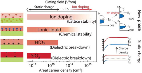
In this review, we describe an emerging field where reversible changes in the structural and electronic properties of a material can be achieved with electric fields by moving ions into or out of a material. Electron-ion coupling is exploited to bridge the gap between traditional fields that separately focus on electrons or ions [Citation1,Citation2,Citation3,Citation4,Citation5,Citation6,Citation7]. ), shows the carrier concentration manipulation strategies transforming from traditional static charge gating to ion doping (electron-ion coupling). While areal carrier density modulation is possible with traditional solid gate dielectrics (e.g. silica and hafnia) and electric double layers with ionic liquids or gels, the extent of carrier density modulation is limited. In the case of gate insulators, such limit is set by combination of dielectric breakdown strength and band offset that is spatially limited to the electrostatic screening length. In case of ionic liquids, the extent of carrier density modulation is restricted by the chemical stability of the ionic liquid-semiconductor interface and hence can vary drastically depending on the specific system. On the other hand, ion doping is not limited to screening length limitations since it is diffusive. Additionally, electrostatic modulation is volatile, while ion doping may have controllable volatility depending on the binding strength of the dopant to the lattice. The schematic on the far right of ) shows that band bending is responsible for carrier density modulation in electrostatic doping, while in the case of ion doping, the extremely high carrier densities can lead to complete reconstruction of the electronic band structures.
Figure 1. Mechanisms and function realization in electrostatic and ion doping processes. (a) Left and middle columns: schematic of methods and the carrier modulation capabilities of electrostatic gating and ion doping. Right column: electrostatic gating methods modestly change electronic band structure through band bending, while ion doping can result in band structure reconstruction. (b) Ion doping can be used to tune the properties of materials through structural, orbital, charge and spin degrees of freedom. (c) Functionalities that can be tuned by ion doping, and potential relevance to electronics, energy and emerging applications.
As shown in ), doping a material with ions can not only modify the lattice and produce structural phase transformations at high ion concentration, [Citation4,Citation8,Citation9] but also drastically change electronic properties [Citation6,Citation10–Citation16]. The dopant can be inserted from an external reservoir through diffusion or by applying an electric field gradient, while inherent instability may enable the material to selectively lose ions from one sub-lattice preferentially. For instance, ion-electron doping can change band filling in the electronic structure and therefore modify the conductivity of a material [Citation17]. Such conductivity modulation can also be achieved through changes in the bandwidth due to structural modifications [Citation18]. In addition, the magnetic properties of materials can be altered through reversible ion doping mediated by electric fields [Citation6,Citation7,Citation16,Citation19]. In ), we present various emerging technologies utilizing ion doping-induced functionalities. They are categorized into three major areas: electronics, energy, and emerging applications. The different functionalities and applications are discussed below and are labeled in the outer ring of ).
There have been experimental reports demonstrating the tunability of physical and chemical properties of materials by ion doping, as illustrated in . Hydrogen doping for instance can induce orders of magnitude changes to the electrical conductivity of the perovskite nickelates via a doping-induced Mott transition – a quantum mechanical effect-driven phase change [Citation4,Citation20]. Oxide materials like strontium cobaltite and two-dimensional bismuth chalcogenides can switch from optically transparent to opaque states by ion intercalation [Citation3,Citation21]. By tuning of magnetic anisotropy and spin orbital coupling, ion doping can manipulate the magneto-optical or current-induced magnetic switching behaviors [Citation22,Citation23]. Ion doping can convert the layered lithium transition metal oxide LiCoO2, a popular cathode material in lithium ion batteries, into a highly efficient catalyst for the oxygen evolution reaction in aqueous solutions [Citation24]. In fuel cells, the electrochemical Nernst potential obtained from a perovskite nickelate membrane can be raised from 0 V to a near-ideal open circuit voltage (OCV) by ion induced electron localization [Citation5]. In the layered transition metal dichalcogenide TiS2, the thermoelectric figure of merit can be enhanced by at least a factor of four through ion intercalation [Citation25]. Furthermore, recent studies have shown that the transition temperature of iron-based superconductors can be elevated by reversible ion doping, with results similar to those from substitutional alloy doping [Citation26]. These experimental observations demonstrate that ion intercalation is capable of manipulating band structure and the properties of materials beyond traditionally explored paradigms such as strain engineering, alloying, electrostatic gating, and electromagnetic field excitation. It provides a new degree of freedom for tuning material behaviors (whether it be affecting electron properties or lattice structure), enabling the realization of new metastable phases and functionalities. Band gap tunability by several eV is possible by this technique that is simply unparalleled.
Figure 2. Reversible ion doping induced modulation of physical properties. By driving ions in/out or their spatial re-distribution, various physical and chemical properties of materials can be greatly modified. Representative examples of functionalities tuned by ion doping include but not limited to (i) electrical [Citation4,Citation20],(ii) optical [Citation3,Citation21], (iii) magnetic [Citation16,Citation104], (iv) catalytic [Citation24], (v) electrochemical [Citation5], (vi) thermoelectric [Citation25], and (vii) superconducting properties [Citation26]. Reproduced with permissions from Ref. [4] © Springer Nature 2017, Ref. [20] © Springer Nature 2013, Ref. [3] © Springer Nature 2017, Ref. [21] © Springer Nature 2014, Ref. [16] © Springer Nature 2015, Ref. [104] © Springer Nature 2014, Ref. [24] © Springer Nature 2014, Ref. [5] © Springer Nature 2016, Ref. [25] © Springer Nature 2015, Ref. [26] © Elsevier 2018.
![Figure 2. Reversible ion doping induced modulation of physical properties. By driving ions in/out or their spatial re-distribution, various physical and chemical properties of materials can be greatly modified. Representative examples of functionalities tuned by ion doping include but not limited to (i) electrical [Citation4,Citation20],(ii) optical [Citation3,Citation21], (iii) magnetic [Citation16,Citation104], (iv) catalytic [Citation24], (v) electrochemical [Citation5], (vi) thermoelectric [Citation25], and (vii) superconducting properties [Citation26]. Reproduced with permissions from Ref. [4] © Springer Nature 2017, Ref. [20] © Springer Nature 2013, Ref. [3] © Springer Nature 2017, Ref. [21] © Springer Nature 2014, Ref. [16] © Springer Nature 2015, Ref. [104] © Springer Nature 2014, Ref. [24] © Springer Nature 2014, Ref. [5] © Springer Nature 2016, Ref. [25] © Springer Nature 2015, Ref. [26] © Elsevier 2018.](/cms/asset/9e6bbfcd-6cf6-4698-a82e-630bea7aa075/tapx_a_1523686_f0002_oc.jpg)
Representative applications employing ion doping are shown in . By changing the electrical and optical properties of materials, iontronic processes have been employed in a wide range of applications such as chip-scale sensing in simulated oceanic environments and smart windows for thermal regulation, as well as reconfigurable circuits, non-volatile memories, and related electronic devices [Citation4,Citation13,Citation19,Citation27,Citation28]. Iontronic systems are also relevant to several energy technologies, allowing the manipulation of electrochemical properties [Citation5,Citation24]. Ion-doped materials have shown great promise as highly efficient catalytic materials for water splitting (fuel generation) [Citation24] and electrically insulating membranes for solid state fuel cells that are able to overcome the challenge of current leakage in the solid state electrolyte upon ion transfer [Citation5]. Moreover, iontronic materials may be key to the development of nascent research fields such as brain-inspired computing. The weak binding of ions to the crystalline lattice allows learning and forgetting behavior akin to the brain [Citation29]. Synaptic transistors based on field-induced oxygen vacancy formation and annihilation have already been fabricated [Citation20], and ion doping has drawn considerable interest for the design of novel 2D logic devices [Citation30].
Figure 3. Representative application domains exploiting ion doping. The reversible manipulation of physical and chemical properties has been applied in broad range of field spanning from electronics (e.g. sensors [Citation4], reconfigurable circuitry [Citation13], non-volatile memory [Citation104], smart window [Citation27], logic units [Citation28]) and energy (e.g. catalysis for water splitting [Citation24], fuel cell [Citation5], mechanical actuator [Citation142]) to emerging research directions (e.g. 2D logic device [Citation30], bio-mimetic machine learning [Citation29], and synaptic transistor [Citation20]). Reproduced with permissions from Ref. [4] © Springer Nature 2017, Ref. [13] © John Wiley and Sons 2016, Ref. [104] © Springer Nature 2014, Ref. [27] © John Wiley and Sons 2001, Ref. [28] © John Wiley and Sons 2016, Ref. [24] © Springer Nature 2014, Ref. [5] © Springer Nature 2016, Ref. [142] © John Wiley and Sons 2006, Ref. [30] © Springer Nature 2015, Ref. [29] © Springer Nature 2017, Ref. [20] © Springer Nature 2013.
![Figure 3. Representative application domains exploiting ion doping. The reversible manipulation of physical and chemical properties has been applied in broad range of field spanning from electronics (e.g. sensors [Citation4], reconfigurable circuitry [Citation13], non-volatile memory [Citation104], smart window [Citation27], logic units [Citation28]) and energy (e.g. catalysis for water splitting [Citation24], fuel cell [Citation5], mechanical actuator [Citation142]) to emerging research directions (e.g. 2D logic device [Citation30], bio-mimetic machine learning [Citation29], and synaptic transistor [Citation20]). Reproduced with permissions from Ref. [4] © Springer Nature 2017, Ref. [13] © John Wiley and Sons 2016, Ref. [104] © Springer Nature 2014, Ref. [27] © John Wiley and Sons 2001, Ref. [28] © John Wiley and Sons 2016, Ref. [24] © Springer Nature 2014, Ref. [5] © Springer Nature 2016, Ref. [142] © John Wiley and Sons 2006, Ref. [30] © Springer Nature 2015, Ref. [29] © Springer Nature 2017, Ref. [20] © Springer Nature 2013.](/cms/asset/3893847c-c4c6-4acc-8fdb-2ba80d41896a/tapx_a_1523686_f0003_oc.jpg)
In this review, we discuss the governing mechanisms and control of properties in functional materials by reversible ion doping with special emphasis on the complex oxides. Section 2 focuses on ion doping techniques and representative reciprocal and real space characterization techniques used to monitor structural and chemical changes. Specific examples will be presented in Section 3, and detailed mechanisms of ion-electron doping-induced property changes will be discussed. For clarity, the application of ion-tuned devices will be classified into the fields of electronics [Section 3.1], energy [Section 3.2], and emerging areas [Section 3.3]. In Section 4, we present our outlook on the future prospects and challenges of the field.
2 Ion doping: experimental techniques and characterization
2.1 Ion doping methods
A range of ionic species can be used to modify the properties of materials or design metastable phases. For example, the incorporation or removal of small ions such as hydrogen ion (H+) [Citation10,Citation17,Citation31], lithium ion (Li+) [Citation30,Citation32,Citation33], fluorine ion (F−) [Citation12], O vacancies [Citation11,Citation34–Citation37], and oxygen interstitials in hexagonal oxides [Citation38] can be used to control a myriad of properties. Use of protons is particularly suited, and as a strong reducer can be used to realize powerful control over the valence states in materials.
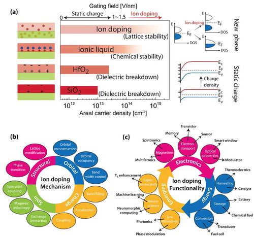
Ion doping typically initiates at material interfaces, which are classified as (a) the solid-gas interface, (b) the solid-liquid interface, and (c) the solid-solid interface, as shown in )–(c). Researchers have investigated H+ doping through solid-gas interfaces for strongly correlated oxides SmNiO3 [Citation17] and VO2 [Citation8,Citation9]. In a redox environment, VO2 can be H+ doped with variable concentration by adjusting the annealing temperature [Citation39]. Metallization of VO2 has been observed after annealing at relatively modest temperatures (50–200°C) following the early work of Andreev et al. [Citation9,Citation40,Citation41] Others have found that light irradiation can be a powerful means of assisting ion doping processes such that it can take place at room temperature [Citation13,Citation42]. Another effective H+ doping technique is the catalytic spillover method with Pt electrodes, which has been explored for SmNiO3 [Citation17]. At the triple phase boundary of Pt-SmNiO3-H2, H2, molecules dissociate into atomic hydrogen and split into H+ and e−, which are then incorporated into the SmNiO3 lattice. This process realizes electron doping, and electronic transport is suppressed via electron-electron correlations [Citation17]. Hydrogenation, however, interestingly, insulating behavior of highly doped VO2 has been observed after hydrogen doping catalyzed by Pt nanoparticles [Citation8]. This doping process is reversible, and hydrogen can escape from a material by heating in air.
Figure 4. The mechanisms to introduce ions into the materials though (a) Solid-Gas, (b) Solid-Liquid, and (c) Solid-Solid interfaces.
Ion doping across solid-liquid interfaces can also be realized by using aqueous solutions, ionic liquids, or water. For example, dipping VO2 into a H+-containing aqueous solution such as glycerol results in metallization of the oxide [Citation41]. In ionic liquid gating, owing to a very strong electric field (≥10 MV/cm) at the interface, oxygen can be drawn out from a material and into the ionic liquid, or hydrogen ions can be intercalated into the material from the ionic liquid, depending on the polarity of the electric field. As a result, large change in resistance or optical transmittance can take place in several materials. Up to now, ionic liquid gating experiments have been conducted for many systems including VO2 [Citation10,Citation37], SmNiO3 [Citation17,Citation43], (Fe, Zn)3O4 [Citation36,Citation44], etc. (see more details in Section 3). Water has also been used as a gating medium for H+ doping. When a voltage of over 1.23 V is applied between an electrode and a material in water, it ionizes to form H+ and OH−. Thus, under the application of a positive electric field, H+ can be intercalated into the material [Citation45]. For SrTiO3-based FETs [Citation46] and side-gated FETs based on VO2 [Citation47], it was demonstrated that a water-infiltrated nanoporous glass or a humid air gap can be employed for modulating the channel conductance, respectively.
Ion doping across solid–solid interfaces has been demonstrated using solid-state electrolytes. When a positive bias is applied across a proton-storing solid-state electrolyte, hydrogen ions can be injected into a material. The advantage of this doping method is that not only H+ but also Li+ and Mg2+ intercalation can take place in a controlled manner by gating through electrochemical cells [Citation17]. Electric-field-induced hydrogen injection is non-volatile and reversible. After removal of an applied electric field, ionic dopants remain in the material, and the application of a reverse electric-field can be used to remove them. Therefore, these phenomena can be exploited for use in non-volatile memory devices with cross-bar or related geometries.
2.2 X-ray-based characterization and in situ studies
The introduction of ions into a material generally induces structural, chemical and electronic modifications, albeit weak or subtle in many cases. These changes can be reliably and precisely detected by modern X-ray techniques in distinct ways [Citation48]. In this section, we discuss and illustrate a few representative X-ray scattering, spectroscopic, and imaging techniques useful for ex situ/in situ characterization and probing both macro- and microscopic changes in an evolving material owing to the formation, migration, and re-distribution of ionic species. In the hard X-ray regime (> 4 keV), X-rays can penetrate into complex environments (whether gas, liquid, or solid media), allowing studies of sub-Ångstrom-level changes to a material in-situ/operando without severe beam effects. The structural sensitivity from X-ray scattering can be complemented with chemical specificity, either by energy-dependent scattering (e.g. resonant/inelastic scattering) or with spectroscopic techniques, capturing the energy spectrum of the emitted photons or electrons. In the soft X-ray regime (<4 keV), despite limited penetration and spatial resolution, versatile spectroscopic techniques dedicated to light elements (e.g. C, N, and O) and transition metal families (e.g. 3d/4d) can provide exclusive information on the atomic composition, local bonding and coordination, as well as electronic configurations (e.g. band structure, orbital filling, and spin orientation). The combination of X-ray characterization in both hard and soft regimes has become key to developing a fundamental understanding of functional materials and devices that exploit controlled ionic behaviors. Moreover, many synchrotron facilities now allow substantial X-ray focusing such that changes within microscopic regions can be thoroughly investigated in detail with X-ray imaging and microscopy multi-modalities [Citation49]. The ever-improving degree of X-ray coherence due to upgrades in synchrotron sources makes it easier to directly catch and view ionically affected regions in real space with temporal correlations. The newest generation of synchrotrons is developing X-ray toolkits for such purposes [Citation50].
The chemical valence state and electronic band structure changes due to the insertion or removal of ionic species of materials can be effectively detected by X-ray spectroscopy measurements including photoelectron- and fluorescence-based collection modes. In the exploration of a hydrogen-doping-induced, multistep phase transformation of strongly correlated VO2 thin films, Yoon et al. show that the relatively open rutile framework of VO2 allows reversible hydrogen doping [Citation8]. Catalytically active Pt nanoparticles assist the doping of hydrogen into the pristine, insulating VO2 to form metallic HxVO2 phase in the first step; further hydrogenation leads to the creation of another insulating phase, HVO2. The systematic change in the vanadium oxidation state was confirmed by X-ray photoelectron spectroscopy (XPS), as shown in (a). The HVO2 film is comprised primarily of V3+ as compared to the pristine VO2 film exhibiting mainly V4+. Moreover, the HVO2 sample shows a significant increase of intensity from O-H bonds. Near-edge X-ray absorption fine structure (NEXAFS) measurements at both the vanadium L-edge and oxygen K-edge ( (b–c)) probe the effect of hydrogenation on filling of the t2g portion of the conduction band. Other than the expected shifts in the V LIII and V LII edges (), there is a large decrease in the intensity of the t2g-related p band at the O K-edge (), which is likely due to electron transfer from hydrogen to vanadium, leading to the insulating behavior [Citation8].
Figure 5. X-ray photoemission and absorption spectroscopy revealing hydrogenation-induced electronic phase transition in VO2 thin film [Citation8]. (a) V 2p and O 1s core-level spectra of pristine VO2 and fully hydrogenated insulating HVO2, confirming the V valence change and the existence of O–H bonding after hydrogenation. (b) and (c) show the V L-edge and O K-edge NEXAFS of pristine VO2 and fully hydrogenated insulating HVO2. The chemical shift of the V L-edge and the suppression of the t2g band peak in O K-edge are clearly observed in fully hydrogenated HVO2 films. Reproduced with permission from Ref. [8] © Springer Nature 2016.
![Figure 5. X-ray photoemission and absorption spectroscopy revealing hydrogenation-induced electronic phase transition in VO2 thin film [Citation8]. (a) V 2p and O 1s core-level
spectra of pristine VO2 and fully hydrogenated insulating HVO2, confirming the V valence change and the existence of O–H bonding after hydrogenation. (b) and (c) show the V L-edge and O K-edge NEXAFS of pristine VO2 and fully hydrogenated insulating HVO2. The chemical shift of the V L-edge and the suppression of the t2g band peak in O K-edge are clearly observed in fully hydrogenated HVO2 films. Reproduced with permission from Ref. [8] © Springer Nature 2016.](/cms/asset/68b741af-1565-49db-a605-36ffdb47651f/tapx_a_1523686_f0005_oc.jpg)
With regard to detecting changes to the ion concentration profile inside a material, the resulting effect on average lattice structure can be sensitively probed by X-ray diffraction through changes to the position of Bragg peaks [Citation3,Citation51–Citation53]. A recent study of a strongly correlated fuel cell electrolyte [Citation5] demonstrates that proton incorporation into SmNiO3 lattice engenders substantial changes to its electronic and ionic conductivity. The chemical reduction of Ni3+ to Ni2+ could be resolved not only spectroscopically but also structurally, due to the larger ionic radius of Ni2+ and an elongation of the Ni-O bond coupled with electron localization, as shown in ). The electronic change in the hydrogenated regions evident by greater optical transparency is illustrated in ). ) exhibits a series of specular diffraction scans for a SmNiO3 epitaxial film grown on LaAlO3 around the (002) reflection. The pristine and hydrogenated sections of the SmNiO3 film have characteristic Bragg reflections at different qz positions (where the scans were measured at spots A, B, C, and D, shown in ). Real space maps collected at the different qz are shown in -f) revealed that the regions between the catalytic Pt electrodes show the greatest amount of proton incorporation, i.e. the contrast in ) is reversed when compared to ). Hence, it is important to know where to investigate in reciprocal space a priori and exploit in situ/operando techniques to monitor whether the observed changes are indeed caused by the formation and migration of ionic species [Citation49].
Figure 6. Synchrotron structural characterization of the emergent strongly correlated SmNiO3 (SNO) phase [Citation5]. (a) A larger crystal radius of Ni2+ and electron localization can induce an increase in the lattice spacing. (b) An optical image of a hydrogenated SNO sample. (c) X-ray diffraction patterns from the various spots A, B, C and D marked in (b). The difference in the lattice spacing change can be related to the decreasing doping concentration with increasing diffusion length from the triple phase boundary where hydrogen enters SmNiO3. (d) Real-space mapping of the intensity of the Pt (111) peak at qz = 2.78 Å−1 (e) the H-SNO peak 1 at qz = 3.18 Å−1 (e) and the H-SNO peak 2 at qz = 2.98 Å−1 (f) A clear positive correlation between the Pt (111) and the qz = 2.98 Å−1 peaks can be seen, whereas the Pt (111) and qz = 3.18 Å−1 peaks show a negative correlation. Reproduced with permission from Ref. [5] © Springer Nature 2016.
![Figure 6. Synchrotron structural characterization of the emergent strongly correlated SmNiO3 (SNO) phase [Citation5]. (a) A larger crystal radius of Ni2+ and electron localization can induce an increase in the lattice spacing. (b) An optical image of a hydrogenated SNO sample. (c) X-ray diffraction patterns from the various spots A, B, C and D marked in (b). The difference in the lattice spacing change can be related to the decreasing doping concentration with increasing diffusion length from the triple phase boundary where hydrogen enters SmNiO3. (d) Real-space mapping of the intensity of the Pt (111) peak at qz = 2.78 Å−1 (e) the H-SNO peak 1 at qz = 3.18 Å−1 (e) and the H-SNO peak 2 at qz = 2.98 Å−1 (f) A clear positive correlation between the Pt (111) and the qz = 2.98 Å−1 peaks can be seen, whereas the Pt (111) and qz = 3.18 Å−1 peaks show a negative correlation. Reproduced with permission from Ref. [5] © Springer Nature 2016.](/cms/asset/9c49bf02-ab54-4483-bf35-36ea40c216cc/tapx_a_1523686_f0006_oc.jpg)
Note that the effectiveness of the lattice structure detection depends on the chemical expansivity of the oxide [Citation54,Citation55]. In some cases, the lattice changes can be very subtle and inhomogenous along the thickness direction [Citation56]. In this case, surface X-ray diffraction (SXRD) and measurement of the crystal truncation rods (CTRs) is a valuable technique for the investigation of such small changes in epitaxial thin films, as the incidence angle of the X-rays with respect to the sample is kept low to maximize signal from the thin film. The resulting scattering takes the form of an interference pattern comprising Bragg rods from both the epitaxial layer and the substrate [Citation57]. Since the scattering is kinematical, the intensities along the Bragg rods can be fully analyzed in a straightforward manner with model-dependent fitting or taking advantage of phase-retrieval algorithms for reconstructing the complete atomic structures [Citation58]. These methods have proven useful for imaging the depth-resolved atomic structure and rendering a layer-by-layer density profile along the out-of-plane direction [Citation59]. Spatial variations across the lateral dimensions of an epitaxial film are ‘folded’ together in SXRD, in effect averaging the structure along these dimensions [Citation60].
If probing lateral inhomogeneities of ionic profile or motion is desired, one can employ scanning micro- or nanoprobe beams to measure and determine the variations in chemical profile and atomic structure along the lateral directions [Citation49]. The ability to gain quantitative understanding of the complex interactions between the electric field and ionic defects in a memristive device, as well as the dynamic flow of defects, is necessary for the development of high-endurance devices such as memristors [Citation61]. The microscopic picture underlying a memristive device is made complex by the many possible chemical reactions and defect generation/redistribution triggered by the electric field, thermal gradients, and chemical concentration gradients [Citation62]. Therefore, multimodal imaging with structural and chemical information in a working device is necessary for clarifying the detailed microscopic mechanisms. In a recent study of electrically cycled TaOx memristor devices by Kumar et al., operando X-ray absorption spectromicroscopy is utilized as a powerful element-specific local probe for investigating chemical and electronic variations of the functional oxide channel, in particular catching inhomogeneous localized phenomena related to device evolution and failure with electrical cycling [Citation61]. ), shows an apparatus at the Advanced Light Source spectromicroscopy beamline for focusing the incoming beam and scanning the sample along the lateral directions of a crossbar TaOx memristor device, while maintain specific X-ray energies. Both O K-edge and Ta L3-edge absorption spectroscopy were used to spatially map the unoccupied partial density of states of the TaOx film at different resistive switching states. Upon high voltage electrical cycling of the TaOx devices, the irreversible development of insulating, submicron features with a ring of oxygen interstitials and an inner core of oxygen vacancies was imaged with spectromicroscopy, as exhibited in –e). The radial oxygen migration can be well reproduced by a thermophoresis microscopic model involving thermally-driven lateral forces during dynamic evolution of the conduction channel. Moreover, the same team developed the capability of time-multiplexed spectromicroscopy to resolve weak-signal variations and subtle, localized modifications in a memristor with spatial and energy resolutions of ~30 nm and 70 meV [Citation63]. These spectromicroscopy observations have helped to verify different theoretical models regarding oxygen ion migration, ionic defect clustering, localized thermal dissipation, and possible failure mechanisms of resistance switching [Citation62].
Figure 7. Operando X-ray spectromicroscopy capturing the active region of a working memristive device [Citation61]. (a) Schematic of X-ray spectromicroscopy experimental setup including the X-rays and the cross-point device. (b) O K-edge X-ray transmission intensity images of a cross-point device after different numbers of applied 5 V cycles. All maps were obtained using single X-ray energies between 530 and 533 eV. Blue arrows point to particular ring-like features in the maps. (c) O K-edge transmission intensity map of a different device cycled to 120,000 cycles imaged at an energy of 531.2 eV. (d) 3D color-intensity plot of the ring seen in c displaying the profile of the ring of oxygen species. (e) Upper panel: O K-edge absorption spectra collected in the bright and dark regions of the device. The decomposition of the spectra into sub-bands was accomplished by fitting separate peaks. Vertical dotted lines indicate the position of the lowest conduction band, with corresponding colors. Lower panel: Difference between O K-edge spectra with and without current obtained synchronously in the same spatial regions as the spectra shown in the upper panel. Reproduced with permission from Ref. [61] © John Wiley and Sons 2016.
![Figure 7. Operando X-ray spectromicroscopy capturing the active region of a working memristive device [Citation61]. (a) Schematic of X-ray spectromicroscopy experimental setup including the X-rays and the cross-point device. (b) O K-edge X-ray transmission intensity images of a cross-point device after different numbers of applied 5 V cycles. All maps were obtained using single X-ray energies between 530 and 533 eV. Blue arrows point to particular ring-like features in the maps. (c) O K-edge transmission intensity map of a different device cycled to 120,000 cycles imaged at an energy of 531.2 eV. (d) 3D color-intensity plot of the ring seen in c displaying the profile of the ring of oxygen species. (e) Upper panel: O K-edge absorption spectra collected in the bright and dark regions of the device. The decomposition of the spectra into sub-bands was accomplished by fitting separate peaks. Vertical dotted lines indicate the position of the lowest conduction band, with corresponding colors. Lower panel: Difference between O K-edge spectra with and without current obtained synchronously in the same spatial regions as the spectra shown in the upper panel. Reproduced with permission from Ref. [61] © John Wiley and Sons 2016.](/cms/asset/18e70b99-81bb-4ded-9d76-1879e2f906c9/tapx_a_1523686_f0007_oc.jpg)
Unlike scanning X-ray probe techniques [Citation64], X-ray reflection interface microscope (XRIM) is a full-field, hard X-ray microscope and a multiscale probe for conducting in situ studies of the time evolution of lateral features as a result of ionic defect formation and migration in thin film materials. XRIM uses the surface scattering signal in a reflection geometry to spatially resolve various local surface/interfacial structures (e.g. defect clusters, dislocation networks, structural domains, and surface/interface topography) with 50 nm lateral spatial resolution (depending on the resolution of the objective lens) and atomic height sensitivity [Citation65,Citation66]. The major advantage of XRIM lies in the full-field nature of the technique (e.g. allowing a 20 × 20 μm [Citation2] field of view) as well as sub-second time resolution [Citation67,Citation68], which stands in sharp contrast with the more time-consuming scanning X-ray probes. Furthermore, the XRIM technique can be extended and implemented with resonant X-ray mode for chemical sensitivity.
The fast developing and emerging coherent X-ray techniques will bring additional imaging capabilities [Citation50,Citation69,Citation70] for the study of ion-doped materials and related devices. Instead of using a lens to form the sample image, coherent diffraction imaging (CDI) relies on capturing the interference pattern produced by coherent diffraction and exploiting phase-retrieval algorithms to reconstruct the three-dimensional electron density and atomic displacement fields in materials [Citation71,Citation72]. The remarkable sensitivity of CDI in the Bragg geometry (BCDI) to the internal structure of a sample has made it a powerful tool for imaging local, nanoscale lattice distortions [Citation73]. The displacement field determined with BCDI is crucial for identifying the character of different structural imperfections; BCDI can thus be used to track buried single defects with nanoscale resolution [Citation74,Citation75]. As illustrated in ), three-dimensional imaging of topological defect dynamics in individual lithium battery cathode nanoparticles has been recently accomplished by employing BCDI under operando conditions [Citation76]. It was shown by Ulvestad et al. that the lithium-rich phase nucleates near the dislocation and spreads in-homogeneously during the structural phase transformation. Using the dislocation field as a local probe of elastic properties, they also revealed that a negative Poisson’s ratio can emerge at a region of the electrode material under high electrochemical potentials. Although operando BCDI on defect structures has been limited to imaging dislocations in crystals, there have been continuing developments in analysis [Citation77,Citation78] and experimental practice [Citation79] for different categories of lattice defects, including ionic defects (e.g. cation/anion vacancies). Other than imaging lattice distortions, coherent techniques like X-ray photon correlation spectroscopy (XPCS) enable access to information regarding lattice dynamics (i.e. equilibrium or non-equilibrium structural fluctuations) by constructing the autocorrelation function in the time domain from each coherently scattered phase object (speckles) [Citation80]. XPCS can be applied to the surfaces or buried interfaces of thin film materials in complex environments to monitor their temporal evolution [Citation81,Citation82]. As demonstrated in ), Bragg-geometry XPCS has been employed to study the thermal fluctuations of ferroelectric nanodomains in oxide superlattices, which exhibit a continuous temporal decorrelation due to spontaneous domain fluctuations (e.g. spatial disorder) [Citation83]. Extended XPCS measurements to probe heterogeneous domain dynamics of ionic defects (i.e. ordered or correlated oxygen vacancies) in functional materials can be envisioned. The tremendous enhancement in X-ray brightness and coherence to be delivered in nearly diffraction-limited synchrotron sources (e.g. as from an upgraded Advanced Photon Source) will enable a new frontier of X-ray characterization and greatly improved understanding of ion doped materials.
Figure 8. Bragg coherent diffractive imaging and X-ray photo correlation spectroscopy imaging defects [Citation76] and probing disorders [Citation83]. Coherent X-rays are incident on a lithium ion battery cathode nanoparticle (green) containing an edge dislocation. (a) Schematic of an edge dislocation for a cubic unit cell structure is shown with the extra half plane colored purple. The diffracted X-rays carry information about the 3D electron density and atomic displacement fields within the particle that allows the type of dislocation to be identified and visualized. (b) Upper left: Coherent X-rays are incident on a PbTiO3/SrTiO3 ferroelectric superlattice which has serpentine stripe domain patterns with up and down polarization down to the perovskite unit cell level. Upper right: In the reciprocal space scattering geometry, the Ewald sphere intersects the ring of domain diffuse scattering (green ring), but does not pass through the (002) superlattice Bragg reflection (red sphere). Lower: Two-time correlation map for coherent domain diffuse scattering patterns near phase transition temperature. Reproduced with permissions from Ref. [76] © The American Association for the Advancement of Science 2015, Ref. [83] © The American Physical Society 2017.
![Figure 8. Bragg coherent diffractive imaging and X-ray photo correlation spectroscopy imaging defects [Citation76] and probing disorders [Citation83]. Coherent X-rays are incident on a lithium ion battery cathode nanoparticle (green) containing an edge dislocation. (a) Schematic of an edge dislocation for a cubic unit cell structure is shown with the extra half plane colored purple. The diffracted X-rays carry information about the 3D electron density and atomic displacement fields within the particle that allows the type of dislocation to be identified and visualized. (b) Upper left: Coherent X-rays are incident on a PbTiO3/SrTiO3 ferroelectric superlattice which has serpentine stripe domain patterns with up and down polarization down to the perovskite unit cell level. Upper right: In the reciprocal space scattering geometry, the Ewald sphere intersects the ring of domain diffuse scattering (green ring), but does not pass through the (002) superlattice Bragg reflection (red sphere). Lower: Two-time correlation map for coherent domain diffuse scattering patterns near phase transition temperature. Reproduced with permissions from Ref. [76] © The American Association for the Advancement of Science 2015, Ref. [83] © The American Physical Society 2017.](/cms/asset/49ef39a6-76ba-4552-ab15-7673bda41943/tapx_a_1523686_f0008_oc.jpg)
2.3 Real-space probe characterization and in-situ studies
Real-space probes allow the direct visualization of ion-electron coupled motion inside materials or across physical boundaries with atomic resolution. By monitoring ionic activity due to local chemical and electronic structural perturbations with site-specific sensitivity, they can facilitate the design of novel, ionically driven materials systems and devices in a variety of energy and electronic technologies [Citation84]. In this section, we highlight two imaging modalities at the frontier of quantitative ex-situ/in-situ atomic visualization and probing site-dependent ionic activities in materials.
The resolution of modern, aberration-corrected (scanning) transmission electron microscopes (STEM) allows imaging of the oxygen sub-lattices, providing details on octahedral distortions, tilts/rotations, and site occupancy via the angular bright-field or negative Cs imaging technique [Citation85–Citation87]. Recent progresses have demonstrated how such methods provide insight into defect distribution and evolution. For instance, in an in situ study of electrically induced oxygen migration and subsequent phase transformation in a SrCoO2.5−σ epitaxial thin film [Citation88], state-of-the-art STEM characterization revealed the extraction pathway of oxygen ions from every other SrO layer under an electrical bias as well as the abrupt structural collapse beyond the critical bias voltage of 1.5 V. The in situ visualization of the low-Z oxygen columns suggested that the highly ordered oxygen vacancy rows are not only intrinsic ionic diffusion highways but also energetically favorable sites for the formation of vacancies. The results elucidate the atomistic mechanisms of field-induced topotactic phase transformations via electro-chemo-mechanical coupling [Citation88]. In another case study, in situ STEM was used to observe oxygen vacancy formation in LaCoO3 epitaxial heterostructures in real-time under electron beam irradiation [Citation89], as shown in ). The dynamics of the nucleation, growth, and defect entanglements strongly couple to the resulting electronic and magnetic properties, making these STEM observations of the phase transition essential. In addition, these in situ imaging techniques have been extended to more complex environments, such as ionic liquid gating where highly anisotropic phase transformations between the brownmillerite SrCoO2.5 and the perovskite SrCoO3 thin film (e.g. the phase boundary propagating much faster laterally than through the thickness of the film) can occur deep below the gated surface ()) [Citation90].
Figure 9. Advanced real-space characterization and in situ studies of ionotronic materials and devices. (a) In situ STEM observation of oxygen vacancy dynamics and ordering in the epitaxial LaCoO3 thin film induced by the electron beam irradiation [Citation89]. (b) In situ TEM measurements investigating ionic liquid gating effect for SrCoOx thin film with ionic liquid placement by an atomic force microscope tip [Citation90]. Gate voltages with both polarities are applied to the ionic liquid via the gate electrode. STEM-HAADF images of the pristine SrCoO2.5 film and the altered film after gating with – 3V bias are shown. The white scale bar corresponds to 2 nm. (c) The schematic principle of electrochemical strain microscopy (ESM) [Citation95]. In ESM, the ionic motion and the resulting surface strain induced by the applied bias through the contact tip is detected by the SPM rendering a map of the ionic activity at the nanoscale. (d) Spatially resolved imaging of ionic conduction channels in the nanocomposite film comprised of SrTiO3 and Sm-doped CeO2 nanopillars (STO-SDC) [Citation96]. The image sizes are all 250 × 125 nm2. Spatial maps of current response and relative FORC-IV loop area captured at the tip bias voltage of −8 V. Current versus tip bias voltage plots were collected respectively at the SDC nanopillars core and the STO region, illustrating the significant difference in local ionic activities. Reproduced with permission from Ref. [89] © Wiley 2017, Ref. [90] © Creative Commons Attribution 4.0 International License, Ref. [95] © Wiley 2010, Ref. [96] © Creative Commons Attribution 4.0 International License.
![Figure 9. Advanced real-space characterization and in situ studies of ionotronic materials and devices. (a) In situ STEM observation of oxygen vacancy dynamics and ordering in the epitaxial LaCoO3 thin film induced by the electron beam irradiation [Citation89]. (b) In situ TEM measurements investigating ionic liquid gating effect for SrCoOx thin film with ionic liquid placement by an atomic force microscope tip [Citation90]. Gate voltages with both polarities are applied to the ionic liquid via the gate electrode. STEM-HAADF images of the pristine SrCoO2.5 film and the altered film after gating with – 3V bias are shown. The white scale bar corresponds to 2 nm. (c) The schematic principle of electrochemical strain microscopy (ESM) [Citation95]. In ESM, the ionic motion and the resulting surface strain induced by the applied bias through the contact tip is detected by the SPM rendering a map of the ionic activity at the nanoscale. (d) Spatially resolved imaging of ionic conduction channels in the nanocomposite film comprised of SrTiO3 and Sm-doped CeO2 nanopillars (STO-SDC) [Citation96]. The image sizes are all 250 × 125 nm2. Spatial maps of current response and relative FORC-IV loop area captured at the tip bias voltage of −8 V. Current versus tip bias voltage plots were collected respectively at the SDC nanopillars core and the STO region, illustrating the significant difference in local ionic activities. Reproduced with permission from Ref. [89] © Wiley 2017, Ref. [90] © Creative Commons Attribution 4.0 International License, Ref. [95] © Wiley 2010, Ref. [96] © Creative Commons Attribution 4.0 International License.](/cms/asset/94ddb1e8-2fce-444b-a84e-7e16d19efe9a/tapx_a_1523686_f0009_oc.jpg)
There have also been a number of important developments in scanning probe microscopy (SPM) over the last decade that permit quantitative understanding of the local atomic and electronic structures of surfaces as well as nanoscale chemical and mechanical responses of functional interfaces under various external stimuli [Citation91,Citation92]. For example, Sharma et al. utilized Kelvin probe force microscopy (KPFM) and conducting atomic force microscopy (CAFM) to study the metal insulator transition (MIT) in epitaxial VO2 thin films with SPM-tip induced electrochemistry [Citation93]. By alternating between positive and negative biases, the tip-scanned areas of the VO2 film exhibited significant electric field-modulated MIT behavior at the nanoscale via changes in the contact potential difference and strain-induced surface oxygen off-stoichiometry. This highlights the critical role of oxygen vacancies in controlling the MIT and their utility for developing novel electronic and ionotronic devices. Electrochemical strain microscopy (ESM) (schematically shown in )) [Citation94], used to probe local ionically-driven behaviors, is based on the tip sensitivity to ionic mass flow near the surface region, and in particular the local strains induced by changes in the concentration of ionic species (Vegard strain) [Citation92,Citation95]. The detected strain from ESM can be directly linked to the number of transferred ions, thus providing information scalable with that obtained by macroscopic electrochemical characterization methods [Citation84]. Yang et al. recently used SPM-ESM to explore oxygen ion transport in the heteroepitaxial nanocomposite comprising SrTiO3 and Sm-doped CeO2 nanopillars (STO-SDC) [Citation96]. As shown in ), they found that the ionic conductivity is at least one order of magnitude larger than homogeneous SDC thin films. From in-situ nanoscale mapping of the electrochemical oxidation- reduction process at different temperatures, Yang et al. found that the fast ionic-conduction channels were not exclusively limited to the nanocomposite interface regions but rather distributed within the volume of the crystalline SDC nanopillars. Such direct visualization of spatially confined fast ionic/electronic transport by site-specific ESM imaging promotes improved understanding of the mechanism of ion conductivity enhancement in oxide heterostructures [Citation97], superlattices, and nanocomposites [Citation98] designed for low-temperature operation of ionotronic devices.
3 Control of physical properties
3.1 Modification of electrical, optical and magnetic properties
The electrical properties of materials such as transition metal oxides, are quite sensitive to the valence state of the transition metals [Citation99,Citation100], which can be easily changed by chemical doping [Citation101,Citation102]. Along with changes in electrical properties, the modified carrier concentration or band structure can vary the optical properties of materials by changing their absorption or reflection characteristics. Moreover, reversible ion doping, assisted by electric fields can reduce or oxidize certain magnetic ions and thus control their magnetic properties [Citation7,Citation103,Citation104].
3.1.1 Electric field assisted ion migration
As shown in ), under electric field, protons migrate in the crystal lattice, leading to spatial modulation of the physical properties. Resistive switching-based non-volatile memory devices (also called ReRAM) have recently emerged, utilizing redox reactions for their operation (typically oxygen diffusion through a oxide) [Citation105]. The switching mechanism of ReRAM is based on the formation/dissolution of local metallic/oxygen-deficient filaments, while the global composition is unchanged. Alternatively, the operation of non-volatile electric double layer (EDL) devices depends on the modulation of entire interface or bulk composition due to ionic migration. From this point of view, iontronic devices are quite different from filamentary ReRAM.
Figure 10. (a) Schematic illustrations of the concept of electric field assisted ion (proton) migration device. (b) Out of plane ion migration geometry at interface. (c) In-plane ion migration geometry at interface.
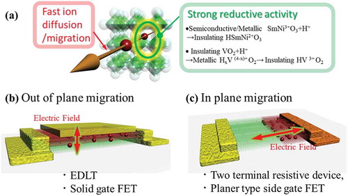
Electric-field-assisted ion migration devices can be fabricated with two-different geometries. ,c) show devices with ions migrating out of plane and in-plane with respect to the interface. The out-of-plane ion migration can be implemented using a three-terminal, electrochemical field effect transistor. Application of an electric field shuttles protons in and out of the solid-liquid interface (electric double layer and water-infiltrated gating) or the solid-solid interface (solid state electrolyte gating), quickly changing the conductance of the channel layer. In EDL-transistor (EDLT) gating, the capacitance of the gating medium and the channel thickness are both important factors for enhancing the magnitude of the resistance modulation. Indeed, it is known that ionic liquids with smaller molecules have larger capacitances, thus permitting larger on-off ratios [Citation106], ), shows a (Fe, Zn)3O4 EDLT device with a well-defined channel oxide layer, which shows a higher on-off ratio when the channel becomes thinner (the change of nonvolatile channel conductance, , are 2.5% for 11 nm channel thickness and 7.8% for 7 nm, respectively) [Citation107]. This indicates that the chemical reduction occurs not in the bulk of the channel but at the solid-liquid interface and vicinity on the channel near the interface as shown in ). The channel resistance can be well explained by a two resistor model of
, where ΔG, tr, tf, σr, σf are the change of nonvolatile channel conductance at zero bias, the thickness of the ion migrated layer at the interface, the channel thickness, the conductivity of the interface layer, and the conductivity of the pristine channel layer, respectively. In (Fe, Zn)3O4 EDLT devices, the thickness of the interface ion migrated layer is estimated to be 0.63 nm [Citation107]. For device applications, solid-state gating is often preferred, and Shi et al. demonstrated a colossal change in the conductivity of the SmNiO3 channel in a solid-state protonic transistor. The gating medium consisted of the combination of a low-temperature proton conductor (yttrium-doped barium zirconate) as a proton reservoir and a hydrogen molecule dissociation layer of Pd, as shown in ].
Figure 11. (a) EDLT devices composed of (Fe,Zn)3O4 channel and TEM image for their interface [Citation44]. (b) Schematic cross-sectional image of the conduction channel. (c) Layout of the solid-state proton SmNiO3 transistor, where SmNiO3 serves as the channel layer, yttrium-doped barium zirconate (BYZ) as proton reservoir, (yttria-stabilized zirconia) YSZ as gate insulator, Pd as gate electrode as well as H2 dissociation catalyst [Citation17]. Reproduced with permissions from Ref. [44] © John Wiley and Sons 2014, Ref. [17] © Springer Nature 2014.
![Figure 11. (a) EDLT devices composed of (Fe,Zn)3O4 channel and TEM image for their interface [Citation44]. (b) Schematic cross-sectional image of the conduction channel. (c) Layout of the solid-state proton SmNiO3 transistor, where SmNiO3 serves as the channel layer, yttrium-doped barium zirconate (BYZ) as proton reservoir, (yttria-stabilized zirconia) YSZ as gate insulator, Pd as gate electrode as well as H2 dissociation catalyst [Citation17]. Reproduced with permissions from Ref. [44] © John Wiley and Sons 2014, Ref. [17] © Springer Nature 2014.](/cms/asset/ea491c44-ed10-4a48-b3b3-9e6ec1c1dc4c/tapx_a_1523686_f0011_oc.jpg)
An in-plane ion-migration device is illustrated in ). The application of an electric field between two electrodes leads to the migration of protons and consequently the modulation of the spatial proton distribution. Such proton-based in-plane resistive switching memory has been demonstrated using strongly correlated oxides of NdNiO3 [Citation31] and VO2 [Citation47], ), shows a SmNiO3 film defined with asymmetric contacting electrodes of Pt and Au. Using the Pt catalytic spillover method via the solid-gas interface, protons can be injected into the SmNiO3 film only near the Pt electrode. The application of a positive bias at the Pt electrode leads to the enlargement of the hydrogenated area (which is the high resistive state) due to the migration of protons into the entire film, while the negative bias application results in the reduction of the hydrogenated area. With this property, proton-based resistive memory devices can be fabricated. Oh et al. reported similar proton-based resistive switching memory devices in NdNiO3 with asymmetrical concentration of protons, as shown in ] High speed multi-state memory devices have been recently demonstrated utilizing proton re-distribution in nickelates under pulsed voltages moving this concept closer to GHz electronics [Citation108]. Another example is a planar VO2 FET device with a humid-air gap as the gating medium ()) [Citation47]. In this device, the electric field is converged at the edges of the VO2 channel, which is covered by adsorbed H2O. Thus, by applying a gate bias voltage (VG), water-mediated H+ incorporation occurs at the channel edges, followed by H+ diffusion into the VO2 channel, leading to the metallization. ) shows spatial mapping of the hydrogen element ratio in the device after applying the gate bias, which was investigated by time-of-flight secondary ion mass spectrometry (Tof-SIMS). The hydrogen content in the VO2 channel is higher than that in other areas of the device after applying VG. These results provide direct evidence of H+ intercalation into the VO2 channel. Besides the FET devices, the resistance of SmNiO3 is highly sensitive to the applied electrical bias in salt water [Citation4]. As shown in ), due to the water-mediated H+ incorporation, the resistivity of SmNiO3 increases after a negative bias is applied. This proton doping in SmNiO3 potentially enables detection of the electric signals spanning from naval vessels down to the bioelectric potentials emitted by numerous marine species.
Figure 12. (a) Optical microscope image of SmNiO3 with asymmetric electrodes (Pt and Au). (b) Two-terminal current-voltage characteristics of ‘asymmetrical’ H-Pt/NNO/NH-Pt (black line), ‘symmetrical’ NH-Pt/NNO/NH-Pt (red line) and H-Pt/NNO/H-Pt (blue line). The inset shows schematic illustration of NdNiO3 with asymmetric electrodes [Citation31]. (c) An atomic force microscopic (AFM) image of VO2 nanowire device with air gap planar-type gates [Citation47]. (d) The relative elemental ratios of hydrogen normalized by oxygen in a device after applying VG = 100 V and in a pristine device. The solid and dashed green lines represent the averages of the hydrogen atom profiles and the standard deviations [Citation47]. (e) The resistance change of SmNiO3 due to the water-mediated hydrogenation as a function of applied bias [Citation4]. The nickelate sensor may detect the electric signal spanning from small marine animals to naval vessels, the magnitude of electric signals of which are indicated by black arrows respectively. Reproduced with permissions from Ref. [31] © AIP Publishing 2016, Ref. [47] © Springer Nature 2015, Ref. [4] © Springer Nature 2017.
![Figure 12. (a) Optical microscope image of SmNiO3 with asymmetric electrodes (Pt and Au). (b) Two-terminal current-voltage characteristics of ‘asymmetrical’ H-Pt/NNO/NH-Pt (black line), ‘symmetrical’ NH-Pt/NNO/NH-Pt (red line) and H-Pt/NNO/H-Pt (blue line). The inset shows schematic illustration of NdNiO3 with asymmetric electrodes [Citation31]. (c) An atomic force microscopic (AFM) image of VO2 nanowire device with air gap planar-type gates [Citation47]. (d) The relative elemental ratios of hydrogen normalized by oxygen in a device after applying VG = 100 V and in a pristine device. The solid and dashed green lines represent the averages of the hydrogen atom profiles and the standard deviations [Citation47]. (e) The resistance change of SmNiO3 due to the water-mediated hydrogenation as a function of applied bias [Citation4]. The nickelate sensor may detect the electric signal spanning from small marine animals to naval vessels, the magnitude of electric signals of which are indicated by black arrows respectively. Reproduced with permissions from Ref. [31] © AIP Publishing 2016, Ref. [47] © Springer Nature 2015, Ref. [4] © Springer Nature 2017.](/cms/asset/f2ca7b9f-7538-41e1-b47a-3206e4a1381f/tapx_a_1523686_f0012_oc.jpg)
In electric field-assisted ion (proton) migration devices, the ionic fluxes depend on the ion concentration gradient as well as the electric-field [Citation109]. Thus, the H+ flux (JH) can be described as where nH is the H+ concentration in the channel, D is the diffusion coefficient, and μ is the mobility of ions under the electric field E. For enhancing the modulation efficiency, it was reported that narrowing the channel width is important for planar VO2-FETs [Citation45], so that the ion diffusion length is one of the key properties. In addition, the mass and diameter of the hydrogen ion are only 6% and 25% in comparison to the oxygen ion, making D and μ larger for hydrogen ions.
3.1.2 Control of optical and magnetic properties
The modified electronic band structure via ion doping can result in large changes in the optical properties of materials. The changes are typically due to either opening of the band gap or variations in the optical constants at certain wavelengths. Normally, protons [Citation3,Citation110,Citation111], oxygen vacancies [Citation112,Citation113], small ions [Citation114,Citation115], and even defects [Citation116] are used to dope the materials. Electric fields and electrochemical reactions can be used to reversibly control those reactions [Citation3,Citation117]. This process is quite similar to the classic electrochromic process where the absorption coefficient of materials changes under the application of an electric field [Citation27,Citation118], by changing the electron concentration in the conduction band and modifying the band structure due to ion doping. A recent example comes from Lu et al. [Citation3], where they used a selective dual-ion switch to transform an oxide thin film among three phases. A film of SrCoO2.5 was grown by pulsed laser deposition, exhibiting the brownmillerite structure in the as-grown state. This could be reversibly transformed into SrCoO3-x (with the perovskite structure) or HSrCoO3 (with an unknown structure) by applying either a negative or positive bias in an ionic liquid, respectively, as shown in ). The new phases were created by oxygen ion or hydrogen ion diffusion driven into the oxide by the electric field. The change of the optical transmittance in the visible spectrum is clearly demonstrated in ). In ), the transmittance measurement is extended into the infrared region, and distinct optical properties are observed for the three different phases. While the HSrCoO3 phase is transparent throughout the measured spectrum, SrCoO3-x is opaque, and SrCoO2.5 is only transparent in the infrared range. Similar effects were also observed in hydrogen-doped SmNiO3, with large absorption change observed in the infrared region as the film was gradually doped by hydrogen [Citation110].
Figure 13. Optical and magnetic properties tuned by ion doping. (a–c) Tri-phase-transformation through positive or negative bias induced ionic doping of a SrCoO2.5 film. (a) Schematic figure of the device. The direct color change among the phases and transmittance measurements are shown in (b) and (c) [Citation3]. (d–g) Controlling the magnetism of Co through oxygen ion migration. The device schematic figure is shown in (d). (e–g) show the magnetic property change under different bias states [Citation104]. Reproduced with permissions from Ref. [3] © Springer Nature 2017, Ref. [104] © Springer Nature 2014.
![Figure 13. Optical and magnetic properties tuned by ion doping. (a–c) Tri-phase-transformation through positive or negative bias induced ionic doping of a SrCoO2.5 film. (a) Schematic figure of the device. The direct color change among the phases and transmittance measurements are shown in (b) and (c) [Citation3]. (d–g) Controlling the magnetism of Co through oxygen ion migration. The device schematic figure is shown in (d). (e–g) show the magnetic property change under different bias states [Citation104]. Reproduced with permissions from Ref. [3] © Springer Nature 2017, Ref. [104] © Springer Nature 2014.](/cms/asset/95cb3c61-8910-40bd-bda6-9f7fdcb83531/tapx_a_1523686_f0013_oc.jpg)
Ion motion controlled by electric fields can exhibit large effects on the magnetic properties of materials, such as magnetic anisotropy [Citation19], exchange bias [Citation6], and remanent magnetization [Citation7]. A recent study by Beach and coworkers showed that the diffusion of oxygen ions at the interface of GdOx and Co suppresses and regenerates the magnetic coercivity of this heterostructure [Citation104]. The schematic structure of the device is depicted in ), where a GdOx/Co is sandwiched between the gate (Au/Ta/GdOx) and bottom electrode (Pt/Ta). After applying a negative bias to the gate, oxygen ions drift into the Co layer and suppress the ferromagnetism of the layer, likely through oxidation of the Co (see ,)). By applying a reverse bias for several minutes, the magnetic properties can be completely restored as shown in ). This interesting work demonstrates the possibility of controlling magnetism via the movement of ions and suggests possible applications in future energy efficient memories and logic devices. The most recent development of ionic liquid gating incorporating paramagnetic anion groups is worthy of attention [Citation119]. The movement of the paramagnetic [FeCl3]− anion group under electric field allows for reversible switching of ferromagnetic (FM) states in platinum thin films. Strikingly, itinerant ferromagnetism with large coercivity and perpendicular anisotropy representing the ideal two-dimensional Ising-type FM state is induced on the thin film surface. This indicates that ionic gating using multifunctional ionic liquids could serve as a versatile experimental platform to exploit rich transport phenomena combining field effect and other strongly correlated electronic degrees of freedom at ionically gated interfaces.
3.2 Control of electrochemical properties
Energy related materials remain a central research topic due to the increasing demand for renewable energy and the proliferation of mobile devices. For energy applications, highly efficient materials are required in the process of energy harvesting, energy conversion, and energy storage [Citation120–Citation126], where control of structures is important in manipulating their functionalities and significant advances have been made [Citation127–Citation129]. In this section, efficiency increase through ion doping will be discussed in terms of oxygen evolution reaction (OER) electrocatalysis, solid oxide fuel cells (SOFCs), fuel storage, and thermoelectric properties.
3.2.1 Electrocatalysis for OER
A long-standing challenge in the energy sciences is the efficient splitting of water. The problem is that the half-reaction known as the OER is slow, requiring an electrocatalyst for practical applications. Iridium- and ruthenium-based catalysts have been shown to be effective but costly, and much ongoing research is focused on discovering alternatives. Lu et al. describe the use of Li1-xCoO2 as an OER catalyst, where the loss of Li from LiCoO2, a well-known battery material, leads to high activity [Citation24]. ) (top) shows a schematic of the entire process, and the procedure for de-lithiation, which takes place in an organic electrolyte, is shown below. Charging of LiCoO2 removes roughly half of the lithium intercalated between the CoO2 sheets, resulting in Li0.5CoO2 formation and a change in electronic structure that renders the new material active for the OER.
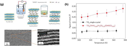
Figure 14. Ion doping in the energy fields. (a) Electrochemical process to dope LiCoO2 with Li vacancies [Citation24]. (b) The oxygen evolution reaction current as a function of applied potential [Citation24]. (c) The schematic figure of a fuel cell based on strongly correlated oxide, where hydrogen atom doped SmNiO3 serves as the electrolyte [Citation5]. (d) The current density-voltage behavior of a Pt/H-SNO/Pt-based SOFC at 500°C [Citation5]. (e) Schematic processes of doping the epitaxial VO2 on sapphire substrates through Pt assisted hydrogen doping. (f) Temperature dependent resistance measurements VO2 thin films with different level of hydrogen doping [Citation8]. (g) The experiments flow of how intercalation of organic molecules between the TiS2 layers [Citation25]. (h) Thermoelectric figure of merit (ZT) measurements of TiS2 single crystal and intercalated TiS2 as a function of temperature [Citation25]. Reproduced with permissions from Ref. [24] © Springer Nature 2014, Ref. [5] © Springer Nature 2016, Ref. [8] © Springer Nature 2016, Ref. [25] © Springer Nature 2015.
![Figure 14. Ion doping in the energy fields. (a) Electrochemical process to dope LiCoO2 with Li vacancies [Citation24]. (b) The oxygen evolution reaction current as a function of applied potential [Citation24]. (c) The schematic figure of a fuel cell based on strongly correlated oxide, where hydrogen atom doped SmNiO3 serves as the electrolyte [Citation5]. (d) The current density-voltage behavior of a Pt/H-SNO/Pt-based SOFC at 500°C [Citation5]. (e) Schematic processes of doping the epitaxial VO2 on sapphire substrates through Pt assisted hydrogen doping. (f) Temperature dependent resistance measurements VO2 thin films with different level of hydrogen doping [Citation8]. (g) The experiments flow of how intercalation of organic molecules between the TiS2 layers [Citation25]. (h) Thermoelectric figure of merit (ZT) measurements of TiS2 single crystal and intercalated TiS2 as a function of temperature [Citation25]. Reproduced with permissions from Ref. [24] © Springer Nature 2014, Ref. [5] © Springer Nature 2016, Ref. [8] © Springer Nature 2016, Ref. [25] © Springer Nature 2015.](/cms/asset/d7c8c12c-5a1b-4da4-9249-77db8c1fa0ff/tapx_a_1523686_f0014a_oc.jpg)
The improvement in catalytic activity for the delithiated compound (De-LiCoO2) over LiCoO2 is substantial, with a reduced onset potential of 1.52 V from 1.59 V and a large current increase (3.8 mA/cm2 vs. 2.3 mA/cm2) (red vs. black curves in )). Based on the Tafel slopes for both samples, this difference in onset potential is equivalent to an improvement in OER activity by a factor of 10. Lu et al. further tested the generality of the procedure on other LiCo alloys including LiCoO0.5Ni0.5O2 and LiCo0.5Fe0.5O2. The delithiated compound of LiCo0.33Ni0.33Fe0.33O2 exhibited the highest activities, with values comparable to the best OER catalysts yet discovered.
Figure 14. (Continued).
3.2.2 Hydrogen-doped fuel cell electrolytes
As described by Zhou et al. [Citation5], mixed conducting perovskites can be transformed into near unity-transference ionic conductors by proton incorporation, making them highly effective solid electrolytes. The design of a SNO based fuel cell (Pt/H-SNO/Pt) is shown in ), where hydrogen is exposed to the anode, dissociating into protons and electrons and creating Ni2+ at the SmNiO3 surface and triple phase boundaries (TPBs). This side of SmNiO3 (H-SNO) remains electronically insulating with hydrogen exposure, but H+ diffuses across the electrolyte due to the potential gradient while electrons bypass the electrolyte via an external circuit to generate power. Oxygen recombines with the protons at the cathode side, with H2O as a by-product. The current density-voltage behavior of a Pt/H-SNO/Pt-based SOFC at 500°C is shown in ). The corresponding power densities are shown by the solid lines for three different cells, with SmNiO3 thicknesses of 1.5 µm for cell 1 and 1.0 µm for cells 2 and 3. As seen, the maximum output is 225 mW/cm2 and is comparable to other high-performance proton conducting fuel cells in this temperature range [Citation130].
3.2.3 Chemical fuel storage
Yoon et al. reported changes in electronic structure via hydrogen doping in VO2 [Citation8]. VO2 is a correlated material that normally undergoes a metal-to-insulator transition around 68°C upon cooling, but the doping of hydrogen into the rutile interstices is known to stabilize the metallic phase down to room temperature [Citation9,Citation131]. Using Pt nanocatalysts in a hydrogen atmosphere, Yoon et al. were able to form a new, insulating HxVO2 phase, with the maximum value of x being 1 and thus suitable for hydrogen fuel storage. Furthermore, hydrogen could be fully removed from the epitaxial film, such that they could repeatedly demonstrate insulator-metal-insulator modulation. ) shows the system of 30-nm-thick epitaxial VO2 on either (0001) Al2O3 or (100) TiO2 substrates before and after the deposition of Pt nanocatalysts to dissociate H2. The samples were annealed at 120°C in forming gas, leading to hydrogen doping of the VO2.
The effect of hydrogen on the temperature-dependent conductivity is shown in ) for three different states. Results for the as-grown VO2 film are presented in plot I, exhibiting the well-known metal-to-insulator transition. As hydrogen enters VO2, electrons fill the V 3d orbitals (HxVO2), and the resistance decreases, leading to the behavior shown in plots II and III. As the amount of hydrogen doping reaches saturation in HVO2 (forming V3+ from V4+), the thin film becomes highly insulating across the temperature range, as shown in plot IV. The behavior is topotactic, in that the condition of the original VO2 lattice remains intact. As may be expected, the bandgap of HVO2 becomes large enough such that the film becomes slightly transparent. While full removal of hydrogen from HVO2 did not take place under ambient conditions, complete dehydrogenation could be achieved by annealing at higher temperatures.
3.2.4 Thermoelectrics design
Wan et al. reported an n-type organic semiconductor comprising the inorganic transition metal dichalcogenide, TiS2, and organic cations [Citation25]. The synthesis process is shown in ), using electrochemical intercalation and solvent exchange. Here, TiS2 single crystals were used as the cathode in electrochemical cells employing an organic electrolyte (here, hexylammonium chloride in dimethylsulphoxide). An applied potential leads to Ti3+ formation and negative charging of the TiS2 layers (left panel), causing the organic cations as well as solvent molecules in the electrolyte to intercalate between the TiS2 sheets (middle panel). Much of the DMSO molecules were then exchanged with H2O via the solvent exchange process; simultaneously, the HA ions transformed into a monolayer configuration (right panel). The resulting superlattice is stable up to 120°C and therefore suitable for room temperature applications. A high-angle annular dark-field scanning transmission electron microscopy image of the superlattice is shown on the bottom left of ), with a magnified image on the bottom right. The bright contrast stems from the TiS2 layers, and the superlattice period is 0.965 nm.
A comparison of the thermoelectric figures of merit for the superlattice and a TiS2 single crystal is shown in ). Despite the presence of interstitial Ti atoms and a high carrier concentration, the Seebeck coefficient was still relatively high for the dichalcogenide. As for the intercalated superlattice, the in-plane power factor (σS2) is lower than that of TiS2 but is higher than any other p-type flexible thermoelectric material. Most importantly, due to the organic component, the in-plane thermal conductivity of the superlattice is much lower than that of TiS2. This leads to a significant enhancement of the in-plane ZT, which is 0.28 at 100°C. This value is close to that of the best-known p-type organic material.
3.3 Iontronics in emerging research fields
The influence of iontronics on early stage fields such as neuromorphic computing, advanced spintronic and superconducting materials, as well as two-dimensional materials are reviewed.
3.3.1 Neuromorphic computing
The basic biological neural network in the brain comprises neurons that are connected by synapses in complex architectures ()). Information is transmitted from pre-neuron to post-neuron and scaled by the synapses, the weight of which can be updated by the time interval between post-neuron and pre-neuron signals [Citation132]. The neural network learns to perform a specific task by updating its synaptic weight. As a result, for the design of device networks similar to the neural network, one expects its basic units to both process signals and remember its training history simultaneously. Recent work presents new opportunities for using oxide quantum materials in neuromorphic computing using electrochemical ion doping. ) shows a schematic of three terminal synaptic transistor [Citation20]. The source and drain mimic the pre-neuron and post-neuron terminals, while the SmNiO3 perovskite oxide film acts as a channel material that can perform a computing task triggered by gate pulses. ) illustrates the conductance modulation mechanism of this device. Under positive gating, oxygen vacancies form in SmNiO3, leading to the reduction of Ni3+ to Ni2+ and an increase in resistivity. Under negative bias, oxygen is restored to SmNiO3, oxidizing Ni2+ to Ni3+, such that SmNiO3 recovers its low resistance state. ) shows that by applying a −2.5V pulse, the sheet conductance of device increases by 1,000% in 1,500 cycles. By reversing the bias pulse, the sheet conductance returns to the initial value in ~900 cycles. Such a device also exhibits both symmetric and asymmetric spike-timing-dependent plasticity behavior mimicking biological systems ()).
Figure 15. Iontronics in neuromorphic learning. (a–e) Three terminal synaptic transistor device based on perovskite nickelate (a–c), the synaptic properties of the device are shown in (d) and (e) [Citation20]. (f–h) The habituation behavior of quantum materials similar to that of organisms, see (f). The experimental observation of habituation phenomenon is shown in (g). (h) shows the recovery of original resistance state after air exposure for 12 h and then the habituation process can be reproduced [Citation29]. Reproduced with permissions from Ref. [20] © Springer Nature 2013, Ref. [29] © Springer Nature 2017.
![Figure 15. Iontronics in neuromorphic learning. (a–e) Three terminal synaptic transistor device based on perovskite nickelate (a–c), the synaptic properties of the device are shown in (d) and (e) [Citation20]. (f–h) The habituation behavior of quantum materials similar to that of organisms, see (f). The experimental observation of habituation phenomenon is shown in (g). (h) shows the recovery of original resistance state after air exposure for 12 h and then the habituation process can be reproduced [Citation29]. Reproduced with permissions from Ref. [20] © Springer Nature 2013, Ref. [29] © Springer Nature 2017.](/cms/asset/7c5924ab-eff0-4781-90d6-5b7c487a9d25/tapx_a_1523686_f0015_oc.jpg)
Iontronics based on perovskites further demonstrate the capability for habituation-based plasticity, which provides a new learning algorithm, adaptive synaptic plasticity, for neuromorphic computing. Zuo et al. utilized SmNiO3 thin films with catalytic electrodes deposited on the top and interfaced this device with a gas environment where the hydrogen concentration was controlled [Citation29]. As shown in ), after exposing the device to H2, hydrogen intercalates into the lattice as protons and a significant amount of Ni is reduced to Ni2+. Such an ion doping process results in doubly occupied Ni eg orbitals and electron localization. During subsequent H2 exposures with a short relaxation interval in a H2-free environment, more protons are doped into lattice but with slower kinetics and diminished conductance modulation ()), demonstrating a habituation behavior like that found in organisms, which is reproducible, see ). By incorporating the habituation-based plasticity, an efficient spiking neural network can be constructed without catastrophic forgetting. The key enablers for this result are the nonlinear changes in electrical resistance due to doping and ability to control binding of the dopant to the lattice.
3.3.2 Spintronic and superconducting devices
For copper and iron-based superconductors, carrier doping is critical to generate high Tc superconductivity and restrain magnetic ordering [Citation133,Citation134]. Chemical substitution of elements with ones of dissimilar valence has been utilized to modulate the carrier type and concentration; this process is mostly irreversible and constrained by chemical solubility. Using an electric field with an ionic liquid in the EDLT geometry is another approach for modulating carriers in superconducting materials [Citation2], but carrier accumulation in the electrostatic gating region is inefficient in some materials (e.g. MoTe2) for inducing superconductivity [Citation135]. Recently, Shi et al. reported that under a large bias and using a KClO4/polyethylene glycol electrolyte, a electrochemical reaction between the electrolyte and channel material can occur, resulting in bulk ionic doping and an accumulation of carriers far beyond the level of electrostatic surface doping, leading to the observation of superconductivity in MoTe2 [Citation135]. Cui et al. further utilized protonation process to induce the high Tc phase in iron-based superconductors [Citation26]. The proton doping process and setup are illustrated in ]. A FeSeS single crystal is connected with a Pt electrode with a 3V voltage source, and the gap between them is filled with an ionic liquid (DEME-TFSI and FMIM-BF4) that contains water. The DC susceptibility of FeSe0.93S0.07 after protonation for six days is shown in ). Tc1 (~9 K) corresponds to the superconducting transition of non-protonated region, while for protonated region the superconducting transition appears at a higher temperature, Tc2 (~42.5 K). These recent achievements suggest that iontronics that enable higher levels of carrier doping can be relevant for the development and study of superconducting materials.
Figure 16. Effect of ion doping in superconductivity, spintronics, and two-dimensional materials. (a–b) Protonation induced superconductivity modulation in FeSe2 single crystal, where the setup for proton doping is shown in (a) and the higher superconducting transition temperature after protonation can be observed in (b) [Citation26]. (c–d) Spin orbit torque tuned by oxygen manipulation. (c) Film structure where SiO2 capping layer control the oxygen level of the device. The switching of Hall resistance ~ in-plane current curve with reducing capping layer thickness is shown in (d) [Citation16]. (e–g) Cu doping induced transparency in Bi2Se3 nanoplates, where the Cu is doped into gap between the two-dimensional layers (e). (f) and (g) show the transmission optical image of Bi2Se3 nanoplate before and after doping [Citation21]. (h–i) Li-ion-doping induced electronic ground state variation of layer-structured 1T-TaS2 thin flakes. (h) Schematic setup of 1T-TaS2 ionic field effect transistor for Li doping. (i) Li-doping induced phase evolution in 1T-TaS2 thin flakes in three thickness regions [Citation30]. Reproduced with permissions from Ref. [26] © Elsevier 2018, Ref. [16] © Springer Nature 2015, Ref. [21] © Springer Nature 2014, Ref. [30] © Springer Nature 2015.
![Figure 16. Effect of ion doping in superconductivity, spintronics, and two-dimensional materials. (a–b) Protonation induced superconductivity modulation in FeSe2 single crystal, where the setup for proton doping is shown in (a) and the higher superconducting transition temperature after protonation can be observed in (b) [Citation26]. (c–d) Spin orbit torque tuned by oxygen manipulation. (c) Film structure where SiO2 capping layer control the oxygen level of the device. The switching of Hall resistance ~ in-plane current curve with reducing capping layer thickness is shown in (d) [Citation16]. (e–g) Cu doping induced transparency in Bi2Se3 nanoplates, where the Cu is doped into gap between the two-dimensional layers (e). (f) and (g) show the transmission optical image of Bi2Se3 nanoplate before and after doping [Citation21]. (h–i) Li-ion-doping induced electronic ground state variation of layer-structured 1T-TaS2 thin flakes. (h) Schematic setup of 1T-TaS2 ionic field effect transistor for Li doping. (i) Li-doping induced phase evolution in 1T-TaS2 thin flakes in three thickness regions [Citation30]. Reproduced with permissions from Ref. [26] © Elsevier 2018, Ref. [16] © Springer Nature 2015, Ref. [21] © Springer Nature 2014, Ref. [30] © Springer Nature 2015.](/cms/asset/abdc2009-07ee-48aa-a6a5-2c00f48002d5/tapx_a_1523686_f0016_oc.jpg)
Aside from applications in superconductivity, iontronics can also be applied to spintronic devices. Recent work by Qiu et al. showed that spin-orbit-torque can be engineered by oxygen manipulation [Citation16]. The device utilized in this work is shown in ) as Pt/CoFeB/MgO/SiO2 thin films deposited by sputtering [Citation16]. The thickness of the SiO2 capping layer is varied to control the oxygen level of the layer structure. With a thinner layer of SiO2, oxygen can diffuse into CoFeB layer through the SiO2 and MgO layers. ) shows that by reducing the thickness of SiO2, i.e. increasing oxygen level, switching of the Hall resistance (RH) as a function of in-plane current I can be changed from clockwise (as guided by arrows) in a 3-nm-thick SiO2 device to anticlockwise in a SiO2-free device. Although in this work the oxygen level of the devices is controlled in an irreversible way (changing the capping layer thickness), it clearly shows the advantages of utilizing ions in spintronics and further indicates the possibility of achieving reversible manipulation of spin transport through devices designed to exploit controllable ion motion (such as the methods discussed in Section 2).
3.3.3 Electrochemical design of two-dimensional materials
Layered two-dimensional materials, such as graphene, black phosphorus, boron nitride, and metal chalcogenides have drawn great attention due to their variety of novel and interesting chemical and physical properties with potential applications in optoelectronics, field effect transistors, electro-catalysts, topological insulators, and thermoelectrics. These two-dimensional materials possess strong covalent bonds between the atoms within each layer and weak van der Waals interactions between the layers. Due to this weak interaction, two-dimensional materials are highly tolerant of ion doping [Citation136,Citation137]. A large volumetric capacitance of cations including Na+, K+, NH4+, Mg2+, and Al3+ was reported for two-dimensional titanium carbide, which is more than 300 F per cubic centimeter (higher than porous carbon) [Citation138]. The ion doping of two-dimensional materials has been achieved by both chemical and electrochemical methods, where the latter one offers reversible ion motion and is also closely related to switchable device applications.
,,) show experimental results from Yao et al. on a chemical doping induced change of optical properties of a Bi2Se3 nanoplate [Citation21]. Bi2Se3 is a two-dimensional material with unique thermoelectric behavior and was shown to be a topological insulator [Citation139]. As ) shows, Yao et al. intercalated Cu into the van der Waals gap of Bi2Se3 by adding the nanoplate to a mixture of 5 ml butanol and 3 mg [Cu(CH3CN)4]PF6 and heating the mixture to 55°C. show the optical transmission image of the same Bi2Se3 nanoplate (~8 nm) before and after Cu intercalation for 1 h, with the nanoplate becoming much more transparent after Cu intercalation. Besides tuning the optical properties of two dimensional materials, Mouri et al. also reported the modulation of photoluminescence in a monolayer of MoS2 by chemical doping of the p-type dopants, F2TCNQ and TCNQ [Citation140]. Ion doping has also been used to control the competition, cooperation, and coexistence of collectively ordered electronic states of two-dimensional systems. and 16(i) demonstrate tuning of the electronic ground state of the layered crystal 1T-TaS2 by gate-controlled Li ion intercalation through a ionic field effect transistor device structure [Citation30]. The gate medium is a gel-like solid electrolyte with LiClO4 dissolved in polyethylene oxide; the Li ions can move in and out of the 1T-TaS2 channels under electric field. ) shows the phase diagram of the 1T-TaS2 flakes under doping in three thickness regimes, clearly demonstrating the rich electronic states among the incommensurate charge density wave (ICCDW), textured nearly commensurate CDW (NCCDW), commensurate CDW (CCDW), superconducting (SC), and insulator by Li ion doping in all samples. These interesting results suggest that ion doping is a promising approach for the study of two-dimensional materials, also indicates a bright future of materials discovery and device innovation in the regime of extreme doping -).
4 Future research needs
We have summarized ion-electron doping mechanisms and recent efforts to discover functionalities and design new phases in solid materials via ion doping through soft interfaces (gas, liquid) and solid electrolytes/ionic reservoirs. A few mechanisms are common to these studies: extreme carrier doping via intercalation of ions beyond the electrostatic effect, re-arrangement of the lattice structure due to extreme ion doping, and giant strain development that can distort lattice symmetry and/or split electron energy levels. Most interestingly, the use of electric fields makes these modifications reversible, non-volatile and doping at distinct levels can be achieved. Such capabilities open up completely new areas for scholarship in materials science and associated fields such as condensed matter physics and electrochemistry, as well as applications in several societal-relevant technologies.
While already impressive proof-of-concept demonstrations in a range of fields have been reported to date, much work remains. For instance, theoretical guidance to understand the atomistic pathways governing the structural modifications is needed. First principles calculations of ion doping effects have been carried out in recent studies through incorporation of charge with a compensating background or the dopants [Citation3,Citation4,Citation141]. These studies show the strain evolution due to doping and gap changes, and provide microscopic understanding of the physics. Defect calculations involving large unit cells will be required in future to understand how the band structure evolves as a function of defect concentration. Molecular dynamics simulations are useful to understand the kinetics and diffusion pathways. Free energy calculations of different metastable phases that form at different doping levels however are as yet unknown. To what extent a lattice can hold such large amounts of charges and dopants without transforming into another phase is material dependent, and general principles for different crystal structures or anisotropic behavior within a lattice type are warranted. Electric-field driven diffusion is a key aspect to several of these approaches, however, kinetic parameters for diffusivity and mathematical models for percolative transport across regions of distinct conductivity remain largely unexplored. Theoretical treatments of phase transforming materials under strong electric fields will enormously help understand and guide experimental work.
Electrochromic smart windows are among the leading technologies that may be impacted in the near-term, while in the longer term, brain-like circuits and non-volatile memory would likely be interesting application areas. The limits of small-ion mobility in various lattices should be studied as well as the reliability and thermal tolerances of devices exploiting such operational mechanisms. Machine learning techniques that are increasingly adopted to guide synthesis of new materials could be explored in this field to identify systems with tunable fragile band structures or materials on the cusp of phase transitions. Such studies could pose ionic doping and the coupling of charge carriers with the lattice as a powerful new approach to design functional materials that can evolve, be aware of training history or experience, are environmentally adaptive and can learn. Such evolvable devices may represent a new paradigm for solid state and hybrid liquid-solid phase devices of the 21st century in information processing, synthetic analogs for neuroscience research and energy transfer.
Disclosure statement
No potential conflict of interest was reported by the authors.
Additional information
Funding
References
- D.D. Fong and S. Ramanathan, APL Mater. 5 (2017) p. 1. doi:10.1063/1.4982238
- S.Z. Bisri, S. Shimizu, M. Nakano and Y. Iwasa, Adv. Mater. 29 (2017) p. 1–42. doi:10.1002/adma.201700681
- N. Lu, P. Zhang, Q. Zhang, R. Qiao, Q. He, H.B. Li, Y. Wang, J. Guo, D. Zhang, Z. Duan, Z. Li, M. Wang, S. Yang, M. Yan, E. Arenholz, S. Zhou, W. Yang, L. Gu, C.W. Nan, J. Wu, Y. Tokura and P. Yu, Nature. 546 (2017) p. 124–128. doi:10.1038/nature22389
- Z. Zhang, D. Schwanz, B. Narayanan, M. Kotiuga, J.A. Dura, M. Cherukara, H. Zhou, J.W. Freeland, J. Li, R. Sutarto, F. He, C. Wu, J. Zhu, Y. Sun, K. Ramadoss, S.S. Nonnenmann, N. Yu, R. Comin, K.M. Rabe, S.K.R.S. Sankaranarayanan and S. Ramanathan, Nature. 553 (2017) p. 68–72. doi:10.1038/nature25008
- Y. Zhou, X. Guan, H. Zhou, K. Ramadoss, S. Adam, H. Liu, S. Lee, J. Shi, M. Tsuchiya, D.D. Fong and S. Ramanathan, Nature. 534 (2016) p. 231–234. doi:10.1038/nature17653
- D.A. Gilbert, J. Olamit, R.K. Dumas, B.J. Kirby, A.J. Grutter, B.B. Maranville, E. Arenholz, J.A. Borchers and K. Liu, Nat. Commun. 7 (2016) p. 11050. doi:10.1038/ncomms11050
- H.-B. Li, N. Lu, Q. Zhang, Y. Wang, D. Feng, T. Chen, S. Yang, Z. Duan, Z. Li, Y. Shi, W. Wang, W.-H. Wang, K. Jin, H. Liu, J. Ma, L. Gu, C. Nan and P. Yu, Nat. Commun. 8 (2017) p. 2156. doi:10.1038/s41467-017-02359-6
- H. Yoon, M. Choi, T.-W. Lim, H. Kwon, K. Ihm, J.K. Kim, S.-Y. Choi and J. Son, Nat. Mater. 15 (2016) p. 1113–1119. doi:10.1038/nmat4692
- J. Wei, H. Ji, W. Guo, A.H. Nevidomskyy and D. Natelson, Nat. Nanotechnol. 7 (2012) p. 357–362. doi:10.1038/nnano.2012.70
- H. Ji, J. Wei and D. Natelson, Nano Lett. 12 (2012) p. 2988–2992. doi:10.1021/nl300741h
- M. Li, W. Han, X. Jiang, J. Jeong, M.G. Samant and S.S.P. Parkin, Nano Lett. 13 (2013) p. 4675–4678. doi:10.1021/nl402088f
- T. Onozuka, A. Chikamatsu, T. Katayama, Y. Hirose, I. Harayama, D. Sekiba, E. Ikenaga, M. Minohara, H. Kumigashira and T. Hasegawa, ACS Appl. Mater. Interfaces. 9 (2017) p. 10882–10887. doi:10.1021/acsami.7b00855
- H.-T. Zhang, L. Guo, G. Stone, L. Zhang, Y.-X. Zheng, E. Freeman, D.W. Keefer, S. Chaudhuri, H. Paik, J.A. Moyer, M. Barth, D.G. Schlom, J. V Badding, S. Datta, V. Gopalan and R. Engel-Herbert, Adv. Funct. Mater. 26 (2016) p. 6612–6618. doi:10.1002/adfm.201601890
- S.-I. Ohkoshi, K. Nakagawa, K. Tomono, K. Imoto, Y. Tsunobuchi and H. Tokoro, J. Am. Chem. Soc. 132 (2010) p. 6620–6621. doi:10.1021/ja100385f
- H.-T. Zhang, L. Zhang, D. Mukherjee, Y.-X. Zheng, R.C. Haislmaier, N. Alem amd R. Engel-Herbert, Nat. Commun. 6 (2015) p. 8475. doi:10.1038/ncomms9475
- X. Qiu, K. Narayanapillai, Y. Wu, P. Deorani, D.-H. Yang, W.-S. Noh, J.-H. Park, K.-J. Lee, H.-W. Lee and H. Yang, Nat. Nanotechnol. 10 (2015) p. 333–338. doi:10.1038/nnano.2015.18
- J. Shi, Y. Zhou and S. Ramanathan, Nat. Commun. 5 (2014) p. 4860. doi:10.1038/ncomms5972
- M. Imada, A. Fujimori and Y. Tokura, Rev. Mod. Phys. 70 (1998) p. 1039–1263.
- L. Baldrati, A.J. Tan, M. Mann, R. Bertacco and G.S.D. Beach, Appl. Phys. Lett. 110 (2017) p. 012404. doi:10.1063/1.4973475
- J. Shi, S.D. Ha, Y. Zhou, F. Schoofs and S. Ramanathan, Nat. Commun. 4 (2013) p. 2676. doi:10.1038/ncomms3676
- J. Yao, K.J. Koski, W. Luo, J.J. Cha, L. Hu, D. Kong, V.K. Narasimhan, K. Huo and Y. Cui, Nat. Commun. 5 (2014) p. 5670. doi:10.1038/ncomms5972
- U. Bauer, L. Yao, A.J. Tan, P. Agrawal, S. Emori, H.L. Tuller, S. Van Dijken and G.S.D. Beach, Nat. Mater. 14 (2015) p. 174–181. doi:10.1038/nmat4134
- X. Qiu, K. Narayanapillai, Y. Wu, P. Deorani, D.-H. Yang, W.-S. Noh, J.-H. Park, K.-J. Lee, H.-W. Lee and H. Yang, Nat. Nanotechnol. 10 (2015) p. 333–338. doi:10.1038/nnano.2015.18
- Z. Lu, H. Wang, D. Kong, K. Yan, P.C. Hsu, G. Zheng, H. Yao, Z. Liang, X. Sun and Y. Cui, Nat. Commun. 5 (2014) p. 4345. doi:10.1038/ncomms5972
- C. Wan, X. Gu, F. Dang, T. Itoh, Y. Wang, H. Sasaki, M. Kondo, K. Koga, K. Yabuki, G.J. Snyder, R. Yang and K. Koumoto, Nat. Mater. 14 (2015) p. 622. doi:10.1038/nmat4251
- Y. Cui, G. Zhang, H. Li, H. Lin, X. Zhu, H.-H. Wen, G. Wang, J. Sun, M. Ma, Y. Li, Dongliang Gongf, T. Xie, Y. Gu, S. Lie, H. Luo, P. Yu and W. Yu, Sci. Bull. 63 (2017) p. 11–16. doi:10.1016/j.scib.2017.12.009
- D.R. Rosseinsky and R.J. Mortimer, Adv. Mater. 13 (2001) p. 783–793. doi:10.1002/1521-4095(200106)13:11<783::AID-ADMA783>3.0.CO;2-D
- P.R. Pudasaini, J.H. Noh, A.T. Wong, O.S. Ovchinnikova, A. V. Haglund, S. Dai, T.Z. Ward, D. Mandrus and P.D. Rack, Adv. Funct. Mater. 26 (2016) p. 2820–2825. doi:10.1002/adfm.201505274
- F. Zuo, P. Panda, M. Kotiuga, J. Li, M. Kang, C. Mazzoli, H. Zhou, A. Barbour, S. Wilkins, B. Narayanan, M. Cherukara, Z. Zhang, S.K.R.S. Sankaranarayanan, R. Comin, K.M. Rabe, K. Roy and S. Ramanathan, Nat. Commun. 8 (2017) p. 240. doi:10.1038/s41467-017-00248-6
- Y. Yu, F. Yang, X.F. Lu, Y.J. Yan, Y.-H. Cho, L. Ma, X. Niu, S. Kim, Y.-W. Son, D. Feng, Shiyan Li, S.-W. Cheong, X.H. Chen and Y. Zhang, Nat. Nanotechnol. 10 (2015) p. 270–276. doi:10.1038/nnano.2014.323
- C. Oh, S. Heo, H.M. Jang and J. Son, Appl. Phys. Lett. 108 (2016) p. 122106. doi:10.1063/1.4944842
- Y. Zhou, J. Park, J. Shi, M. Chhowalla, H. Park, D.A. Weitz and S. Ramanathan, Nano Lett. 15 (2015) p. 1627–1634. doi:10.1021/nl504066f
- K. Yoshimatsu, M. Niwa, H. Mashiko, T. Oshima and A. Ohtomo, Sci. Rep. 5 (2015) p. 16325. doi:10.1038/srep16325
- T.D. Schladt, T. Graf, N.B. Aetukuri, M. Li, A. Fantini, X. Jiang, M.G. Samant and S.S.P. Parkin, ACS Nano. 7 (2013) p. 8074–8081. doi:10.1021/nn305697q
- T. Katase, Y. Suzuki and H. Ohta, Adv. Electron. Mater. 2 (2016) p. 1600044. doi:10.1002/aelm.201600044
- T. Ichimura, K. Fujiwara and H. Tanaka, Sci. Rep. 4 (2014) p. 5818. doi:10.1038/srep05818
- J. Jeong, N. Aetukuri, T. Graf, T.D. Schladt, M.G. Samant and S.S.P. Parkin, Science. 339 (2013) p. 1402–1405. doi:10.1126/science.1230512
- S.H. Skjærvø, E.T. Wefring, S.K. Nesdal, N.H. Gaukås, G.H. Olsen, J. Glaum, T. Tybell and S.M. Selbach, Nat. Commun. 7 (2016) p. 13745. doi:10.1038/ncomms13745
- W.-K. Hong, J.B. Park, J. Yoon, B.-J. Kim, J.I. Sohn, Y.B. Lee, T.-S. Bae, S.-J. Chang, Y.S. Huh, B. Son, E.A. Stach, T. Lee and M.E. Welland, Nano Lett. 13 (2013) p. 1822–1828. doi:10.1021/nl400511x
- L. Malavasi, M.C. Mozzati, C.B. Azzoni, G. Chiodelli and G. Flor, Solid State Commun. 123 (2002) p. 321–326. doi:10.1016/S0038-1098(02)00376-9
- V.N. Andreev, V.A. Klimov and M.E. Kompan, Phys. Solid State. 54 (2012) p. 601–606. doi:10.1134/S1063783412030043
- M. Tsuchiya, S.K.R.S. Sankaranarayanan and S. Ramanathan, Prog. Mater. Sci. 54 (2009) p. 981–1057. doi:10.1016/j.pmatsci.2009.04.003
- S.D. Ha, U. Vetter, J. Shi and S. Ramanathan, Appl. Phys. Lett. 102 (2013) p. 183102. doi:10.1063/1.4804142
- K. Fujiwara, T. Ichimura and H. Tanaka, Adv. Mater. Interfaces. 1 (2014) p. 1300108. doi:10.1002/admi.201300108
- T. Kanki and H. Tanaka, APL Mater. 5 (2017) p. 042303. doi:10.1063/1.4974484
- H. Ohta, Y. Sato, T. Kato, S. Kim, K. Nomura, Y. Ikuhara and H. Hosono, Nat. Commun. 1 (2010) p. 118. doi:10.1038/ncomms1112
- T. Sasaki, H. Ueda, T. Kanki and H. Tanaka, Sci. Rep. 5 (2015) p. 17080. doi:10.1038/srep17080
- F. Lin, Y. Liu, X. Yu, L. Cheng, A. Singer, O.G. Shpyrko, H.L. Xin, N. Tamura, C. Tian, T.C. Weng, X.Q. Yang, Y.S. Meng, D. Nordlund, W. Yang and M.M. Doeff, Chem. Rev. 117 (2017) p. 13123–13186. doi:10.1021/acs.chemrev.7b00024
- H. Zhou and D.D. Fong, In Situ X-Ray Scattering of Epitaxial Oxide Thin Films. Epitaxial Growth of Complex Metal Oxides, Woodhead Publishing, Cambridge, UK, 2015. doi:10.1016/B978-1-78242-245-7.00010-5
- M. Eriksson, J.F. Van Der Veen and C. Quitmann, J. Synchrotron Radiat. 21 (2014) p. 837–842. doi:10.1107/S1600577514019286
- J. Jeong, N.B. Aetukuri, D. Passarello, S.D. Conradson, M.G. Samant and S.S.P. Parkin, Proc. Natl. Acad. Sci. 112 (2015) p. 1013–1018. doi:10.1073/pnas.1419051112
- Y. Dong, H. Xu, Z. Luo, H. Zhou, D.D. Fong, W. Wu and C. Gao, APL Mater. 5 (2017) p. 051101. doi:10.1063/1.4983617
- J. Walter, G. Yu, B. Yu, A. Grutter, B. Kirby, J. Borchers, Z. Zhang, H. Zhou, T. Birol, M. Greven and C. Leighton, Phys. Rev. Mater. 1 (2017) p. 071403. doi:10.1103/PhysRevMaterials.1.071403
- D. Marrocchelli, N.H. Perry and S.R. Bishop, Phys. Chem. Chem. Phys. 17 (2015) p. 10028–10039. doi:10.1039/C4CP05885B
- S.R. Bishop, D. Marrocchelli, C. Chatzichristodoulou, N.H. Perry, M.B. Mogensen, H.L. Tuller and E.D. Wachsman, Annu. Rev. Mater. Res. 44 (2014) p. 205–239. doi:10.1146/annurev-matsci-070813-113329
- Z. Feng, Y. Yacoby, W.T. Hong, H. Zhou, M.D. Biegalski, H.M. Christen and Y. Shao-Horn, Energy Environ. Sci. 7 (2014) p. 1166. doi:10.1039/c3ee43164a
- D.D. Fong and C. Lucas, MRS Bull. 35 (2010) p. 504–513. doi:10.1557/mrs2010.599
- Y. Yacoby, M. Sowwan, E. Stern, J.O. Cross, D. Brewe, R.O.N. Pindak, J. Pitney, E.M. Dufresne and R.O.Y. Clarke, Nat. Mater. 1 (2002) p. 99–101. doi:10.1038/nmat735
- H. Zhou, Y. Yacoby, V.Y. Butko, G. Logvenov, I. Bozovic and R. Pindak, Proc. Natl. Acad. Sci. USA. 107 (2010) p. 8103–8107. doi:10.1073/pnas.0910097107
- T.T. Fister, H. Zhou, Z. Luo, S.S.A. Seo, S.O. Hruszkewycz, D.L. Proffit, J.A. Eastman, P.H. Fuoss, P.M. Baldo, H.N. Lee and D.D. Fong, APL Mater. 2 (2014) p. 021102. doi:10.1063/1.4865160
- S. Kumar, C.E. Graves, J.P. Strachan, E.M. Grafals, A.L.D. Kilcoyne, T. Tyliszczak, J.N. Weker, Y. Nishi and R.S. Williams, Adv. Mater. 28 (2016) p. 2772–2776. doi:10.1002/adma.201505435
- J.J. Yang, D.B. Strukov and D.R. Stewart, Nat. Nanotechnol. 8 (2013) p. 13–24. doi:10.1038/nnano.2012.240
- S. Kumar, C.E. Graves, J.P. Strachan, A.L.D. Kilcoyne, T. Tyliszczak, Y. Nishi and R.S. Williams, J. Appl. Phys. 118 (2015) p. 034502. doi:10.1063/1.4926477
- M. Holt, R. Harder, R. Winarski and V. Rose, Annu. Rev. Mater. Res. 43 (2013) p. 183–211. doi:10.1146/annurev-matsci-071312-121654
- P. Fenter, C. Park, Z. Zhang and S. Wang, Nat. Phys. 2 (2006) p. 2–6. doi:10.1038/nphys419
- N. Laanait, Z. Zhang, C.M. Schlepütz, J. Vila-Comamala, M.J. Highland and P. Fenter, J. Synchrotron Radiat. 21 (2014) p. 1252–1261. doi:10.1107/S1600577514016555
- N. Laanait, E.B.R. Callagon, Z. Zhang, N.C. Sturchio, S.S. Lee and P. Fenter, Science. 349 (2015) p. 1330. doi:10.1126/science.aab3272
- N. Laanait, W. Saenrang, H. Zhou, C. Eom and Z. Zhang, Adv. Struct. Chem. Imaging. 3 (2017) p. 11. doi:10.1186/s40679-017-0044-3
- A.P. Hitchcock and M.F. Toney, J. Synchrotron Radiat. 21 (2014) p. 1019–1030. doi:10.1107/S1600577514013046
- A.I. Frenkel and J.A. Van Bokhoven, J. Synchrotron Radiat. 21 (2014) p. 1084–1089. doi:10.1107/S1600577514014854
- P. Thibault, M. Guizar-Sicairos and A. Menzel, J. Synchrotron Radiat. 21 (2014) p. 1011–1018. doi:10.1107/S1600577514015343
- J. Miao, T. Ishikawa, I.K. Robinson and M.M. Murnane, Science. 348 (2015) p. 249–254. doi:10.1126/science.aaa5139
- I. Robinson and R. Harder, Nat. Mater. 8 (2009) p. 291–298. doi:10.1038/nmat2400
- B. Abbey, JOM. 65 (2013) p. 1183–1201. doi:10.1007/s11837-013-0702-4
- A. Yau, W. Cha, M.W. Kanan, G.B. Stephenson and A. Ulvestad, Science. 742 (2017) p. 739–742. doi:10.1126/science.aam6168
- A. Ulvestad, A. Singer, J.N. Clark, H.M. Cho, J.W. Kim, R. Harder, J. Maser, Y.S. Meng and O.G. Shpyrko, Science. 1344 (2015) p. 1344–1348. doi:10.1126/science.aaa1313
- A. Ulvestad, Y. Nashed, G. Beutier, M. Verdier, S.O. Hruszkewycz and M. Dupraz, Sci. Rep. 7 (2017) p. 9920. doi:10.1038/s41598-017-09582-7
- K.M. Pavlov, V.I. Punegov, K.S. Morgan, G. Schmalz and D.M. Paganin, Sci. Rep. 7 (2017) p. 1132. doi:10.1038/s41598-017-01164-x
- F. Hofmann, E. Tarleton, R.J. Harder, N.W. Phillips, P.W. Ma, J.N. Clark, I.K. Robinson, B. Abbey, W. Liu and C.E. Beck, Sci. Rep. 7 (2017) p. 45993. doi:10.1038/srep45993
- O.G. Shpyrko, J. Synchrotron Radiat. 21 (2014) p. 1057–1064. doi:10.1107/S1600577514018232
- M.S. Pierce, K.C. Chang, D. Hennessy, V. Komanicky, M. Sprung, A. Sandy and H. You, Phys. Rev. Lett. 103 (2009) p. 165501. doi:10.1103/PhysRevLett.103.165501
- S.K. Sinha, Z. Jiang and L.B. Lurio, Adv. Mater. 26 (2014) p. 7764–7785. doi:10.1002/adma.201402404
- Q. Zhang, E.M. Dufresne, P. Chen, J. Park, M.P. Cosgriff, M. Yusuf, Y. Dong, D.D. Fong, H. Zhou, Z. Cai, R.J. Harder, S.J. Callori, M. Dawber, P.G. Evans, and A.R. Sandy, Phys. Rev. Lett. 118 (2017) p. 097601. doi:10.1103/PhysRevLett.118.097601
- S.V. Kalinin, A. Borisevich and D. Fong, ACS Nano. 6 (2012) p. 10423–10437. doi:10.1021/nn304930x
- R. Aso, D. Kan, Y. Shimakawa and H. Kurata, Sci. Rep. 3 (2013) p. 2214. doi:10.1038/srep02214
- A.Y. Borisevich, H.J. Chang, M. Huijben, M.P. Oxley, S. Okamoto, M.K. Niranjan, J.D. Burton, E.Y. Tsymbal, Y.H. Chu, P. Yu, R. Ramesh, S.V. Kalinin and S.J. Pennycook, Phys. Rev. Lett. 105 (2010) p. 87204. doi:10.1103/PhysRevLett.105.087204
- C.L. Jia and K. Urban, Science. 303 (2004) p. LP–2004. doi:10.1126/science.1093617
- Q. Zhang, X. He, J. Shi, N. Lu, H. Li, Q. Yu, Z. Zhang, L.-Q. Chen, B. Morris, Q. Xu, P. Yu, L. Gu, K. Jin and C.-W. Nan, Nat. Commun. 8 (2017) p. 104. doi:10.1038/s41467-017-00121-6
- J.H. Jang, Y.-M. Kim, Q. He, R. Mishra, L. Qiao, M.D. Biegalski, A.R. Lupini, S.T. Pantelides, S.J. Pennycook, S.V. Kalinin and A.Y. Borisevich, ACS Nano. 11 (2017) p. 6942–6949. doi:10.1021/acsnano.7b02188
- B. Cui, P. Werner, T. Ma, X. Zhong, Z. Wang, J.M. Taylor, Y. Zhuang and S.S.P. Parkin, Nat. Commun. 9 (2018) p. 3055. doi:10.1038/s41467-018-05330-1
- D.A. Bonnell, S.V. Kalinin, A.L. Kholkin and A. Gruverman, MRS Bull. 34 (2009) p. 648–657. doi:10.1557/mrs2009.176
- A. Kumar, F. Ciucci, A.N. Morozovska, S.V. Kalinin and S. Jesse, Nat. Chem. 3 (2011) p. 707. doi:10.1038/nchem.1112
- Y. Sharma, J. Balachandran, C. Sohn, J.T. Krogel, P. Ganesh, L. Collins, A. V Ievlev, Q. Li, X. Gao, N. Balke, O.S. Ovchinnikova, S. V Kalinin, O. Heinonen and H.N. Lee, ACS Nano. 12 (2018) p. 7159–7166. doi:10.1021/acsnano.8b03031
- S. Jesse, A. Kumar, T.M. Arruda, Y. Kim, S. V Kalinin and F. Ciucci, MRS Bull. 37 (2012) p. 651–658. doi:10.1557/mrs.2012.144
- S.V. Kalinin and N. Balke, Adv. Mater. 22 (2010) p. E193–E209. doi:10.1002/adma.201001190
- S.M. Yang, S. Lee, J. Jian, W. Zhang, P. Lu, Q. Jia, H. Wang, T. Won Noh, S. V Kalinin and J.L. MacManus‐Driscoll, Nat. Commun. 6 (2015) p. 8588. doi:10.1038/ncomms9588
- C. Leon, J. Santamaria and B.A. Boukamp, MRS Bull. 38 (2013) p. 1056–1063. doi:10.1557/mrs.2013.264
- S. Lee, W. Zhang, F. Khatkhatay, H. Wang, Q. Jia and J.L. MacManus-Driscoll, Nano Lett. 15 (2015) p. 7362–7369. doi:10.1021/nl504066f
- L. Zhang, Y. Zhou, L. Guo, W. Zhao, A. Barnes, H.-T. Zhang, C. Eaton, Y. Zheng, M. Brahlek, H.F. Haneef, N.J. Podraza, M.H.W. Chan, V. Gopalan, K.M. Rabe and R. Engel-Herbert, Nat. Mater. 15 (2016) p. 204–210. doi:10.1038/nmat4493
- H.-T. Zhang, M.J. Brahlek, X. Ji, S. Lei, J. Lapano, J.W. Freeland, V. Gopalan and R. Engel-Herbert, ACS Appl. Mater. Interfaces. 9 (2017) p. 12556–12562. doi:10.1021/acsami.6b16007
- M. Brahlek, L. Zhang, J. Lapano, H.-T. Zhang, R. Engel-Herbert, N. Shukla, S. Datta, H. Paik and D.G. Schlom, MRS Commun. 7 (2017) p. 27–52. doi:10.1557/mrc.2017.2
- M. Brahlek, L. Zhang, H.-T. Zhang, J. Lapano, L.R. Dedon, L.W. Martin and R. Engel-Herbert, Appl. Phys. Lett. 109 (2016) p. 101903. doi:10.1063/1.4962388
- C. Bi, Y. Liu, T. Newhouse-Illige, M. Xu, M. Rosales, J.W. Freeland, O. Mryasov, S. Zhang, S.G.E. Te Velthuis and W.G. Wang, Phys. Rev. Lett. 113 (2014) p. 267202. doi:10.1103/PhysRevLett.113.267202
- U. Bauer, L. Yao, A.J. Tan, P. Agrawal, S. Emori, H.L. Tuller, S. Van Dijken and G.S.D. Beach, Nat. Mater. 14 (2015) p. 174–181. doi:10.1038/nmat4134
- R. Waser and M. Aono, Nat. Mater. 6 (2007) p. 833–840. doi:10.1038/nmat2023
- H. Yuan, H. Shimotani, J. Ye, S. Yoon, H. Aliah, A. Tsukazaki, M. Kawasaki and Y. Iwasa, J. Am. Chem. Soc. 132 (2010) p. 18402–18407. doi:10.1021/ja108912x
- T. Ichimura, K. Fujiwara and H. Tanaka, Sci. Rep. 4 (2014) p. 5818. doi:10.1038/srep05818
- K. Ramadoss, F. Zuo, Y. Sun, Z. Zhang, J. Lin, U. Bhaskar, S.H. Shin, M.A. Alam, S. Guha, D. Weinstein and S. Ramanathan, IEEE Electron Device Lett. 1 (2018) doi:10.1109/LED.2018.2865776
- B. Zhu and B.-E. Mellander, Solid State Ionics. 97 (1997) p. 535–540. doi:10.1016/S0167-2738(97)00057-X
- Z. Li, Y. Zhou, H. Qi, Q. Pan, Z. Zhang, N.N. Shi, M. Lu, A. Stein, C.Y. Li, S. Ramanathan and N. Yu, Adv. Mater. 28 (2016) p. 9117–9125. doi:10.1002/adma.201601204
- S.-H. Lee, R. Deshpande, P.A. Parilla, K.M. Jones, B. To, A.H. Mahan and A.C. Dillon, Adv. Mater. 18 (2006) p. 763–766. doi:10.1002/adma.200501953
- Z. Zhang, F. Zuo, C. Wan, A. Dutta, J. Kim, J. Rensberg, R. Nawrodt, H.H. Park, T.J. Larrabee, X. Guan, You Zhou, S.M. Prokes, C. Ronning, A.B. Vladimir M. Shalaev, M.A. Kats and S. Ramanathan, Phys. Rev. Appl. 7 (2017) p. 34008. doi:10.1103/PhysRevApplied.7.034008
- M.D. Goldflam, M.K. Liu, B.C. Chapler, H.T. Stinson, A.J. Sternbach, A.S. McLeod, J.D. Zhang, K. Geng, M. Royal and B.-J. Kim, Appl. Phys. Lett. 105 (2014) p. 41117. doi:10.1063/1.4891765
- J. Wan, F. Gu, W. Bao, J. Dai, F. Shen, W. Luo, X. Han, D. Urban and L. Hu, Nano Lett. 15 (2015) p. 3763–3769. doi:10.1021/nl504066f
- J. Wan, Y. Xu, B. Ozdemir, L. Xu, A.B. Sushkov, Z. Yang, B. Yang, D. Drew, V. Barone and L. Hu, ACS Nano. 11 (2017) p. 788–796. doi:10.1021/acsnano.6b07191
- J. Rensberg, S. Zhang, Y. Zhou, A.S. McLeod, C. Schwarz, M. Goldflam, M. Liu, J. Kerbusch, R. Nawrodt, S. Ramanathan, D.N. Basov, F. Capasso, C. Ronning and M.A. Kats, Nano Lett. 16 (2016) p. 1050–1055. doi:10.1021/acs.nanolett.5b04122
- S. Ramanathan, Nature. 546 (2017) p. 40–41. doi:10.1038/546040a
- R.J. Mortimer, Chem. Soc. Rev. 26 (1997) p. 147–156. doi:10.1039/cs9972600147
- L. Liang, Q. Chen, J. Lu, W. Talsma, J. Shan, G.R. Blake, T.T.M. Palstra and J. Ye, Sci. Adv. 4 (2018) p. 2030. doi:10.1126/sciadv.aaq0579
- T. Close, G. Tulsyan, C.A. Diaz, S.J. Weinstein and C. Richter, Nat. Nanotechnol. 10 (2015) p. 418–422. doi:10.1038/nnano.2015.51
- F. Wang, G. Chen, W. Li, Y. Wang, C. Wang, Y. Zhang and Y. Xia, Adv. Mater. Interfaces. 3 (2016) p. 1500496. doi:10.1002/admi.201500852
- G. Huang, X. Li, L. Lou, Y. Hua, G. Zhu, M. Li, H.-T. Zhang, J. Xiao, B. Wen, M. Yue and X. Zhang, Small. 14 (2018) p. 1800619. doi:10.1002/smll.201800619
- H. Jeen, W.S. Choi, M.D. Biegalski, C.M. Folkman, I.-C. Tung, D.D. Fong, J.W. Freeland, D. Shin, H. Ohta, M.F. Chisholm and H.N. Lee, Nat. Mater. 12 (2013) p. 1057–1063. doi:10.1038/nmat3736
- T. Norby, Nature. 410 (2001) p. 877–878. doi:10.1038/35073718
- B. Zhu, R. Raza, G. Abbas and M. Singh, Adv. Funct. Mater. 21 (2011) p. 2465–2469. doi:10.1002/adfm.201002471
- X. Li, L. Lou, W. Song, Q. Zhang, G. Huang, Y. Hua, H.-T. Zhang, J. Xiao, B. Wen and X. Zhang, Nano Lett. 17 (2017) p. 2985–2993. doi:10.1021/acs.nanolett.7b00264
- S. Lee and J.L. MacManus-Driscoll, APL Mater. 5 (2017) p. 042304. doi:10.1063/1.4978550
- Y. Liu, S. Kempinger, R. He, T.D. Day, P. Moradifar, S.-Y. Yu, J.L. Russell, V.M. Torres, P. Xu, T.E. Mallouk, S.E. Mohney, N. Alem, N. Samarth and J. V Badding, Nano Lett. 18 (2018) p. 546–552. doi:10.1021/acs.nanolett.8b00003
- X. Li, L. Lou, W. Song, G. Huang, F. Hou, Q. Zhang, H.-T. Zhang, J. Xiao, B. Wen and X. Zhang, Adv. Mater. 29 (2017) p. 1606430. doi:10.1002/adma.201700681
- C. Duan, J. Tong, M. Shang, S. Nikodemski, M. Sanders, S. Ricote, A. Almansoori and R. O’Hayre, Science. 349 (2015) p. 1321–1326. doi:10.1126/science.aab3987
- K.H. Warnick, B. Wang and S.T. Pantelides, Appl. Phys. Lett. 104 (2014) p. 101913. doi:10.1063/1.4868541
- G.S. Snider Spike-timing-dependent learning in memristive nanodevices. in Proceedings of the 2008 IEEE International Symposium on Nanoscale Architectures 85–92 (2008).
- P.A. Lee, N. Nagaosa and X.-G. Wen, Rev. Mod. Phys. 78 (2006) p. 17. doi:10.1103/RevModPhys.78.17
- Z.-A. Ren and Z.-X. Zhao, Adv. Mater. 21 (2009) p. 4584–4592. doi:10.1002/adma.v21:45
- W. Shi, J. Ye, Y. Zhang, R. Suzuki, M. Yoshida, J. Miyazaki, N. Inoue, Y. Saito and Y. Iwasa, Sci. Rep. 5 (2015) p. 12534. doi:10.1038/srep12534
- H. Wang, H. Yuan, S.S. Hong, Y. Li and Y. Cui, Chem. Soc. Rev. 44 (2015) p. 2664–2680. doi:10.1039/C4CS00287C
- M. Chhowalla, et al. Nat. Chem. 5 (2013) p. 263. doi:10.1038/nchem.1589
- M.R. Lukatskaya, O. Mashtalir, C.E. Ren, Y. Dall’Agnese, P. Rozier, P.L. Taberna, M. Naguib, P. Simon, M.W. Barsoum and Y. Gogotsi, Science. 341 (2013) p. 1502–1505. doi:10.1126/science.1241488
- Y. Zhang, K. He, C.-Z. Chang, C.-L. Song, L.-L. Wang, X. Chen, J.-F. Jia, Z. Fang, X. Dai, W.-Y. Shan, S.-Q. Shen, Q. Niu, X.-L. Qi, S.-C. Zhang, X.-C. Ma and Q.-K. Xue, Nat. Phys. 6 (2010) p. 584. doi:10.1038/nphys1689
- S. Mouri, Y. Miyauchi and K. Matsuda, Nano Lett. 13 (2013) p. 5944–5948. doi:10.1021/nl403036h
- M.K. Aydinol, A.F. Kohan, G. Ceder, K. Cho and J. Joannopoulos, Phys. Rev. B. 56 (1997) p. 1354. doi:10.1103/PhysRevB.56.1354
- Y. Koyama, T.E. Chin, U. Rhyner, R.K. Holman, S.R. Hall and Y.-M. Chiang, Adv. Funct. Mater. 16 (2006) p. 492–498. doi:10.1002/adfm.200500633