
 ?Mathematical formulae have been encoded as MathML and are displayed in this HTML version using MathJax in order to improve their display. Uncheck the box to turn MathJax off. This feature requires Javascript. Click on a formula to zoom.
ABSTRACT
As a non-classical light source, single-photon source plays an essential role in the foundation of quantum physics and has been attracting a lot of attention of researchers over the world. Up to now, among different kinds of single-photon sources, single color centers in the diamond are very outstanding for the stable emission at room temperature as well as the spin controllability at ambient environment. Those color centers in the diamond with excellent properties are usually formed by impurity atoms and lattice vacancies. Nowadays, complex environments are necessary to the preparation of color centers generally. This restricts the research and applications of those color centers to a certain extent. Therefore, to develop efficient and high-precision fabrication methods of single color centers in the diamond at ambient environment is a need. On this condition, femtosecond (fs) laser process, a mature micro-nano processing technology, have been demonstrated to be a feasible, efficient, and fast production of the color centers in the diamond. This review discusses the state of the art in the preparation of single color centers in diamond and their applications in different areas.
Graphical abstract
1. Introduction
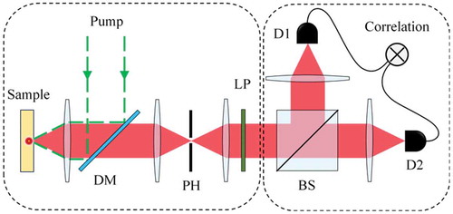
A single-photon source (SPS) refers to an optical source that can produce a specified number of photons at a specified time [Citation1]. Assuming that there is only one emitter within the small area of the excitation light focus, it will give off only one photon in an excitation-emission process. The emission collected from that spot would be single-photon sequence, that is, the photon emission of SPS is ought to be satisfied with the sub-Poisonnian statistics. The confocal microscopy (CFM) system has significantly improved the contrast and resolution of the scanning image by eliminating the noise signal from outside focal plane, such as dust fluorescence in the air, glass fluorescence from substrate or autofluorescence from optical component as shown in . The confocal microscope usually excites the emitter and collect photoluminescence with the same microscope objective to achieve bright SPS with high signal-noise ratio (SNR). To determine a SPS, hence, massive data about the correlation between the photons from the emitter should be measured. Experimentally, one often utilizes the Hanbury-Brown and Twiss (HBT) interferometer to identify a SPS. During the measurement of HBT interferometer experiment, the collect photons from the confocal microscope would be divided into two paths by a beam splitter (BS), and then be focused on the detectors, which convert the optical signals into electrical signals and typically transmit them to a time to digital converter (TDC) to measure their correlation. And the correlation measurement result is given by
where is the raw correlation events over a total measure time T and ω is the resolution of time interval,
and
are counting rates of two detectors, respectively. The antibunching evidence for a SPS appears as a dip below 0.5 in the recorded delay function around τ = 0.
Figure 1. Schematic illustration of experimental apparatus for exploring the correlation between photons. The system consists of the confocal system (left) and the HBT interferometer (right). Pump: excitation beam; DM: dichroic mirror; PH: pinhole; LP: long past filter; BS: beam splitter; D1, D2: detectors
The SPS have been demonstrated by an isolated quantum system in different configurations, such as a single atom [Citation2] or molecule [Citation3], a single quantum dot [Citation4] and a single solid-state color center [Citation5]. The focus of this review, however, is on the solid-state color centers, because it is more stable and be operated and controlled at room temperature more easily compared to other forms. In particular, the SPS based on color centers in diamond has been employed in various practical applications according to its different virtues. One prominent example is the proof of wave-particle duality of light [Citation6,Citation7]. Additionally, since color centers in the diamond are nontoxic, they are also suitable for biosensing and bioimage in a living organism [Citation8,Citation9].
For the development of a SPS platform, factors that must be considered include scalability, manufacturing process feasibility, and compatibility with existing mature processes. Although the exploration and research of new alternative solid-state material platforms of SPS, such as low-dimensional van der Waals materials and II–VI and III–V materials [Citation10,Citation11], has never been stopped, the most notably object of study at present is the SPS of point defects based on diamond, silicon carbide and boron nitride. In this review, we mainly focus on the state of the art of the SPS based on single color centers in the diamond and highlight their manufacturing processes and application areas. In theory, pure diamonds have one of the widest bandgaps (5.5 eV) of any known materials and are therefore transparent to light from the ultraviolet to the far infrared. And for that reason, there is a wide variety of impurity- and vacancy-related color centers with emission from ultraviolet to the near infrared, more than 100 of which are known in the diamond [Citation12]. Of these numerous known color centers, several photostable ones have been considered as the candidates for ideal SPSs as listed in . Among them, nitrogen vacancy (NV) center composed of a substitutional nitrogen atom with an adjacent vacancy has attracted most attention because it is easier to prepare and its fluorescence is extremely bright and stable at room temperature [Citation13,Citation14]. Besides, while the NV center was discovered and studied firstly, narrower spectral width and shorter fluorescence lifetime were found in the subsequent group IV center [Citation15–24], which are consisted of a group IV element located at the center of two vacancies. In particular, the silicon vacancy center (SiV) with an ultrashort lifetime (about 1.1 ns only) [Citation15,Citation16], which facilitates the production of high-rate single photon stream and has been utilized to develop the SiV-based quantum communication [Citation17]. And the narrow spectral width (~5 nm) of germanium center (GeV) [Citation18,Citation19] make it suitable for establishing a SPS with high SNR, which is beneficial to fabricate highly integrated quantum network [Citation20]. For most of them, the wavelengths of zero-phonon lines (ZPLs) are in the visible region except for NE8 (‘NE’ stands for nickel exhibition) center consisting of a nickel atom surrounded by four nitrogen atoms, which emits near-infrared light (793/802 nm) [Citation25,Citation26] and can be a SPS candidate for the earth-satellite quantum communication. Regarding the other color centers including zinc vacancy (SnV) [Citation22,Citation23], lead vacancy (PbV) [Citation23,Citation24] and Cr-related centers [Citation27,Citation28] reported recently, they deserve more research and attention because all of them possess several striking qualities including narrow spectral width, high brightness, and short lifetime.
Table 1. Several SPSs based on color centers in the diamond and their optical properties
Before better understanding and applying these color centers in different areas, how to use modern technology to produce these color centers more quickly and precisely is a huge challenge that cannot be avoided in the development. In the process of fabricating artificial color centers, the early technologies include annealing, ion implantation, chemical vapor deposition (CVD), and etc. In addition, new methods have emerged in recent years to realize the preparation of color centers in the diamond, such as electron bombardment and femtosecond laser irradiation. Although all of these methods offer the possibility of obtaining single color centers, none of them has yet been developed to meet all the performance requirements for potential applications.
In the following section, we will first discuss the preparation of single color centers in the diamond, including CVD, electron radiation, heavy ion radiation, ion implantation, and laser irradiation in Section 2. Then, various applications of NV centers and the other color centers in the diamond would be depicted in Section.3. Finally, in Section.4, there will be a review of this paper with a brief outlook.
2. Fabrication
Due to the remarkable performance of the NV centers in the diamond, optical color centers in the diamond are rapidly becoming one of the focus of research in solid-state quantum systems [Citation29]. The most widely accepted mechanism for the formation of color centers in the diamond is that the inner lattice vacancy would move during annealing above 600°C and then be captured by the impurity atoms in crystal to form the corresponding color centers [Citation30]. To create these vacancies, carbon atoms in the lattice can be blasted away by the irradiation of high-energy particles such as ions and electrons. When it comes to the atom source to form impurities, in addition to the impurities existing inside the diamond (the most common one is nitrogen atoms), outside atoms can also be artificially implanted and doped into diamond crystals. In the current common mature material processing technology [Citation31], it can be used to prepare diamond color centers by annealing, ion implantation, chemical vapor deposition (CVD), laser irradiation, etc. Among them, laser irradiation is a pure optical preparation method, which has been developed only in recent years, and NV color centers have been successfully prepared in the diamond by using this method. Moreover, the laser irradiation method has also been demonstrated to create single SiV color centers in diamond with outside Si atoms. Because of the advantages of simple and flexible operation, high efficiency, and high controllability at room temperature, this technology opened a new way for the development of practical and reliable preparation of single color centers in the diamond. With the development of the research on color centers in the diamond, different kinds of color centers and corresponding preparation methods has been explored to meet the special requirements of various applications, although it remains challenging for preparing single color centers with better physical properties more quickly, simply and accurately.
2.1. Chemical vapor deposition
Figure 2. Schematic diagram of microwave plasma chemical vapor deposition chamber for growing diamond. Figure redrawn according to Ref [Citation32]
![Figure 2. Schematic diagram of microwave plasma chemical vapor deposition chamber for growing diamond. Figure redrawn according to Ref [Citation32]](/cms/asset/70a99eba-e670-40f4-8617-31d2ea811c21/tapx_a_1858721_f0002_oc.jpg)
Chemical vapor deposition (CVD) technology is one of the most common methods for diamond growth [Citation33,Citation34] from carbon gas sources such as methane/hydrogen gas mixture, which is usually decomposed to form plasma in a high temperature and vacuum environment. The typical CVD cavity of microwave plasma-growing diamond is given in . Carbon-based groups are deposited and crystallized to form diamond on the substrate after complex chemical and physical reactions. The temperature of the substrate material is generally maintained at 700 °C to 900 °C [Citation35]. Noteworthy, most of the diamond materials used in industrial application are grown in this way [Citation36,Citation37]. The preparation of the diamond color center by CVD method is to mix a certain amount of impurities (such as nitrogen or silicon) in the reaction chamber of growing diamond, and form the corresponding color centers during the growth process of the diamond [Citation38,Citation39]. There are two common sources of impurities in the CVD diamond, one of which is the etching of solid substrates containing impurities by hydrogen atoms in the plasma. For example, to prepare the SiV color center in the diamond, one can choose silicon chip or quartz and other materials containing silicon as the base [Citation40]. The other one is doping by means of gas with impurity elements passing through the CVD chamber [Citation41]. Generally speaking, the use of solid doping source is conducive to the preparation of shallow color centers, which are close to the surface of one side of the base, while to better control the formation of color centers, the use of gas source doping form is required.
The preparation of diamond color centers by CVD method offers many advantages, such as the size of diamond crystal and the concentration of diamond color center can be well controlled by the growth time, the substrate selection of diamond growth is diversified, and specific impurity elements can be doped [Citation38]. This method can be used to grow bulk diamond [Citation42], diamond nanocrystals [Citation25], and diamond thin films [Citation43], where the size of the diamond crystal is a very important parameter. For example, diamond nanocrystals can effectively eliminate the reflection loss of color center fluorescence in the bulk diamond, thus enhancing the efficiency of fluorescence collection efficiency [Citation44,Citation45]. Moreover, the biocompatibility of nanodiamond combined with the stable fluorescence of NV center enables quantum sensing in living cell [Citation8,Citation46–48].
Besides silicon wafer, quartz, sapphire, and other substrates, in particular, the CVD diamond can also grow on the end face of the optical fiber [Citation49], so as to prepare optical fiber integrated diamond photonic devices with color centers. In 2005, Rabeau et al. successfully realized CVD diamond growth on the optical fiber interface, which laid a foundation for the preparation of single color centers for optical fiber integration [Citation50]. There is no doubt that the artificial diamond crystal grown by CVD can accurately eliminate the influence of unnecessary impurity elements, so as to obtain the diamond crystal with high purity, which also provides a relatively pure environment for the preparation of high-quality color centers. This is especially important for the applications of single color centers in quantum sensing. It is also worth mentioning that NV color centers prepared by this technique usually have a long coherence time, which can reach the order of milliseconds at room temperature at present [Citation51].
However, because the impurity elements doped in the crystal growth process are randomly distributed, the spatial position of single color centers cannot be arranged, nor can the depth of the color centers be well controlled. These factors, to some extent, limit the applications of the color center prepared by this method in quantum sensing. To solve this problem, the researchers combined the δ-doping technique and doped the diamond in the final stage of CVD growth to prepare the thin layer containing color center near the surface [Citation52]. Although the quality and depth of the color centers in diamond has been alleviated, there is still much room for the improvement in three-dimensional position control.
2.2. Electron irradiation
Figure 3. Concept of electron beam irradiation. The inset shows the schematic of δ-doped diamond. Figure redrawn according to Ref [Citation53,Citation57]
![Figure 3. Concept of electron beam irradiation. The inset shows the schematic of δ-doped diamond. Figure redrawn according to Ref [Citation53,Citation57]](/cms/asset/c4ae3e9a-4d68-45c4-9907-cbfd6263a812/tapx_a_1858721_f0003_oc.jpg)
The method of electron beam irradiation is mainly used in the preparation of NV color centers in the diamond which contains nitrogen naturally. The principle is to focus the electron beam on the diamond crystal by a transmission electron microscope, scanning electron microscope or other high-energy electron accelerators, as shown in . Since the electron beam bombardment effect can only produce vacancies in the diamond lattice, the irradiated diamond samples are generally rich in impurities, such as type Ib diamond [Citation54] and nitrogen ion-implanted diamond [Citation55]. Some high-energy electrons collide inelastic with carbon atoms in the diamond crystal, so that carbon atoms in the crystal lattice are driven away and a large number of lattice vacancies are formed [Citation45]. The irradiated samples need to be annealed at high temperature (higher than 600 °C), so that the newly generated lattice vacancies can move and diffuse in the crystal, and then combine with the substitutional nitrogen to form NV color centers. By adjusting the electron dose, energy and time of the bombarded electron beams, the prepared NV color center density and the depth from the surface can be controlled. High concentration of electron beam irradiation can efficiently transform a single nitrogen defect in a suitable crystal lattice into an NV color center, thus greatly increasing the production yield efficiency of NV color centers in the diamond. When compared with a commercially available high-energy irradiation process (Golan plastic), TEM irradiation has slightly higher N-NV conversion efficiency for CVD diamond, while allowing varying NV concentrations fabricated within one sample more easily [Citation56]. The stable and high-intensity luminescence characteristic of this high concentration is essential for the application of fluorescent markers [Citation8], and also helps to improve their sensitivity in magnetic field detection [Citation46].
In 2016, McLellan et al. demonstrated three-dimensional locatable NV color centers in the diamond by the combination of a transmission electron microscope and a δ-doped layer [Citation57], see the inset of . In this way, artificial vacancies can be laterally confines to less than 450 nm. A film of 4 nm-thick is formed from nitrogen δ-doping during CVD diamond growth, as shown in . Although the electron irradiation can effectively prepare a high concentration of NV color centers, this method requires diamond samples to be rich in nitrogen impurities, so it is very inappropriate to restrict the preparation of NV color center ensemble to the effective preparation of a single color center. Note that the samples need to be annealed at high temperature after irradiation, and the coherent time of these color centers can be up to millisecond.
2.3. Heavy ion irradiation
In order to create lattice vacancies efficiently, the heavy ion irradiation method can be similarly used to achieve the color center preparation. The high-energy electron beam is replaced by the high-energy heavy ion beam. As in the electron irradiation method, the diamond sample must be rich in impurities atoms, and the irradiated samples also need to undergo high-temperature annealing to effectively prepare the color centers (mainly NV). At present, the heavy ions used in the preparation of diamond color centers include lithium ion, nitrogen ion, carbon ion, gallium ion etc. In the early studies, such as Ref [Citation58]., Martin et al. used a 30 KeV focused gallium ion beam to irradiate type Ib diamonds which are rich in nitrogen impurities. Subsequently, samples were annealed in a vacuum for 1 h at a high temperature above 750°C to achieve the preparation of NV color center arrays with transverse space control. Although the resolution of the prepared color center array in the transverse space were less than 180 nm, the distance between the NV color centers and the surface could not be accurately controlled due to the large energy of heavy ions. In 2014, Ohno et al. controlled the depth of the color center precisely by combining nitrogen-doped diamond and 12C ion irradiation technology [Citation59]. Meanwhile, by further combining with the diamond surface microporous template, the position of the color center can be accurately controlled in three dimensions. It was reported that an individual NV center can be prepared within a volume of (~180 nm)3 at a deterministic position while repeatedly preserving a long coherence time (T2 > 0.3 ms) [Citation59]. It enables integration into NV-based nanostructures by this deterministic position control of coherent NV centers. Therefore, scalable spin-sensing devices may become true as well as coherent spin coupling mediated by photons and phonons.
The technique of producing NV color centers by heavy ion irradiation [Citation60] also has potential applications in fluorescence nuclear track detectors [Citation61]. Although this preparation method can effectively and accurately prepare NV color center in three-dimensional space, or even a single color center, the heavy ions radiated into the crystal will stay in the crystal lattice. Besides, high ion concentration will cause great damage to the crystal structure of the diamond, thus affecting the performance of the formed color center [Citation62].
2.4. Ion implantation
Figure 4. (a) Schematic diagram of ion implantation according to Ref [Citation64].; (b) Fluorescence image of the silicon-implanted region on the diamond sample after annealing; (c) Fluorescence scan image of a single SiV color center, the inset is fluorescence photon correlation measurement of this color center; (d) Line-scan across the SiV center along Y-axis and a fit with Gauss function
![Figure 4. (a) Schematic diagram of ion implantation according to Ref [Citation64].; (b) Fluorescence image of the silicon-implanted region on the diamond sample after annealing; (c) Fluorescence scan image of a single SiV color center, the inset is fluorescence photon correlation measurement of this color center; (d) Line-scan across the SiV center along Y-axis and a fit with Gauss function](/cms/asset/a245015c-5642-4594-9a8d-5e1ee1093e99/tapx_a_1858721_f0004_oc.jpg)
Similar to the electron and the heavy ion irradiation methods, the ion implantation also uses high-energy particles accelerated by electric fields to shock and replace in-situ atoms in the crystal lattice [Citation63,Citation64], as shown in ). The depth of the ions injected by ion implantation depends on the mass and energy of the accelerated ions (generally ranging from a few keV to MeV). In 2019, Raatz et al. proposed a novel nano-implantation technique, in which low-energy (< 10 keV) ion implantation is combined with a pierced atomic force microscope (AFM) tip used as a nano-aperture to collimate the ion beam down to nanometer size [Citation65]. The result shows that ion scattering at the aperture and the ion channeling effect can be effectively inhibited by optimizing the parameter of tip and the surface roughness, resulting in further improvement of the resolution in implanting single ions in the diamond. Damage to diamond crystals and high-temperature annealing in the later stage are also inevitable. The difference here is that the accelerated ions are the impurity elements corresponding to the color centers to be prepared. ) shows the fluorescence image of the diamond samples of SiV color centers prepared by ion implantation method provided by Waseda University [Citation66]. The divalent silicon ions are first implanted into the diamond at an accelerated energy of 60 keV, and the sample is then annealed for half an hour at 1000 °C in a synthetic gas atmosphere containing 10% hydrogen. ) shows a confocal microscope scanning imaging of a single SiV color center of this sample. ) shows line-scan across the SiV center along Y-axis and a fit with Gauss function. The FWHM of a single fluorescent spot is about 300 nm which is close to the diffraction limit of the confocal microscope.
During the implantation process, the number of ions into the sample can be controlled by the ion beam current and irradiation time. In ion implantation technology, one can select different external impurities [Citation28] (such as nitrogen ion, silicon ion, etc.) to inject into the diamond to prepare different types of single color centers, which has higher flexibility. Its advantage lies in its ability to accurately control the three dimensions in space of the ion implantation crystal, so the color center prepared has a high controllability in three-dimensional distribution, and the spatial resolution can reach several nanometers. The single color centers prepared by this method are of great importance in the application of quantum information and quantum sensing. As known that the depth of the color centers in diamond is an important factor in the ultra-sensitive quantum sensing. The closer the prepared color center is to the diamond surface, the more sensitive it feels to the changes with the external environment, thus the higher the detection sensitivity will be. As the depth of single color centers prepared by ion implantation increases with the increase of the ion energy, ultra-shallow single NV color centers can be prepared, which is also the main preparation method for SPS used as a quantum sensor [Citation66].
More and more single color centers with different atom impurities have been prepared in the diamond by this method, like lead-related single color centers [Citation24] and single SnV color centers [Citation67]. Besides, entanglement between NV pairs [Citation68] and strongly coupled triple NV centers [Citation69] were achieved by ion implantation, which can be further extended to prepare integrated quantum devices by combining high-resolution ion implantation [Citation64].
2.5. Laser irradiation
Figure 5. (a) Fs laser was focused on the diamond sample surface. (b) Schematic drawing of plasma waveguide approximated according to Ref [Citation74]. (c) Fluorescence scanning images of three spots after 1/125 s fs pulse laser illumination and 15-minute oxidation. (d) Typical fluorescence spectrum of the illuminated spots, showing clearly zero-phonon line at 637 nm
![Figure 5. (a) Fs laser was focused on the diamond sample surface. (b) Schematic drawing of plasma waveguide approximated according to Ref [Citation74]. (c) Fluorescence scanning images of three spots after 1/125 s fs pulse laser illumination and 15-minute oxidation. (d) Typical fluorescence spectrum of the illuminated spots, showing clearly zero-phonon line at 637 nm](/cms/asset/baaf3c4d-2a2b-44b7-9378-ee19b221e5c1/tapx_a_1858721_f0005_oc.jpg)
In recent years, fs laser technology has been developed to easily and flexibly fabricate single NV color centers with excellent optical properties. As early as in 2004, Dumeige et al. had transformed the negative charged NV color center into a neutral NV color center by the excitation of focused fs laser [Citation70]. During the irradiation, the fluorescence intensity first increased and then decreased, and the final intensity became more than twice that of the initial single color center in nano-diamond which was fabricated by the electron irradiation. In 2013, Liu et al. had fabricated single, multiple, and large-area high-density ensembles of NV color centers in the synthetic Type Ib bulk diamond by focusing the near-infrared fs laser in the area about 1–2 μm above the diamond sample, as shown in [Citation71]. This method is the same as the electron irradiation in the formation of the lattice vacancies in crystal, but the high-energy electron beam is formed by the fs laser filament effect in the air. In the region of fs laser filamentation [Citation72,Citation73], the molecules in the air (oxygen, nitrogen, etc.) will be ionized by the strong electromagnetic field and high-energy electrons [Citation74,Citation75] (see )). During the fs laser irradiation, high-density plasma bombards diamond crystals to create lattice vacancies [Citation76]. Typical photoluminescence (PL) spectra of NV centers could be observed on the illuminated spots after high-temperature annealing, in ). By controlling the duration of time of fs laser irradiation, the density of NV color center generated can be controlled. Meanwhile, the diamond crystal in the irradiated area is damaged greatly, and even graphitization occurs in the irradiated area. In recent years, Chen et al. used a high-aperture oil-immersion microscope (N.A. = 1.4) to focus the fs laser, so as to obtain a smaller irradiation area [Citation77]. At the same time, combined with the spatial light modulator, the aberration in the experiment has been corrected appropriately to reduce the divergence of the fsd laser-focused inside the diamond crystal. The concentration of the energy also enhances the interaction between the fs laser and the diamond. The real-time preparation and detection of the single color centers can be carried out at the same time, which greatly simplifies the process and conditions of preparation. This method can achieve the precise positioning of array of single NV color center in diamond, and its spatial resolution accuracy reaches 33 nm [Citation78]. However, these accurately prepared individual color centers are far away from the crystal surface (> 10 μm) [Citation79], which limits the sensitivity of magnetic field and temperature measurements [Citation80].
In addition to the preparation of single NV color centers with high quality and precision based on mature micro-nano processing technology, in 2017, fs laser was used to prepare a three-dimensional optical waveguide inside the diamond that could be used for the fluorescence transmission of NV color centers which could be created under the same conditions as the waveguide [Citation81]. This provides a basis for the integration of the two outcomes. In the following year, Hadden et al. realized the coupling between a single NV color center and a single-mode optical waveguide in diamond in the similar way [Citation82]. Because of the enhancement effect of waveguides and the long-distance quantum entanglement property, the integrated single NV color center has a promising application prospect in the nanoscale ultrasensitive quantum sensing and quantum computation.
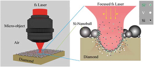
Figure 6. (a) A diagram of fs laser-focused on diamond coated with silicon nanoball; (b) The formation mechanism of SiV color center. Figure redrawn according to Ref [Citation83]
![Figure 6. (a) A diagram of fs laser-focused on diamond coated with silicon nanoball; (b) The formation mechanism of SiV color center. Figure redrawn according to Ref [Citation83]](/cms/asset/e9f4ea84-4ac1-4c51-95dd-cfcc2bd4cefc/tapx_a_1858721_f0006_oc.jpg)
Figure 7. (a) Fluorescence scanning image of fs laser irradiation area after annealing; (b) A confocal scanning imaging of a single SiV− color center in (a); Fluorescence photon correlation measurement (c) and fluorescence spectra (d) of the single SiV− center in (b)
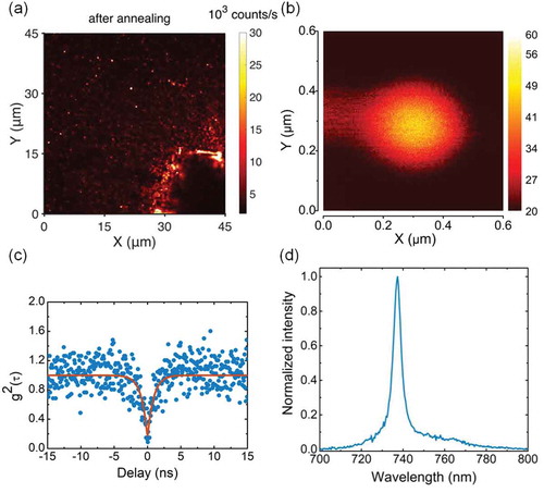
In 2019, Rong et al achieved the preparation of single negatively charged silicon vacancy (SiV−) color centers by focusing fs laser on top of a high-purity diamond coated with a layer of Si nanoballs (see )) [Citation83]. As to insulators, the Coulomb explosion is a basic process of high energy fs laser irradiation that causes the avalanche ionization of Si nanoballs [Citation84]. The fs laser fluence was about 1.6 J/cm2, which was high enough to spark the Coulomb explosion [Citation85] which gave rise to the fast ejection of positive ions (see )). After one hour’s annealing at 850°C in vacuum, the PL scan image of bright spots around the created crater was shown in ), where a single SiV− center was found ()), which can be proved by the results of second-order autocorrelation measurement and PL spectra shown in ) respectively. Compared to the methods above, this method is convenient and time-saving to generate SiV centers in diamond. In addition to SiV color centers, it’s interesting that a large number of NV color centers can be observed in the area irradiated by fs laser even before annealing in our experiment [Citation86]. This indicates that a layer of Si nanoball coated on the diamond surface has the effect of annealing in the forming process of NV color centers.
To sum up, it is feasible to prepare the color center in diamond at ambient environment with all-optical technology such as fs laser writing process. When the multi-photon ionization process is introduced to prepare the vacancies in diamond, the vacancies can be precisely located in the desired region focusing the femtosecond laser with a high numerical aperture (NA = 1.4) microscope objective with aberration correction [Citation77]. However, the conventional annealing process will make the diffusion of the holes uncontrollable (~ 200 nm), resulting in the failure of locating the NV color centers within the desired region. As the samples in the annealing process cannot be observed online, the success rate can only be estimated from the final product. By femtosecond laser local annealing, which uses femtosecond pulses with lower energy to irradiate the same region, the generation of fluorescent color centers can be monitored in real time, and the spatial resolution of color centers can be greatly improved [Citation78]. Different from the direct interaction of the photon and the lattice, femtosecond laser with the high-energy flow density (> 0.8 J/cm2) will ionize the molecules in the air and creating a plasma channel, in which high-energy electron beams can be generated. These high-energy electrons can blast the crystal lattice of diamond to generate a large number of lattice vacancies, but the conventional annealing process is still required to make these vacancies move to form the NV color centers. And a large number of NV color centers can be directly produced in a diamond-coated with silicon nano-ball in the area of the plasma channel created by femtosecond laser without annealing [Citation86]. Here, it is worth noting that coulomb explosion effect caused by the femtosecond laser interaction with silicon nano-ball not only can implant a doped silicon ions into diamond lattice, but also contributes to the diffusion of the vacancies. Further annealing process is needed to form a stable SiV color center [Citation83]. At present, the coherent time of a single NV color center prepared by the femtosecond laser illumination can reach more than 100 μs [Citation77] which is comparable to those prepared by the ion electron irradiation [Citation56] so that this method could be a new path for the preparation of single-photon source to be applied in quantum technologies.
3. Applications of color centers in the diamond
Nowadays, imposed by the quantum mechanics, most modern devices, however, are reaching their limitations, which have driven the research and development of quantum technology to make breakthrough in metrology, information processing, and imaging resolution. To this end, the color centers in the diamond, especially the NV center, is considered to be a promise material for its outstanding optical and spin properties. Besides, due to their low cytotoxicity, the diamond-based systems are prominent candidates for biomedical research like biosensing. More recently, as described in the previous sections, the manufacturing process of color centers has gradually matured, which is also a huge motivation for developing the applications of color centers in diamond. In this section, current and future applications of NV centers (Section 3.1~3.4) and others (Section 3.5) in these areas will be discussed.
3.1. Metrology
With respect to metrology, most studies are aimed at gaining a higher accuracy in the process of measuring a physical quantity. As a single electronic spin defects in diamond, NV center can be initialized and readout optically under ambient condition, and its energy levels are highly sensitive to changes in external factors such as magnetic field, electrical field, temperature, pressure. Hence, it offers new opportunities to achieve nanoscale measurement at a much lower cost than other quantum sensors like superconducting quantum interference devices (SQUID) [Citation87,Citation88], atomic vapor [Citation89], trapped ion [Citation90], which require extreme experimental environment.
Figure 8. Electronic structure of NV center in diamond
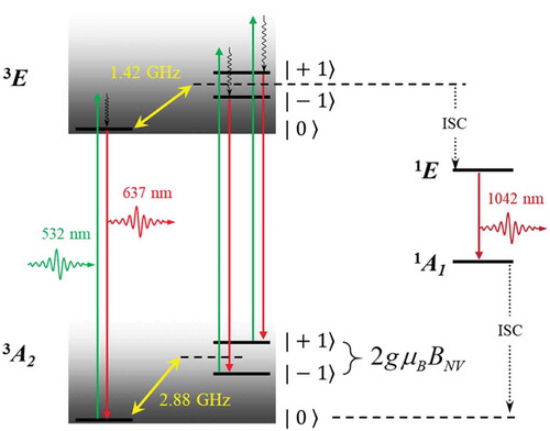
The idea of applying NV centers to detect the magnetic field was first proposed a decade ago [Citation91,Citation92]. The ground state of NV center is a spin triplet level 3A2 composed of ms = 0, ±1 sub-levels, and it can be optically excited to its excited state 3E, which is also a spin triplet level, as shown in . The spin property of this defect is conserved during this transition and its PL intensity is spin-dependent, where ms = 0 state shows a significantly brighter luminescence than ms = ±1 state. It would cause a resonance absorption driving ms = 0 state to ms = ±1 state at zero external magnetic field, when a microwave (MW) of about 2.87 GHz is applied, resulting in a dip in the PL spectra called optically detected magnetic-resonance (ODMR) spectrum. Moreover, the ms = ±1 sub-levels are second split in a bias magnetic field near NV center due to the Zeeman effect, hence two and more resonance lines would appear in the ODMR spectrum.
Based on the ODMR technology, NV-based magnetometer has achieved broad bandwidth (up to 100 kHz) [Citation93], high frequency (GHz) [Citation94,Citation95] and high sensitivity (~ pT/√Hz) [Citation46] magnetic field detection, and it has the capacity to determine the direction of an arbitrary static magnetic field in three-dimensional space [Citation96]. All of the above advantages stimulated numerous applications about NV-based magnetometer, including the studies of cytology [Citation97,Citation98], meteoritics [Citation99], paleomagnetism [Citation100,Citation101]. In particular, such a magnetometer was used to detect and analyze the protein [Citation102] which is the material basis of life. Additionally, this method has also been exploited in the magnetic detection of single-neuron action potentials from both single neuron and intact marine worms without any adverse reactions [Citation103], which is advantageous for studying the structure and phenomena of the nervous system in more complex organisms. Recently, NV-based magnetometry has been also applied in the research field of high-pressure physics [Citation104–106] by using implanted NV ensemble on the surface of a diamond anvil culet or by using NV-contained diamond particles in the high-pressure chamber. By attaching ubiquitin proteins to the diamond surface and using a proximal NV center as quantum sensor, Lovchinsky et al. showed NMR detection and spectroscopy of individual proteins [Citation107], where the magnetic field sensitivity was enhanced by improving the readout fidelity and coherence properties of NV center, which were realized by a quantum logic and a surface-treatment, respectively.
The NV center is also used as the nanoscale sensor of pressure and temperature, because a change of an external factor would generate the strain in the diamond crystal and induce the lattice distortion, which shifts the resonate peak in the ODMR spectrum. Experimentally, a temperature sensitivity of 76 μK/√Hz [Citation47] and a pressure resolution of 0.6 MPa/√Hz [Citation48] were achieved in the terms of NV-based thermometer and manometer, respectively. In the field of thermometry, this kind of thermometer has been applied in the living cell [Citation108] on the basis of the non-invasive peculiarity to organisms as we described above, which encouraged the study about thermogenesis to learn more about biological mechanisms.
3.2 Quantum information
Contemporarily, quantum information technology composed of quantum computing and quantum communication has attracted worldwide attention due to its potential to open up a new generation about information processing. Not only could this revolutionary technology dramatically improve the power of information processing, but also it would settle the problem of quantum communication as well. Particularly, it has been demonstrated that the NV center in the diamond is a promising implementation of this technique for its long-spin coherent time and well-defined optical transitions at room temperature.
3.2.1. Quantum computing
Classical information is a string of binary digit, whose unit is called bit that either exists as 0 or 1, whereas they could exist simultaneously for a quantum bit (qubit), the unit of quantum information. Based on the qubits, quantum computing could advance the storage capacity and processing speed for information dramatically. Thus, it is possible to enhance the performance of computer sequentially by quantum computing. While qubit can be achieved by many ways, NV center is an outstanding one and has been investigated widely since the realization of two-qubit conditional quantum gate (CROT) [Citation109]. Recent progresses of quantum computing applications performed by NV center include quantum register [Citation110], quantum error correction (QEC) [Citation111,Citation112], two-qubit gate [Citation113], and quantum algorithm implementation based on both Deutsch-Jozsa algorithm [Citation114] and Grover search algorithms [Citation115]. In particular, Waldherr et al. demonstrated three-qubit phase-flip error correction in a diamond spin system with high-fidelity operations including joint initialization, projective readout and fast local and non-local gate operations [Citation112], which were all close to the required fidelities for fault-tolerant quantum operations. In Ref [Citation113]., Rong et al. designed an optimal control method for the NV-based CNOT gate and achieved a two-qubit gate with highest fidelity (0.992) in solid-state spin system. Besides, a two-qubit solid-state quantum processor with the competence of implementing arbitrary unitary operation was performed through electron spin and 14N nuclear spin of NV centers in the diamond [Citation116]. And there are massive other works on this topic we will not discuss due to the article length limitation, but it is optimistic about the future of quantum computer according to the development trend in recent years.
3.2.2. Quantum communication
As a good SPS, the NV center has been used to realize quantum communication by QKD [Citation117]. The first implementation was reported in 2002, Beveratos et al. used NV center to generate single photon sequence and achieved a 50 m-long QKD in a corridor with a secure bit rate of 7700 s−1 [Citation118]. After that, Alléaume et al. demonstrated a new NV-based QKD system worked between two buildings, which promoted the feasibility of this technology working in free space and brought it closer to reality [Citation119]. More recently, a study of great significance achieved 3-meters-long entanglement by two separate NV center in 2013 [Citation120], and this distance extended to 1.3 km two years later [Citation121]. Furthermore, due to the ability of spin-photon entanglement, a loophole-free Bell inequality test [Citation121], entanglement distillation [Citation122], and deterministic entanglement [Citation123] have been demonstrated, as one of the most exciting signs of progress in the field of quantum information. Moreover, single-memory [Citation124] and so-called single-photon [Citation125] scheme was proposed to establish the quantum repeater required for quantum communication at greater distance in 2017 and 2019, respectively.
3.3. Super-resolution imaging
Super-resolution optical microscopy is the most representative technique in the context of optical microscopy this century for its breakthrough of optical diffraction limit. One prominent invention is stimulated emission depletion (STED) microscopy proposed by Hell and his coworkers in 1994 [Citation126], where two strictly coaxial lasers was required in typical example, one to excite the sample to produce the fluorescence, and the other, a doughnut-shaped laser, to excite the sample at the edge of the excited light, thus limiting the fluorescence emission to a small area in the middle and resulting in a fluorescent spot smaller than diffraction limit. Due to its exquisite photostability, the NV centers are ideal to achieve the highest possible spatial resolution with STED [Citation127], and it has been demonstrated a striking resolution of 6 nm by detecting single NV center in diamond with STED microscopy in 2009 [Citation128]. Moreover, by manipulating the charge state of NV center, another subdiffractional resolution of approximately 4 nm imaging technique was achieved at a lower laser power [Citation129], which is called charge-state depletion (CSD) microscopy. Compared to STED, using the lower power laser makes CSD to produce less photodamage that would be helpful for super-resolution imaging in a biological system. Other implementations including ground state depletion (GSD) microscopy [Citation130], deterministic emitter switch microscopy (DESM) [Citation131], single-spin stochastic optical reconstruction microscopy (STORM) [Citation132] has also been reported.
3.4. Biological applications
As mentioned before, one prime advantage of NV center in diamond is good biocompatibility, which has aroused great interest and extensive research on the aspects of biological application. In 2007, fluorescent nano-diamonds (FND) with both NV0 and NV− was used to be a biomarker in a HeLa cell. During the continuous excitation of sample up to 20 minutes [Citation8], bright and stable fluorescence signal was observed, and it turns out FND can be utilized for long-term tracking in cell. Furthermore, combined with the aforementioned nano-sensor and super-resolution imaging technology, applications of NV centers in biosensors [Citation9] and bioimaging [Citation97,Citation133] have also been demonstrated respectively. In particular, Hall et al. achieved wide field imaging of planar neuron by means of NV-based ODMR technique to investigate the activity of neuronal network, reaching simultaneously high temporal and spatial resolution, which is a significant work for understanding the information processing mechanism in our brain [Citation134].
3.5. Applications on other color centers
Except NV centers, other color centers in diamond has also shown great potential in various fields although it’s still in its infancy. Above all, the group-IV defects are more suitable than NV center in terms of quantum network, because it has more symmetrical structure, longer coherence time, less spectral diffusion at cryogenic temperature, and narrower inhomogeneous broadening. For example, Liu et al. investigated the PL properties of a single SiV center in 2015 [Citation17], where a triggered SPS for high-speed QKD was achieved under the excitation of ultrafast laser with high pulse repetition frequency. Besides, by coupling the SiV centers to the nano-cavities, quantum-optical switch, tunable SPS and quantum entanglement were all demonstrated [Citation135]. Although these works were all performed in a cryogenic environment, they bring the scalable quantum networks closer to reality. More recently, SiV center was also utilized to polarize nuclear spins determinately via Hartmann–Hahn double resonance [Citation136], which offered a hybrid method for initialization and readout of nuclear memory. In addition, it was proposed that electrically driven luminescence can be achieved by group-IV defects unlike NV center where the luminescence is driven optically. In these years, several successful cases of SiV-based electroluminescence (EL) have been reported actually [Citation137,Citation138]. In particular, Bray et al. used single crystal diamond contained SiV center as i-layer and demonstrated a nanoscale diamond-diode with good PL and EL characteristics [Citation139]. The same year, Hamidreza et al. designed and fabricated a dielectric-loaded surface plasmon polariton waveguides embedded a single GeV center to realize remote-control excitation and fluorescence collection of GeV center in a plasmonic chip, and an approximate 6-fold Purcell enhancement compared to the emission in the case of uncoupled GeV was also observed [Citation20]. The other centers in diamond, however, were also proved good performance in the context of quantum sensing that is identical in the case of NV center, and recent example of sensing temperature was achieved via SiV [Citation140], GeV [Citation141], and NE8 [Citation142].
4. Summary and outlook
Overall, a concise description and recent progress of color centers in diamond are illustrated in this review, and it’s obvious that the interest of color centers in diamond has remained intensive over the few past decades. In preparation, while typical methods like CVD have matured and been exploited to prepare kinds of color center in diamond, the advent of laser writing technology, a novel and full of vitality micromachining technology, has improved both the speed and precision of fabrication process, and greatly increased the efficiency of preparing a single NV color center by combining the annealing technology and the real-time fluorescence feedback [Citation78]. This, in turn, would boost the development of NV center in practical applications, particularly the quantum network required high integration. Quantum sensing, however, remains the most promising application due to the fragile energy level that offers exceptional sensitivities to external factors, with excellent achievements in detecting magnetic field [Citation95], temperature [Citation47], pressure [Citation48] and other physical quantity [Citation143,Citation144]. Moreover, the biological harmless property of diamond renders the NV center valuable in biological applications. With regard to other color centers in diamond, although they are still in their infancy, great potential has been demonstrated in many fields, and the successful generation of SiV center by ingeniously coating the diamond surface with a layer of silicon nano-spheres subsequently illuminated by fs laser opened up an advanced idea to fabricate other color centers [Citation83]. On this basis, we can envision that more applications related to diamond color centers would be discovered with further research and understanding.
Acknowledgments
We thank Syuto Tamura, Prof. Takashi Tanii, Dr. Tokuyuki Teraji, Dr. Shinobu Onoda, Dr. Takeshi Ohshima, Prof. Junichi Isoya and Dr. Takahiro Shinada for Si-implanted diamond sample. We thank Dr Yan Liu and Dr Youying Rong for the fs irradiated diamond samples.
Disclosure statement
No potential conflict of interest was reported by the authors.
Correction Statement
This article has been republished with minor changes. These changes do not impact the academic content of the article.
Additional information
Funding
References
- Lodahl P, Mahmoodian S, Stobbe S. Interfacing single photons and single quantum dots with photonic nanostructures. Rev Mod Phys. 2015;87:347–29.
- Kuhn A, Hennrich M, Rempe G. Deterministic single-photon source for distributed quantum networking. Phys Rev Lett. 2002;89:067901.
- Lounis B, Moerner WE. Single photons on demand from a single molecule at room temperature. Nature. 2000;407:491–493.
- Santori C, Fattal D, VučKović J, et al. Indistinguishable photons from a single-photon device. Nature. 2002;419:594–597.
- Kurtsiefer C, Mayer S, Zarda P, et al. Stable solid-state source of single photons. Phys Rev Lett. 2002;85:290–293.
- Englert BG. Fringe visibility and which-way information: an inequality. Phys Rev Lett. 1996;77:2154–2157.
- Jacques V, Wu E, Grosshans F, et al. Experimental realization of wheeler’s delayed-choice gedanken experiment. Science. 2007;315:966–968.
- Fu -C-C, Lee H-Y, Chen K, et al. Characterization and application of single fluorescent nanodiamonds as cellular biomarkers. Proc Natl Acad Sci. 2007;104:727–732.
- Ermakova A, Pramanik G, Cai J-M, et al. Detection of a few metallo-protein molecules using color centers in nanodiamonds. Nano Lett. 2013;13:3305–3309.
- Tran TT, Bray K, Ford MJ, et al. Quantum emission from hexagonal boron nitride monolayers. Nat Nanotech. 2016;11:37–41.
- Morfa AJ, Gibson BC, Karg M, et al. Single-photon emission and quantum characterization of zinc oxide defects. Nano Lett. 2012;12:949–954.
- Jelezko F, Wrachtrup J. Single defect centres in diamond: A review. Phys Status Solidi A. 2006;203:3207–3225.
- Collins AT, Thomaz MF, Jorge MIB. Luminescence decay time of the 1.945 eV center in type IB diamond. J Phys C Solid State Phys. 1983;16:2177–2181.
- Beveratos A, Kuhn S, Brouri R, et al. Room temperature stable single-photon source. Eur Phys J D. 2002;18:191–196.
- Neu E, Steinmetz D, Riedrich-Moeller J, et al. Single photon emission from silicon-vacancy centres in CVD-nano-diamonds on iridium. New J Phys. 2011;13:025012.
- Rong Y, Ma J, Chen L, et al. Excited-state lifetime measurement of silicon vacancy centers in diamond by single-photon frequency upconversion. Laser Phys. 2018;28:055401.
- Liu Y, Siyushev P, Rong Y, et al. Investigation of the silicon vacancy color center for quantum key distribution. Opt Express. 2015;23:32961–32967.
- Palyanov YN, Kupriyanov IN, Borzdov YM, et al. Germanium: a new catalyst for diamond synthesis and a new optically active impurity in diamond. Sci Rep. 2015;5:14789.
- Iwasaki T, Ishibashi F, Miyamoto Y, et al. Germanium-vacancy single color centers in diamond. Sci Rep. 2015;5:12882.
- Siampour H, Kumar S, Davydov VA, et al. On-chip excitation of single germanium vacancies in nanodiamonds embedded in plasmonic waveguides. Light Sci Appl. 2018;7:61.
- Iwasaki T, Miyamoto Y, Taniguchi T, et al. Tin-vacancy quantum emitters in diamond. Phys Rev Lett. 2017;119:253601.
- Ditalia Tchernij S, Herzig T, Forneris J, et al. Single-photon-emitting optical centers in diamond fabricated upon Sn implantation. ACS Photonics. 2017;4:2580–2586.
- Ditalia Tchernij S, Lühmann T, Herzig T, et al. Single-photon emitters in lead-implanted single-crystal diamond. ACS Photonics. 2018;5:4864–4871.
- Trusheim ME, Wan NH, Chen KC, et al. Lead-related quantum emitters in diamond. Phys Rev B. 2019;99:075430.
- Gaebel T, Popa I, Gruber A, et al. Stable single-photon source in the near infrared. New J Phys. 2004;6:98–104.
- Wu E, Rabeau JR, Roger G, et al. Room temperature triggered single-photon source in the near infrared. New J Phys. 2007;9:434.
- Aharonovich I, Castelletto S, Simpson DA, et al. Two-level ultrabright single photon emission from diamond nanocrystals. Nano Lett. 2009;9:3191–3195.
- Aharonovich I, Castelletto S, Simpson DA, et al. Chromium single-photon emitters in diamond fabricated by ion implantation. Phys Rev B. 2010;81:121201(R).
- Pfaff W, Hensen BJ, Bernien H, et al. Unconditional quantum teleportation between distant solid-state quantum bits. Science. 2014;345:532–535.
- Zaitsev AM. Optical properties of diamond: a data handbook. Berlin Heidelberg: Springer-Verlag; 2001.
- Orwa JO, Greentree AD, Aharonovich I, et al. Fabrication of single optical centres in diamond—a review. J Lumin. 2010;130:1646–1654.
- Eaton-Magaña S, Shigley JE. Observations on CVD-grown synthetic diamonds: A review. Gems Gemol. 2016;52:222–245.
- Shareef IA, Rubloff GW, Anderle M, et al. Subatmospheric chemical vapor deposition ozone/TEOS process for SiO2 trench filling. J Vac Sci Technol B. 1995;13:1888–1892.
- Iakoubovskii K, Collins AT. Alignment of Ni- and Co-related centres during the growth of high-pressure–high-temperature diamond. J Phys Condens Matter. 2004;16:6897–6906.
- Iakoubovskii K, Kiflawi I, Johnston K, et al. Annealing of vacancies and interstitials in diamond. Physica B. 2003;340–342:67–75.
- Field JE. The properties of diamond. London: Academic Press; 1979.
- Collins AT, Connor A, Ly C-H, et al. High-temperature annealing of optical centers in type-I diamond. J Appl Phys. 2005;97:083517.
- Aharonovich I, Castelletto S, Simpson DA, et al. Diamond-based single-photon emitters. Rep Prog Phys. 2011;74:076501.
- Neu E, Steinmetz D, Riedrich-Möller J, et al. Single photon emission from silicon-vacancy colour centres in chemical vapour deposition nano-diamonds on iridium. New J Phys. 2011;13:025012.
- Dragounová K, Ižák T, Alexander K, et al. Influence of substrate material on spectral properties and thermal quenching of photoluminescence of silicon vacancy colour centres in diamond thin films. J Electr Eng Technol. 2017;68:3–9.
- Bolshakov A, Ralchenko V, Sedov V, et al. Photoluminescence of SiV centers in single crystal CVD diamond in situ doped with Si from silane. Phys Status Solidi A. 2015;212:2525–2532.
- Trusheim ME, Li L, Laraoui A, et al. Scalable fabrication of high purity diamond nanocrystals with long-spin-coherence nitrogen vacancy centers. Nano Lett. 2014;14:32–36.
- Ohashi K, Rosskopf T, Watanabe H, et al. Negatively charged nitrogen-vacancy centers in a 5 nm thin 12C diamond film. Nano Lett. 2013;13:4733–4738.
- Beveratos A, Brouri R, Gacoin T, et al. Nonclassical radiation from diamond nanocrystals. Phys Rev A. 2001;64:061802.
- Gruber A, Dräbenstedt A, Tietz C, et al. Scanning confocal optical microscopy and magnetic resonance on single defect centers. Science. 1997;276:2012–2014.
- Wolf T, Neumann P, Nakamura K, et al. Subpicotesla diamond magnetometry. Phys Rev X. 2015;5:041001.
- Liu CF, Leong WH, Xia K, et al. Ultra-sensitive hybrid diamond nanothermometer. Natl Sci Rev. arXiv:1912.12097. 2019.https://doi.org/10.1093/nsr/nwaa194.
- Doherty MW, Struzhkin VV, Simpson DA, et al. Electronic properties and metrology applications of the diamond NV− center under pressure. Phys Rev Lett. 2014;112:047601.
- May PW, Rego CA, Ashfold MNR, et al. CVD diamond-coated fibres. Diam Relat Mater. 1995;4:794–797.
- Rabeau JR, Huntington ST, Greentree AD, et al. Diamond chemical-vapor deposition on optical fibers for fluorescence waveguiding. Appl Phys Lett. 2005;86:134104.
- Balasubramanian G, Neumann P, Twitchen D, et al. Ultralong spin coherence time in isotopically engineered diamond. Nat Mater. 2009;8:383–387.
- Ohno K, Heremans FJ, Bassett LC, et al. Engineering shallow spins in diamond with nitrogen delta-doping. Appl Phys Lett. 2012;101:082413.
- Herzig T, Racke P, Raatz N, et al. Creation of quantum centers in silicon using spatial selective ion implantation of high lateral resolution. 22nd International Conference on Ion Implantation Technology (IIT), Würzburg, Germany; 2018.
- Collins AT, Dahwich A. The production of vacancies in type Ib diamond. J Phys Condens Matter. 2003;15:L591–L596.
- Kalish R, Uzan-Saguy C, Philosoph B, et al. Nitrogen doping of diamond by ion implantation. Diam Relat Mater. 1997;6:516–520.
- Farfurnik D, Alfasi N, Masis S, et al. Enhanced concentrations of nitrogen-vacancy centers in diamond through TEM irradiation. Appl Phys Lett. 2017;111:123101.
- McLellan CA, Myers BA, Kraemer S, et al. Patterned formation of highly coherent nitrogen-vacancy centers using a focused electron irradiation technique. Nano Lett. 2016;16:2450–2454.
- Martin J, Wannemacher R, Teichert J, et al. Generation and detection of fluorescent color centers in diamond with submicron resolution. Appl Phys Lett. 1999;75:3096–3098.
- Ohno K, Joseph Heremans F, de Las Casas F, et al. Three-dimensional localization of spins in diamond using 12C implantation. Appl Phys Lett. 2014;105:383.
- Sotoma S, Yoshinari Y, Igarashi R, et al. Effective production of fluorescent nanodiamonds containing negatively-charged nitrogen-vacancy centers by ion irradiation. Diam Relat Mater. 2014;49:33–38.
- Onoda S, Haruyama M, Teraji T, et al. New application of NV centers in CVD diamonds as a fluorescent nuclear track detector. Phys Status Solidi A. 2016;212:2641–2644.
- Nagl A, Hemelaar SR, Schirhagl R. Improving surface and defect center chemistry of fluorescent nanodiamonds for imaging purposes—a review. Anal Bioanal Chem. 2015;407:7521–7536.
- Evans RE, Sipahigil A, Sukachev DD, et al. Narrow-linewidth homogeneous optical emitters in diamond nanostructures via silicon ion implantation. Phys Rev A. 2016;5:044010.
- Tamura S, Koike G, Komatsubara A, et al. Array of bright silicon-vacancy centers in diamond fabricated by low-energy focused ion beam implantation. Appl Phys Express. 2014;7:115201.
- Raatz N, Scheuner C, Pezzagna S, et al. Investigation of Ion channeling and scattering for single-Ion implantation with high spatial resolution. Phys Status Solidi A. 2019;216:1900528.
- Sutera D, Jelezkob F. Single-spin magnetic resonance in the nitrogen-vacancy center of diamond. Prog Nucl Magn Reson Spectrosc. 2017;98–99:50–62.
- Trusheim ME, Pingault B, Wan NH, et al. Transform-limited photons from a coherent tin-vacancy spin in diamond. Phys Rev Lett. 2020;124:023602.
- Dolde F, Jakobi I, Naydenov B, et al. Room-temperature entanglement between single defect spins in diamond. Nat Phys. 2013;9:139–143.
- Haruyama M, Onoda S, Higuchi T, et al. Triple nitrogen-vacancy centre fabrication by C5N4Hn ion implantation. Nat Commun. 2019;10:2664.
- Dumeige Y, Treussart F, Alléaume R, et al. Photo-induced creation of nitrogen-related color centers in diamond nanocrystals under femtosecond illumination. J Lumin. 2004;109:61–67.
- Liu Y, Chen G, Song M, et al. Fabrication of nitrogen vacancy color centers by femtosecond pulse laser illumination. Opt Express. 2013;21:12843–12848.
- Kasparian J, Rodriguez M, Mejean G, et al. White-light filaments for atmospheric analysis. Science. 2003;301:61–64.
- Couairon A, Mysyrowicz A. Femtosecond filamentation in transparent media. Phys Rep. 2007;441:47–189.
- York AG, Milchberg HM, Palastro JP, et al. Direct acceleration of electrons in a corrugated plasma waveguide. Phys Rev Lett. 2008;100:195001.
- Shi L, Li W, Wang Y, et al. Generation of high-density electrons based on plasma grating induced Bragg diffraction in air. Phys Rev Lett. 2011;107:095004.
- Shi C, Luo H, Xu Z, et al. Nitrogen-vacancy color centers in diamond fabricated by ultrafast laser nanomachining; 2019.
- Chen YC, Salter PS, Knauer S, et al. Laser writing of coherent colour centres in diamond. Nat Photonics. 2017;11:77–80.
- Chen YC, Griffiths B, Weng L, et al. Laser writing of individual nitrogen-vacancy defects in diamond with near-unity yield. Optica. 2019;6:662–667.
- Stephen CJ, Green BL, Lekhai YND, et al. Deep three-dimensional solid-state qubit arrays with long-lived spin coherence. Phys Rev A. 2019;12:064005.
- Wrachtrup J, Jelezko F, Grotz B, et al. Nitrogen-vacancy centers close to surfaces. MRS Bull. 2013;38:149–154.
- Sotillo B, Bharadwaj V, Hadden J, et al. Visible to infrared diamond photonics enabled by focused femtosecond laser pulses. Micromachines. 2017;8:60.
- Hadden JP, Bharadwaj V, Sotillo B, et al. Integrated waveguides and deterministically positioned nitrogen vacancy centers in diamond created by femtosecond laser writing. Opt Lett. 2017;43:3586–3589.
- Rong Y, Cheng K, Ju Z, et al. Bright near-surface silicon vacancy centers in diamond fabricated by femtosecond laser ablation. Opt Lett. 2019;44:3793–3796.
- Cheng HP, Gillaspy JD. Nanoscale modification of silicon surfaces via Coulomb explosion. Phys Rev B. 1997;55:2628–2636.
- Dachraoui H, Husinsky W, Betz G. Ultra-short laser ablation of metals and semiconductors: evidence of ultra-fast Coulomb explosion. Appl Phys A-Mater. 2006;A83:333–336.
- Rong Y, Ju Z, Ma Q, et al. Efficient generation of nitrogen vacancy centers by laser writing close to the diamond surface with a layer of silicon nanoball. New J Phys. 2020;22:013006.
- Jaklevic RC, Lambe J, Mercereau JE, et al. Macroscopic quantum interference in superconductors. Phys Rev. 1968;140:A1628–A1637.
- Macklin C, OBrien K, Hover D, et al. A near–quantum-limited Josephson traveling-wave parametric amplifier. Science. 2015;350:307–310.
- Huntemann N, Sanner C, Lipphardt B, et al. Single-ion atomic clock with 3 × 10⁻¹⁸ systematic uncertainty. Phys Rev Lett. 2016;116:063001.
- Baumgart I, Cai J-M, Retzker A, et al. Ultrasensitive magnetometer using a single atom. Phys Rev Lett. 2016;116:240801.
- Taylor JM, Cappellaro P, Childress L, et al. High-sensitivity diamond magnetometer with nanoscale resolution. Nat Phys. 2008;4:810–816.
- Degen CL. Scanning magnetic field microscope with a diamond single-spin sensor. Appl Phys Lett. 2008;92:243111.
- Schloss JM, Barry JF, Turner MJ, et al. Simultaneous broadband vector magnetometry using solid-state spins. Phys Rev A. 2018;10:034044.
- Horsley A, Appel P, Wolters J, et al. Microwave device characterization using a widefield diamond microscope. Phys Rev A. 2018;10:044039.
- Schmitt S, Gefen T, Stürner FM, et al. Submillihertz magnetic spectroscopy performed with a nanoscale quantum sensor. Science. 2017;356:832–837.
- Weggler T, Ganslmayer C, Frank F, et al. Determination of the three-dimensional magnetic field vector orientation with nitrogen vacancy centers in diamond. Nano Lett. 2020;20:2980–2985.
- Le Sage D, Arai K, Glenn DR, et al. Optical magnetic imaging of living cells. Nature (London). 2013;496:486–489.
- Davis HC, Ramesh P, Bhatnagar A, et al. Mapping the microscale origins of magnetic resonance image contrast with subcellular diamond magnetometry. Nat Commun. 2018;9:131.
- Fukui T, Doi Y, Miyazaki T, et al. Perfect selective alignment of nitrogen-vacancy centers in diamond. Appl Phys Express. 2014;7:055201.
- Glenn DR, Fu RR, Kehayias P, et al. Micrometer‐scale magnetic imaging of geological samples using a quantum diamond microscope. Geochem Geophys Geosyst. 2017;18:3254–3267.
- Farchi E, Ebert Y, Farfurnik D, et al. Quantitative vectorial magnetic imaging of multi-domain rock forming minerals using nitrogen-vacancy venters in diamond. Spin. 2017;7:1740015.
- Shi F, Zhang Q, Wang P, et al. Single-protein spin resonance spectroscopy under ambient conditions. Science. 2015;347:1135–1138.
- Barry JF, Turner MJ, Schloss JM, et al. Optical magnetic detection of single-neuron action potentials using quantum defects in diamond. Proc Natl Acad Sci. 2016;113:14133–14138.
- Hsieh S, Bhattacharyya P, Zu C, et al. Imaging stress and magnetism at high pressures using a nanoscale quantum sensor. Science. 2019;366:1349–1354.
- Yip KY, Ho KO, Yu KY, et al. Measuring magnetic field texture in correlated electron systems under extreme conditions. Science. 2019;366:1355–1359.
- Margarita L, Thomas P, Loïc T, et al. Magnetic measurements on micron-size samples under high pressure using designed NV centers. Science. 2019;366:1359–1362.
- Lovchinsky I, Sushkov AO, Urbach E, et al. Nuclear magnetic resonance detection and spectroscopy of single proteins using quantum logic. Science. 2016;351:836–841.
- Kucsko G, Maurer PC, Yao NY, et al. Nanometre-scale thermometry in a living cell. Nature. 2013;500:54–58.
- Jelezko F, Gaebel T, Popa I, et al. Observation of coherent oscillation of a single nuclear spin and realization of a two-qubit conditional quantum gate. Phys Rev Lett. 2004;93:130501.
- Wang Y, Dolde F, Biamonte J, et al. Quantum simulation of helium hydride cation in a solid-state spin register. ACS Nano. 2015;9:7769–7774.
- Taminiau TH, Cramer J, van der Sar T, et al. Universal control and error correction in multi-qubit spin registers in diamond. Nat Nanotechnol. 2014;9:171–176.
- Waldherr G, Wang Y, Zaiser S, et al. Quantum error correction in a solid-state hybrid spin register. Nature. 2012;506:204–207.
- Rong X, Geng J, Shi F, et al. Experimental fault-tolerant universal quantum gates with solid-state spins under ambient conditions. Nat Commun. 2015;6:8748.
- Shi F, Rong X, Xu N, et al. Room-temperature implementation of the Deutsch-Jozsa algorithmwith a single electronic spin in diamond. Phys Rev Lett. 2010;105:040504.
- Zhang J, Hegde SS, Suter D. Efficient implementation of a quantum algorithm in a single nitrogen-vacancy center of diamond. Phys Rev Lett. 2020;125:030501.
- Wu Y, Wang Y, Qin X, et al. A programmable two-qubit solid-state quantum processor under ambient conditions. NPJ Quantum Inf. 2019;5:9.
- Wu E, Jacques V, Zeng H, et al. Narrow-band single-photon emission in the near infrared for quantum key distribution. Opt Express. 2006;14:1296–1303.
- Beveratos A, Brouri R, Gacoin T, et al. Single photon quantum cryptography. Phys Rev Lett. 2002;89:187901.
- Alléaume R, Treussart F, Messin G, et al. Experimental open air quantum key distribution with a single photon source. New J Phys. 2004;6:92.
- Bernien H, Hensen B, Pfaff W, et al. Heralded entanglement between solid-state qubits separated by three metres. Nature. 2013;497:86–90.
- Hensen B, Bernien H, Dréau AE, et al. Loophole-free Bell inequality violation using electron spins separated by 1.3 kilometres. Nature. 2015;526:682–696.
- Kalb N, Reiserer AA, Humphreys PC, et al. Entanglement distillation between solid-state quantum network nodes. Science. 2017;356:928–932.
- Humphreys PC, Kalb N, Morits JPJ, et al. Deterministic delivery of remote entanglement on a quantum network. Nature. 2018;558:268–273.
- Lo Piparo N, Razavi M, Munro WJ. Memory-assisted quantum key distribution with a single nitrogen-vacancy center. Phys Rev A. 2017;96:052313.
- Rozpędek F, Yehia R, Goodenough K, et al. Near-term quantum-repeater experiments with nitrogen-vacancy centers: overcoming the limitations of direct transmission. Phys Rev A. 2019;99:052330.
- Hell SW, Wichmann J. Breaking the diffraction resolution limit by stimulated emission: stimulated-emission-depletion fluorescence microscopy. Opt Lett. 1994;19:780–782.
- Hsiao -W-W-W, Hui YY, Tsai P-C, et al. Fluorescent nanodiamond: a versatile tool for long-term cell tracking, super-resolution imaging, and nanoscale temperature sensing. Acc Chem Res. 2016;49:400–407.
- Rittweger E, Han KY, Irvine SE, et al. STED microscopy reveals crystal colour Centres with nanometric resolution. Nat Photonics. 2009;3:144–147.
- Chen XD, Zou CL, Gong ZJ, et al. subdiffraction optical manipulation of the charge state of nitrogen vacancy center in diamond. Light Sci Appl. 2015;4:e230.
- Rittweger E, Wildanger D, Hell SW. Far-field fluorescence nanoscopy of diamond color centers by ground state depletion. Europhys Lett. 2009;86:14001.
- Chen EH, Gaathon O, Trusheim ME, et al. Wide-field multispectral super-resolution imaging using spin-dependent fluorescence in nanodiamonds. Nano Lett. 2013;13:2073–2077.
- Pfender M, Aslam N, Waldherr G, et al. Single-spin stochastic optical reconstruction microscopy. Proc Natl Acad Sci. 2014;111:14669–14674.
- Steinert S, Ziem F, Hall LT, et al. Magnetic spin imaging under ambient conditions with sub-cellular resolution. Nat Commun. 2013;4:1607.
- Hall LT, Beart GCG, Thomas EA, et al. High spatial and temporal resolution wide-field imaging of neuron activity using quantum NV-diamond. Sci Rep. 2012;2:401.
- Sipahigil A, Evans RE, Sukachev DD, et al. An integrated diamond nanophotonics platform for quantum optical networks. Science. 2016;354:847–850.
- Metsch MH, Senkalla K, Tratzmiller B, et al. Initialization and readout of nuclear spins via a negatively charged silicon-vacancy center in diamond. Phys Rev Lett. 2019;122:190503.
- Mizuochi N, Makino T, Kato H, et al. Electrically driven single-photon source at room temperature in diamond. Nat Photonics. 2012;6:299–303.
- Berhane AM, Choi S, Kato H, et al. Electrical excitation of silicon-vacancy centers in single crystal diamond. Appl Phys Lett. 2015;106:171102.
- Bray K, Kato H, Previdi R, et al. Single crystal diamond membranes for nanoelectronics. Nanoscale. 2018;10:4028–4035.
- Choi S, Agafonov VN, Davydov VA, et al. Ultrasensitive alloptical thermometry using nanodiamonds with a high concentration of silicon-vacancy centers and multiparametric data analysis. ACS Photonics. 2019;6:1387–1392.
- Fan J-W, Cojocaru I, Becker J, et al. Correction to germanium-vacancy color center in diamond as a temperature sensor. ACS Photonics. 2018;5:4710.
- Sildos I, Loot A, Kiisk V, et al. Spectroscopic study of NE8 defect in synthetic diamond for optical thermometry. Diam Relat Mater. 2017;76:27–30.
- Dolde F, Fedder H, Doherty MW, et al. Electric-field sensing using single diamond spins. Nat Phys. 2011;7:459–463.
- Dolde F, Doherty MW, Michl J, et al. Nanoscale detection of a single fundamental charge in ambient conditions using the NV-center in diamond. Phys Rev Lett. 2014;112:097603.