
 ?Mathematical formulae have been encoded as MathML and are displayed in this HTML version using MathJax in order to improve their display. Uncheck the box to turn MathJax off. This feature requires Javascript. Click on a formula to zoom.
ABSTRACT
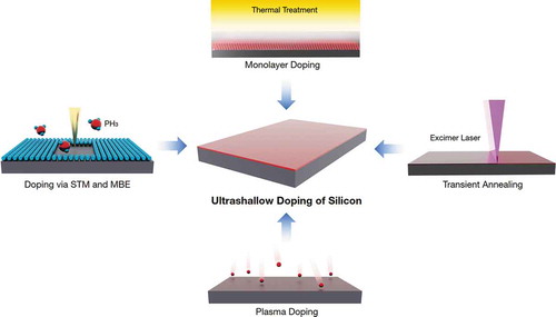
Ultrashallow doping is required for both classical field-effect transistors in integrated circuits and revolutionary quantum devices in quantum computing. In this review, we give a brief overview on recent research advances in three technologies to form ultrashallow doping, namely molecular monolayer doping, molecular beam epitaxy, and low energy ion implantation. A research perspective will be provided at the end of this review.
GRAPHICAL ABSTRACT
Introduction
Dopant atoms are playing a critical role in modern-integrated circuits. As the building blocks of integrated circuits, complementary metal-oxide-semiconductor (CMOS) field-effect transistors are fabricated by introducing dopants to the source and drain region, forming a channel beneath the gate. However, as the size of CMOS transistors scales down, the transistor gate starts to lose its control over the channel to the source and drain that have a deep doping profile [Citation1]. This effect is called as the short channel effect which will cause the failure of CMOS transistors [Citation2,Citation3]. Although new structures such as the ‘FIN’ gate have been widely adopted in modern CMOS transistors to address this issue [Citation4,Citation5], it is still essential to have ultrashallow doping in source and drain to alleviate the short channel effect. For this reason, doping techniques to form ultrashallow junctions (USJs) have been extensively explored in the past decades [Citation6–12]. In addition to classical CMOS transistors, ultrashallow doping has also found applications in deterministic doping at atomic scale for quantum-computing [Citation13–16]. In this article, we assemble a short review of these techniques. We first introduce the research progress and challenges of molecular monolayer doping to form USJs. In the second part, the fascinating development of molecular beam epitaxy for delta doping and single-atom manipulation will be covered. In the end, low energy ion implantation and sub-second annealing techniques for ultrashallow doping will be reviewed before we conclude the review with some research perspectives.
Molecular monolayer doping
Self-assembled molecular monolayer doping (MLD) has attracted intensive research interests due to its capability of facilitating mass production and forming USJs with atomic precision. Based on the well-established self-assembled monolayers (SAMs) grafting technique [Citation17–19], the MLD process was first demonstrated by the Javey group in 2007 [Citation20]. As presented in , dopant-bearing molecules are first covalently bonded to hydrogen-terminated silicon surface via thermal hydrosilylation. The dopants are then driven into bulk silicon and activated during a rapid thermal annealing (RTA) process. To prevent undesired contamination and sublimation of dopant sources during RTA, silicon oxide is deposited as capping layer upon the SAMs.
Figure 1. Illustration of monolayer doping process. Silicon surfaces will be terminated with Si-H after dipping in HF solution. Boron-containing molecules will be grafted on the silicon surfaces via covelent bonds at elevated temperature for hours. SiO2 capping layer is then deposited on the silicon surface to prevent the boron dopants from being driven off the surfaces during the following rapid thermal treatment. Figure adopted from ref [Citation20]
![Figure 1. Illustration of monolayer doping process. Silicon surfaces will be terminated with Si-H after dipping in HF solution. Boron-containing molecules will be grafted on the silicon surfaces via covelent bonds at elevated temperature for hours. SiO2 capping layer is then deposited on the silicon surface to prevent the boron dopants from being driven off the surfaces during the following rapid thermal treatment. Figure adopted from ref [Citation20]](/cms/asset/70d9eb95-179d-4450-acc4-a64ac3bf7bbe/tapx_a_1871407_f0001_oc.jpg)
The diversity of organic molecules and the flexibility of self-assembly process make MLD an attractive and controllable doping technique. Dopants including phosphorus [Citation20–30], boron [Citation8,Citation20,Citation31–34], nitrogen [Citation35], arsenic [Citation27,Citation36] and antimony [Citation37] have been introduced to silicon by MLD using commercial or synthetic reagents.
The areal dose can be modulated by tuning molecule size, monolayer constitutes, reaction time, reaction temperature, and molecular structure. Several strategies on dose modulation have been investigated [Citation20,Citation21,Citation23,Citation24,Citation28,Citation31,Citation37,Citation38]. In the first MLD report, Ho et al [Citation20]. proposed the idea of doping by mixed monolayers constitutes based on steric hindrance effects. ‘Blank precursor’ (1-dodecene) that only contain C and H was used to reduce available reaction sites for boron precursor (allylboronic acid pinacol ester, ABAPE). By tuning the mixing ratio, the density of dopant carrier on final molecular monolayers can be controlled. This method was later studied by Ye et al. systematically () [Citation21]. By mixing diethyl vinylphosphonate (DVP) or ABAPE with 1-dodecene at various ratios, tunable MLD was realized for both n- and p- type dopants. The doping concentration as well as areal doping density can be modulated over 1 order of magnitude. Ultrashallow doping profile can be created with the assistance of spike annealing, where the rapid thermal processing tool is set to reach the peak temperature with high ramping rate (>100 °C/s) without any steady state.
Figure 2. Process flow of mixed monolayer doping method [Citation21]. a) HF etching of native oxide to form a hydrogen-terminated surface; b) Surface functionalization with mixed precursors; c) SiO2 capping layer deposition; d) Thermal annealing for dopant diffusion and subsequent removal of capping layer with HF solution
![Figure 2. Process flow of mixed monolayer doping method [Citation21]. a) HF etching of native oxide to form a hydrogen-terminated surface; b) Surface functionalization with mixed precursors; c) SiO2 capping layer deposition; d) Thermal annealing for dopant diffusion and subsequent removal of capping layer with HF solution](/cms/asset/e6d9ddee-afad-4e8a-a5b2-b2431eedd90d/tapx_a_1871407_f0002_oc.jpg)
The dose modulation can be also achieved by designing specific dopant-bearing molecules. Higher doping levels can be achieved using MLD with precursor carrying more than one dopant. For example, carborane derivatives synthesized with each molecule contains 10 boron atoms has been applied in MLD of silicon and results in a 10-times increase in doping dose compared to the commonly used ABAPE precursor [Citation31]. As presented in , polymers with narrow molecular weight distribution can be used to tune the footprint of precursors, and hence the areal density of dopant distribution. Wu et al. designed hyperbranched polyglycerols with each one carrying only one phosphorus dopant in the core [Citation23,Citation24]. Characterized by nuclear magnetic resonance and dynamic light scattering, the number average molecular weight of the synthesized molecules was found to be approximately 84,000 g/mol with an average diameter around 11 nm. Consequently, the areal dose was significantly reduced to 1.97 × 1011 cm−2 with a maximum doping concentration about 8 × 1016 cm−3. Similarly, Perego et al. synthesized polystyrene (PS) and poly- (methyl methacrylate) polymers (PMMA) end-terminated with a P-containing moiety [Citation28]. The functionalized polymers were first spin-coated on the substrate, followed by a rapid thermal annealing process for surface functionalization. Toluene was used to remove the unattached polymer chains. Before thermal annealing, the functionalized substrate went through a O2 plasma hashing process to minimize carbon contamination. Through repeated cycles of grafting and hashing of phosphorus end-terminated polymers, stepwise increase of the areal dose was achieved. Combined with molar mass manipulation of the synthesized polymers, the authors realized the areal dopant dose modulation. Block copolymer was also reported to achieve a discrete doping of silicon via self-assembly [Citation37]. The dopant-containing small molecules were encapsulated within the core of polystyreneblock-poly(4-vinylpyridine) micelles. The micelles were spontaneously self-assembled on silicon substrate after a spin coating process. Boron and antimony-containing precursors (4-hydroxyphenyl boronic acid pinacol ester and fluoroantimonic acid hexahydrate) were used for supramolecular encapsulation. Ordered B-doped or Sb-doped region was formed after spike-RTA process and the domain spacing can be adjusted by controlling the molar mass of polymers. One issue that may impede further application of polymers in MLD is the incorporation of numerous-unwanted elements (i.e., C, N) during annealing process due to the complex composition of polymers. These elements may lead to the formation of defects and in turn, affects the electrical activation rate of dopants.
Figure 3. Tunable monolayer doping with synthesized macromolecular dopant carriers. a) hyperbranched polyglycerols [Citation23] b) PS and PMMA polymers [Citation28] and c) block copolymers [Citation37]
![Figure 3. Tunable monolayer doping with synthesized macromolecular dopant carriers. a) hyperbranched polyglycerols [Citation23] b) PS and PMMA polymers [Citation28] and c) block copolymers [Citation37]](/cms/asset/b561c4c8-fd50-4fdb-b745-18a85b84c9af/tapx_a_1871407_f0003_oc.jpg)
The carbon-related defects in phosphorus-doped silicon by MLD was investigated using deep level transient spectroscopy (DLTS) and low-temperature Hall measurements in 2018 [Citation22]. The results show that part of phosphorus dopants will bind with interstitial carbon atoms, forming deep level Ci-Ps defects. The probability of forming Ci-Ps pairs is affected by the relative concentration of phosphorus and carbon. For highly doped samples in which both the phosphorus and carbon concentration near surfaces are around 1018 cm−3, 20% of the doped phosphorus will be deactivated due to the formation of Ci-Ps defects. If the concentration of phosphorus is much lower than that of carbon, the deactivation rate will be much higher. Wu et al. prepared lightly P-doped sample via self-assembly of hyperbranched polyglycerols. The concentration of phosphorus near surface was at 1016 cm−3, nearly two orders of magnitude lower than that of carbon. Their results show 73% of the P dopants were deactivated by forming Ci-Ps defects. Efforts have been made in eliminating carbon contamination, including low-temperature oxidation of SAMs [Citation38], application of SiO2 spacer layer [Citation26] and thermally induced P-C bond cleavage [Citation29,Citation39]. However, these methods has limited effects on lightly doped samples. Future work should put emphasis on synthesizing novel carrier molecules that do not contain any carbon.
While carbon impurities have significant influence on the activation of phosphorus dopant, recent research reveals that they have limited impact on boron-doped samples via MLD [Citation32]. Investigated by DLTS and minority carrier transient spectroscopy, Gao et al [Citation32,Citation34] found that carbon-related defects are in form of CsH and CsOH, which act as minority carrier traps. The majority carrier traps were found in form of Bs-O2i, which exist at a low level (less than 1%) and can be potentially suppressed by carbon impurities. Secondary Ion Mass Spectroscopic (SIMS) and Hall measurements showed that the activation rate of boron in silicon by MLD is almost 100%.
Nitrogen-containing chemical reagents need to be used with caution as well. Guan et al [Citation35]. characterized N and P co-doped Si samples via MLD by SIMS and low temperature Hall effect measurement. The results show that the electrical activation rate for both N and P dopants are merely ~1%. Considering an ionization rate of 90% for phosphorus-doped sample by MLD, this outcome was likely due to the presence of nitrogen impurities during the doping process. After all, nitrogen was reported to retard the activation of phosphorus by forming inactive complexes with phosphorus at a ratio of 1:1 [Citation40].
One of the major applications of MLD is the fabrication of USJs. Wafer-scale sub-5 nm junction was fabricated by MLD with the assistance of spike annealing, as depicted in [Citation8]. ABAPE and diethyl 1-propylphosphonate (DPP) were used as B and P sources, respectively. Surface concentration in the order of 1020 was found for spike annealed P-doped sample with peak temperature ranging from 900 to 1050 °C. The junction abruptness was found to be ~7 nm/dec for sample annealed at 1000 °C (), which is a huge leap compared to results obtained using conventional annealing methods in other literature [Citation21,Citation22]. However, the abruptness of doping profile is at the expense of a low dopant incorporation rate, that is, the majority dopants in the monolayer do not diffuse into silicon. Transient annealing techniques such as flash annealing (FLA) and pulsed laser annealing (PLA) are recommended in the field of MLD in silicon to further improve the doping concentration and dopant incorporation rate.
Figure 4. a) Process of USJ formation via MLD with assistance of spike annealing and b) corresponding SIMS results. Adopted from ref [Citation8]
![Figure 4. a) Process of USJ formation via MLD with assistance of spike annealing and b) corresponding SIMS results. Adopted from ref [Citation8]](/cms/asset/d6c10dd8-5217-4b3f-a05b-3c04da8ba9f4/tapx_a_1871407_f0004_oc.jpg)
a) Process of ultrashallow junction formation via MLD with assistance of spike annealing and b) corresponding SIMS results. Adopted from Ref [Citation8].
Delta doping by STM-based hydrogen lithography
The growth of delta-doped layer in silicon via molecular beam epitaxy (MBE) has been intensively investigated for decades. Dopant species such as B, P, Sb, As have been successfully incorporated into silicon epitaxial layer, forming a delta-doped layer on silicon surface. Benefit from geometric constraints, electrical saturation can be avoided due to the inhibition of donor-pair defects formation in silicon [Citation41]. Previous reports have shown a 100% activation rate for planar doping with a doping concentration at the order of 1014 cm−2 [Citation41–43].
In recent years, this method has been revisited thanks to the wide research interest in solid-state quantum computing. In 1998, Kane proposed a silicon-based quantum computing device based on the spin coupling of two phosphorus dopant atoms in silicon [Citation13]. Fabrication of this sort of devices requires the control of phosphorus atoms with atomic precision, which is beyond the processing capacity of conventional equipment. Scanning tunneling microscopy (STM) is one of the few methods capable of manipulating single atoms. The STM-based hydrogen lithography was developed in 2001 to manipulate the adsorption of phosphorus carrier on hydrogen-passivated Si (001) surface [Citation44], as displayed in . In this method, a biased STM tip is used to desorb individual hydrogen atoms on a hydrogen-terminated silicon surface under UHV. The patterned surface will then be exposed to phosphine gas where the resultant silicon dangling bonds can react with phosphine molecules. Phosphorus atoms are then incorporated into silicon surface layer with low temperature (200–300 °C) annealing to minimize diffusion while leaving the hydrogen resist intact. The dissociation and incorporation process of absorbed phosphine molecules is explained by Fuechsle et al. as illustrated in [Citation45]. Through in-situ observation of the heating process, the authors found that three adjacent-desorbed dimers (pairs of silicon surface atoms) along one dimer row secure the doping of one phosphorus atoms. At room temperature, PH3 molecules dissociate into PH2 and H within three dimer sites under high dose rates, which in turn inhibits further reactions. While rising the temperature to 350 °C will lead to the recombination of one PH2 fragment with one hydrogen atom and subsequent desorption from silicon surface. The free silicon site formed during the process will be occupied rapidly through the dissociation of another PH2 into PH and H. The dissociation of PH into P and H will be inhibited until the recombination of the remaining PH2 and hydrogen atom. Maintaining at 350 °C, the resulting phosphorus atom will finally substitute one of the six silicon atoms within the three-dimer patch.
Figure 5. Schematic of STM-based hydrogen lithography process. Figure a-f illustrate the creation of phosphorus atomic devices in silicon. Adopted from ref [Citation43]
![Figure 5. Schematic of STM-based hydrogen lithography process. Figure a-f illustrate the creation of phosphorus atomic devices in silicon. Adopted from ref [Citation43]](/cms/asset/aacb75bb-3d3f-4993-a200-354e54353b5a/tapx_a_1871407_f0005_oc.jpg)
Figure 6. Schematic of the successive dissociation process of phosphine molecules and the subsequent deterministic incorporation of single phosphorus dopant into Si(001) during hydrogen lithography [Citation45]
![Figure 6. Schematic of the successive dissociation process of phosphine molecules and the subsequent deterministic incorporation of single phosphorus dopant into Si(001) during hydrogen lithography [Citation45]](/cms/asset/9c1e05d7-8056-4182-a2b6-113ad6dfa537/tapx_a_1871407_f0006_oc.jpg)
The incorporated phosphorus dopants are then encapsulated in high-quality epitaxial silicon to avoid interfacial effects. Before that, a critical anneal would be performed at 550 °C for 5 min for the desorption of any hydrogen atoms. To minimize dopant diffusion and segregation, silicon epitaxy is more inclined to conduct at lower temperature. Oberbeck et al. fabricated phosphorus delta-doped silicon with 25-nm-thick epitaxial intrinsic silicon layer grown at either 250 °C or room temperature [Citation46]. Segregation lengths of less than 1 nm were obtained for encapsulated phosphorus with silicon overgrowth at 250 °C and room temperature using STM facilities. Although a larger surface roughness was observed for room temperature epitaxial growth, which is mainly due to the smaller mobility of silicon atoms on low-temperature substrate. For samples prepared at 250 °C, Hall effect measurements show a 100% activation of P dopants with electron mobility up to 102 cm2/(V·s) at 4.2 K. A more systematic research was performed by McKibbin et al. in 2009 [Citation47]. P delta-doped samples with silicon encapsulation temperature of 250, 270, 285, and 300 °C were prepared and characterized with STM and magneto-transport. A critical temperature of 270 °C was found for the growth of silicon overlayer. A negligible flatness improvement was observed among all the growth temperature, as indicated in the STM image (). Meanwhile, electrical measurements show a reduction in phosphorus activation rate for growth temperature above 270 °C. At growth temperature of 300 °C, the active carrier density drops by ~50% from 2.4×1014 cm−2 to 1.2×10¹⁴
cm−2. This phenomenon could be explained by the dopant segregation and the subsequent broadening of doping profile at higher growth temperature.
Figure 7. The quality of regrowth surface after encapsulation of phosphorus delta-layers was investigated using STM. Dopants were encapsulated with 25 nm of Si at temperature of (a) 250 °C, (b) 270 °C, (c) 285 °C and (d)300 °C. While negligible flatness improvement was observed for elevated temperature, overgrowth temperature above 270 °C leads to dopants segregation and deactivation [Citation47]
![Figure 7. The quality of regrowth surface after encapsulation of phosphorus delta-layers was investigated using STM. Dopants were encapsulated with 25 nm of Si at temperature of (a) 250 °C, (b) 270 °C, (c) 285 °C and (d)300 °C. While negligible flatness improvement was observed for elevated temperature, overgrowth temperature above 270 °C leads to dopants segregation and deactivation [Citation47]](/cms/asset/57fd0ef1-c982-4fb7-a71d-860b46fb6340/tapx_a_1871407_f0007_oc.jpg)
The thickness of encapsulation layer also plays an important role on dopant activation. Polley et al [Citation48]. used a four-point probe STM to characterize in-situ the sheet resistance of delta-doped layers with different encapsulation thicknesses. As displayed in , the sheet resistance of the delta-doped layer dramatically increases as the encapsulation thickness drops below 5 nm, and completely turns into electrical inactiveness at the thickness of 0.5 nm. This phenomenon could be qualitatively explained by the model of dopant segregation and surface scattering.
Figure 8. The resistivity of phosphorus delta-layer dramatically increases with reducing encapsulation thickness. This depth-dependent conductivity of delta-layer can be explained by the model of dopant segregation and surface scattering [Citation48]
![Figure 8. The resistivity of phosphorus delta-layer dramatically increases with reducing encapsulation thickness. This depth-dependent conductivity of delta-layer can be explained by the model of dopant segregation and surface scattering [Citation48]](/cms/asset/38ffa50d-abbe-42ad-8f0c-fbab5fda1736/tapx_a_1871407_f0008_oc.jpg)
Super-saturation doping is another research interest in the field of delta-doping in silicon. As mentioned above, the phosphorus atoms are incorporated into silicon lattice followed by the spontaneous dissociation of PH3 molecules into PH2, PH and H. For a saturation dosing of reactive sites of 1 monolayer (ML) of Si (001) surface, the theoretical maximum value of total phosphorus coverage is around 0.35 ML. Despite that, the actual P coverage falls short of the theoretical value to around 0.25 ML due to the partial recombination of P species and H in the hydrogen resist removal process where the reaction product desorbs as PH2. To utilize the rest 25% of the reaction sites, a double dose strategy is proposed by McKibbin et al. in 2014 [Citation49]. After the first incorporation annealing of phosphorus at 550 °C, the silicon surface was re-exposed to PH3 gases. A second incorporation annealing at 350 °C was then performed, followed by the dopant encapsulation with 25-nm-thick intrinsic silicon layer at 250 °C. Electrical and STM measurements show the free carrier density up to (3.6 ± 0.1)×1014 cm−2, which means a 50% increase compared to previous records. Stacking of multiple Si:P delta-layers is another strategy for improving active carrier density in silicon. To prevent dopant segregation between multilayers and the formation of P-P dimers, intrinsic silicon spacer layers are introduced to guarantee the phosphorus activation rate. The challenge is to trade off the high-temperature required for high-quality silicon encapsulation and the low-temperature required for dopants confinement. To provide an ideal starting surface for the growth of spacer layer, McKibbin et al [Citation50]. found that the first incorporation annealing at 550 °C is needed to remove the absorbed PHx fragments and H atoms and activate the diffusion of ejected Si diatoms. However, annealing at high temperature will lead to the loss of phosphorus concentration, mainly due to the recombination of PH2 species and H atoms above 360 °C and the subsequent desorption of the resultant PH3. Compared to incorporation annealing at 350 °C, the carrier density of the sample annealed at 550 °C decreases from 2.4×10¹⁴
to 1.9×10¹⁴
cm−2. Nevertheless, a total carrier density of 4.35×10¹⁴
cm−2 was achieved for a double delta-doped sample. Following the same pathway, triple delta-doped layers were successfully fabricated by Keizer and coworkers [Citation51]. The impact of the encapsulated spacer layer on multilayer phosphorus activation was systematically investigated for different spacer layer thickness. Increasing the thickness of intervening silicon between the delta-doping layers can inhibit the segregation of dopants and minimize the formation of P-P dimers. With a spacer layer thickness of 5 nm, an active carrier density up to
4.5×1014 cm−2 was achieved.
While MBE doping method can easily surpass solid solubility of silicon and achieve ultrahigh doping concentration, the integration of this method with CMOS process is problematic due to the requirements of UHV operating environment and the difficulties of mass production.
Ion implantation and advanced annealing techniques
Ion implantation is currently the most common method for introducing dopants in silicon. For ultrashallow doping of silicon, extremely low implantation energy is required to reduce the ions projection range. Under such circumstance, channeling effect is more pronounced. As the energy decreases, the possibility of ions scattered into channels increases, which results in broadening and formation of longer tails of the final doping profile. Strategies like pre-amorphization or amorphization are commonly used to mitigate the channeling issue. However, the amorphization of semiconductor surface may lead to the formation of end-of-range defects, which could further result in the transient-enhanced diffusion of implanted dopants during followed thermal annealing process.
Lower implantation energy often comes with a lower beam current, which leads to an undesirably longer exposure period and lower throughput. This issue is more prominent in USJ fabrication, where a higher implantation dose is required to reduce series resistances as the junction thickness decreases. The space charge effect also manifest itself at extremely low implantation energy, which would result in beam expansion and dose variation. Indeed, several strategies have been proposed to eliminate the space charge effect, including beam neutralization [Citation52,Citation53], deceleration mode [Citation6,Citation54], molecular implantation [Citation55–57], etc. The challenge still exists for beamline implanters to operate at extremely low implantation energy whilst maintaining high throughput.
Plasma doping have been introduced as an alternative to beamline implantation for its high-throughput and low-cost [Citation58–60]. Different from beamline implanter, herein, the target wafer is directly placed inside the plasma of ion sources during the implantation process. By applying a pulsed voltage on the target wafer, ions in the plasma will be extracted and accelerated across the sheath. Dopant ions are implanted into the superficial layer of semiconductors at extremely low energies. Thus, plasma doping can realize the simultaneous implantation of whole wafer in nature. However, several drawbacks have hindered its wider application. For instance, the absence of mass separation components of plasma doping may lead to potential contamination issue. In principle, plasma doping is a complicated process with a combination of ion implantation, etching, and ion beam deposition. These features make it challenging to predict the accurate doping profile for plasma doping.
The fabrication of USJ relies on both the as-implant doping profile and the dopant diffusion during thermal activation. Annealing technique is another hot topic in the research of ultra-shallow doping. The desire to maximize dopant activation with minimized diffusion in USJ fabrication has reignited the research interests in subsecond annealing techniques such as FLA [Citation61–64] and PLA [Citation62,Citation65–69] that were first proposed in late 1970s [Citation70,Citation71].
PLA, a transient annealing technique, has shown its potential in numerous state-of-the-art semiconductor manufacturing, especially the thermal annealing of ion-implanted silicon. In PLA, an ultra-short pulse laser is utilized to irradiate semiconductors, injecting massive energy into the semiconductor surface, which increases the surface temperature to more than 1000 °C in nano or picoseconds. The temperature will rapidly drop to room temperature within sub-microseconds depending on the thermal conductivity of the semiconductors. For Si, the quenching rate could reach to 1010 K/s. The extremely short thermal driving time makes PLA an effective technique to eliminate dopant diffusion in semiconductors compared to conventional thermal treatments.
As a subset of PLA, excimer laser annealing (ELA) has attracted lots of attention due to the high absorption coefficient of silicon at UV wavelength. As a result, the absorption of light energy is limited to a few nanometers from the surface. A. Scheit et al. compared the ELA technique with spike annealing and FLA by evaluating the sheet resistance, taking transmission electron microscopy (TEM) images and performing dopant profiling of the annealed ion-implanted sample [Citation62]. ArF excimer laser with a wavelength of 193 nm and a duration of 25 ns was used by A. Scheit et al. The experimental wafer was first pre-amorphized with germanium ion-implantation, followed by ion-implantation of either boron or arsenic. The results show that ELA is superior to competing technologies on B-doped samples. As shown in , B-implanted samples annealed at an energy density of 400 mJ/cm2 for 32 pulses exhibit an ultrahigh abruptness of 2.5 nm/dec at the amorphous/crystalline interface, which is 4–10 times narrower than the results obtained by spike annealing or FLA. This phenomenon can be explained by the elimination of transient-enhanced diffusion of boron benefited from ultrahigh ramping and quenching rate of ELA process. While for As-doped sample, ELA does not show great advantages compared to other methods. ELA cannot dissolve all the defects within ion-implanted sample, even with an energy density up to 600 mJ/cm2.
Figure 9. ArF excimer laser with pulse energy density varies from 300 to 600 mJ/cm2 was used for the annealing of boron ion-implanted silicon. B-implanted samples annealed at 400 mJ/cm2 for 32 pulses per point exhibit an ultrahigh abruptness of 2.5 nm/dec at the amorphous/crystalline interface [Citation62]
![Figure 9. ArF excimer laser with pulse energy density varies from 300 to 600 mJ/cm2 was used for the annealing of boron ion-implanted silicon. B-implanted samples annealed at 400 mJ/cm2 for 32 pulses per point exhibit an ultrahigh abruptness of 2.5 nm/dec at the amorphous/crystalline interface [Citation62]](/cms/asset/6a66fe8b-39f5-40c9-b7a4-d7503b2d02b5/tapx_a_1871407_f0009_oc.jpg)
Alba et al [Citation72]. investigate the ELA of phosphorus implanted silicon-on-insulator (SOI) wafer with a device layer thickness of 22 nm. Phosphorus ions were implanted into the device layer where an amorphous layer of 9.5 nm thick was created, as indicated in the TEM image shown in . The ion-implanted samples were annealed using a XeCl ELA system at a wavelength of 308 nm and a pulse duration of 160 ns. The amorphous layer is recrystallized at pulse energy density around 0.65 J/cm2 due to the melting of amorphous layer with a high density of extended defects (). Increasing the energy density could further extend the liquid/solid interface and reduce defects formation. At 0.85 J/cm2, the liquid/solid interface has reached to crystalline region, which leads to the epitaxial regrowth of melted layer during recrystallization process, as displayed in .
Figure 10. Cross sectional TEM micrographs of P-implanted SOI with device layer of 22 nm after removal of capping layers, before and after XeCl ELA process. TEM images illustrate the evolution of crystallinity of device layer with elevated energy density, a) as-implanted, after ELA at b) 0.65 J/cm2, c) 0.75 J/cm2, d) 0.85 J/cm2 and 0.91 J/cm2 [Citation72]
![Figure 10. Cross sectional TEM micrographs of P-implanted SOI with device layer of 22 nm after removal of capping layers, before and after XeCl ELA process. TEM images illustrate the evolution of crystallinity of device layer with elevated energy density, a) as-implanted, after ELA at b) 0.65 J/cm2, c) 0.75 J/cm2, d) 0.85 J/cm2 and 0.91 J/cm2 [Citation72]](/cms/asset/f824c00d-a5cc-4af6-85b5-aa555bd4ad18/tapx_a_1871407_f0010_oc.jpg)
Nevertheless, the above-mentioned works all involve the melting of ion-implanted region where merely a box-like dopant profile could be obtained. To maintain the as-implanted dopant profile and minimize dopant diffusion, Florakis et al [Citation69]. investigated the non-melt ELA of plasma implanted boron-doped substrate. Ultrashallow dopant profile was created by BF3 plasma implantation with an impinge energy of 0.4 keV and a dose of 3×1015 cm−2. KrF excimer laser was used to irradiate the sample surface with energy density ranging from 375 to 640 mJ/cm2. SIMS results in show negligible difference in boron profile between the as-implanted and laser-annealed sample, indicating that the annealing of sample surface is in the non-melt regime. Further characterizations with TEM show that for samples annealed at an energy density of 575 mJ/cm2 for 50 pulses, the former ion-implanted amorphous region has completely recrystallized. The corresponding sheet resistance around 1.6 kΩ/sq also indicates a considerable boron activation in doped region. The research group further worked on simulation of plasma doping and ELA process using Synopsys Sentaurus Process software tool and Kinetic Monte Carlo approach [Citation66]. The calculated results is in good agreement with experimental data. For sample annealed at 625 mJ/cm2 for 50 pulses, the measured sheet resistance drops to 680 Ω/sq from initial value of 15 kΩ/sq. Considering the minimum theoretical value is around 550 Ω/sq, the non-diffusion activation of dopants seems promising using ELA in non-melting region.
Figure 11. SIMS profiles of boron before and after non-melt ELA process on plasma implanted boron-doped substrate. Samples were annealed using KrF excimer laser with energy density of 510 and 575 mJ/cm2. The negligible difference in boron profiles suggests the ELA in non-melt region [Citation69]
![Figure 11. SIMS profiles of boron before and after non-melt ELA process on plasma implanted boron-doped substrate. Samples were annealed using KrF excimer laser with energy density of 510 and 575 mJ/cm2. The negligible difference in boron profiles suggests the ELA in non-melt region [Citation69]](/cms/asset/a6172468-e812-4888-8216-eec198267350/tapx_a_1871407_f0011_oc.jpg)
Somehow, the adoption of ion implantation has limited the flexibility of ELA process. Since ELA is used for elimination of implantation-induced defects and dopant activation, the resulting dopant profile is dependent on the ion-implantation parameters. Popadic et al [Citation73]. explored the possibility of fabricating USJs in silicon by combining CVD deposited arsenic monolayer with ELA. After the formation of arsenic monolayer on silicon surface by RPCVD, the sample was directly irradiated with XeCl excimer laser at a wavelength of 308 nm for 25 ns. The energy density ranging from 600 to 1100 mJ/cm2 was used to melt silicon surfaces and drive-in arsenic dopants. ~ 10 nm deep USJs were fabricated with a sheet resistance lower than 100 Ω/sq. This doping strategy was further optimized by Lorito et al [Citation67]. After the growth of arsenic monolayer, a thin layer of TiN was deposited on the as-fabricated silicon surface by physical vapor deposition as the capping layer. The UV transparent material TiN was used to prevent the volatilization of the arsenic precursor and surface oxidation.
Microwave annealing (MWA) is another promising technique for low-temperature crystallization of amorphous silicon and dopant activation while minimizing dopant diffusion. Benefited from its insensitivity to surface reflectivity variations, MWA has been treated as an alternative to millisecond annealing technique. In 2007, Thompson at al [Citation74]. demonstrated the healing of ion-implantation-indued amorphous silicon by MWA. Silicon wafer implanted with either boron or arsenic at the doses ranging from 1×10¹⁴ to 5×10¹⁵
cm−2 was treated by MWA at a fixed frequency of 2.45 GHz and a power of 1300 W for various processing time. Note that for arsenic-doped samples, SiC susceptors were used to generate the required higher temperature for dopant activation. After the MWA process, the authors characterized the microstructure with XTEM, finding that the damaged crystalline structure of the implanted silicon is repaired, consistent with the dramatic decrease in sheet resistance of the sample. The repair of the crystalline structure is likely caused by solid-phase epitaxial regrowth. Alford [Citation75] pointed out that the fixed-frequency MWA may cause non-uniform heating due to the establishment of standing wave patterns in the processing chamber. Therefore, a variable frequency microwave was used for MWA by sweeping a bandwidth of frequencies at short intervals of 0.1 second, resulting in a uniform heating of implanted wafer. The damaged arsenic-doped sample was repaired at a surface temperature lower than 550 °C for the processing time of ~ 6 min. Lee et al [Citation76]. instead continued to address the non-uniform heating issue of the fixed-frequency MWA. By systematically investigating the composition, number and spacing of susceptors around process wafers, the authors found an optimized solution by placing a susceptor wafer adjacent to the implanted sample. Xu et al [Citation77]. also reported the formation of USJs using MWA in 2013. To enhance the microwave absorption and shorten the ions projection range, the silicon wafer was pre-amorphized with Ge prior to ion implantation of boron or arsenic. Their results show a complete solid phase regrowth at substrate temperature lower to 440 °C. However, the elimination of end-of-range (EOR) defects requires a higher processing temperature. MWA at 3500 W (corresponding to a peak substrate temperature of 570 °C) can greatly reduce EOR defects but at a cost of dopant deactivation. The activation rate of only 13% and 32% were achieved for boron and arsenic implanted sample, respectively. Zhao et al [Citation78]. later reported a higher activation rate of 64% for P+ implants with negligible dopant diffusion. They demonstrated the superiority of MWA over RTP on dopant activation at low temperature with similar thermal budgets, which could be explained by the localized hopping of ions into adjacent vacancies in the presence of microwave field.
Summary and perspective
Each doping technique has its own pros and cons which are summarized in . Ultrashallow doping which allows the delicate control on dopant concentration and spatial distribution will benefit not only the development of next-generation CMOS process, but also the interesting research on future solid-state quantum computing. The above-mentioned methods are all promising candidates for ultrashallow doping of semiconductors. However, there are still many issues to address before these techniques find commercial applications.
Table 1. Pros and Cons of different doping techniques
MLD utilizes the self-limited property of silicon surface on the formation of dopant-containing monolayers. As a result, the doses can be modified by tuning the molecular size. However, the thermal annealing process for dopant driving-in is problematic with a trade-off in dopant diffusion depth and incorporation rate. The prolonged high temperature required for liquid phase reaction for monolayer formation is also a serious concern for commercial applications. Furthermore, the organic precursors with complex elemental composition used in MLD bring uncertainty to the dopant activation rate. Future research on MLD should focus on the development of sub-second annealing techniques, gas phase formation of monolayers, along with the design and synthesis of gas precursors with electronic grade purity.
The mechanism on the growth of delta-doped layer in silicon by MBE has been well-understood thanks to the combination with STM. In principle, MBE doping method can create perfect 2D dopant layer in silicon that surpass its solid solubility and achieve ultrahigh carrier density with 100 % dopant activation rate. Even so, it is challenging to integrate this method with CMOS process.
For ion-implantation method, the fabrication of USJs relies on both the as-implant doping profile and the dopant diffusion during thermal activation. While low energy ion implantation, as well as plasma doping, has already commercially used in the industries, there are still many issues lies in the annealing techniques. For example, PLA and FLA suffer from the temperature inhomogeneity caused by the surface reflectivity in patterned substrates. For MWA, there is large room to improve dopant activation and eliminate defects.
Disclosure statement
No potential conflict of interest was reported by the authors.
Additional information
Funding
References
- Brews JR, Fichtner W, Nicollian EH, et al. Generalized guide for MOSFET miniaturization. IEEE Electr Device L. 1980;1:2–25.
- Sze SM. Physics of semiconductor devices: physics and technology. 2nd ed. New York: Wiley; 2001.
- Neamen DA. Semiconductor physics and devices: basic principles. New York, NY: McGraw-Hill; 2012.
- Hisamoto D, Lee WC, Kedzierski J, et al. A folded-channel MOSFET for deep-sub-tenth micron era. International Electron Devices Meeting 1998. Technical Digest (Cat. No.98CH36217), San Francisco, CA, USA. 1998 6-9 Dec. 1998.
- Hisamoto D, Wen-Chin L, Kedzierski J, et al. FinFET-a self-aligned double-gate MOSFET scalable to 20 nm. IEEE Trans Electron Devices. 2000;47:2320–2325.
- Hong S, Ruggles G, Paulos J, et al. Formation of ultrashallow p+‐n junctions by low‐energy boron implantation using a modified ion implanter. Appl Phys Lett. 1988;53:1741–1743.
- Kim SD, Park CM, Woo JCS. Advanced source/drain engineering for box-shaped ultrashallow junction formation using laser annealing and pre-amorphization implantation in sub-100-nm SOI CMOS. IEEE Trans Electron Devices. 2002;49: 1748–1754
- Ho JC, Yerushalmi R, Smith G, et al. Wafer-scale, Sub-5 nm junction formation by monolayer doping and conventional spike annealing. Nano Lett. 2009;9:725–730.
- Wang Q, Osburn CM, Canovai CA. Ultra-shallow junction formation using silicide as a diffusion source and low thermal budget. IEEE Trans Electron Devices. 1992;39:2486–2496.
- Baik S, Kwon DJ, Kang H, et al. Conformal and ultra shallow junction formation achieved using a pulsed-laser annealing process integrated with a modified plasma assisted doping method. IEEE Access. 2020;8:172166–172174.
- Sarubbi F, Nanver LK, Scholtes TL. CVD delta-doped boron surface layers for ultra-shallow junction formation. ECS Trans. 2006;3:35.
- Chuang S, Cho T, Sung P, et al. Ultra-shallow junction formation by monolayer doping process in single crystalline Si and Ge for future CMOS devices. ECS Journal of Solid State Science and Technology. 2017;6:350–355
- Kane BE. A silicon-based nuclear spin quantum computer. Nature. 1998;393:133–137.
- Schofield SR, Curson NJ, Simmons MY, et al. Atomically precise placement of single dopants in Si. Phys Rev Lett. 2003;91:136104.
- Koch M, Keizer JG, Pakkiam P, et al. Spin read-out in atomic qubits in an all-epitaxial three-dimensional transistor. Nat Nanotechnol. 2019;14:137–140.
- Veldhorst M, Yang CH, Hwang JC, et al. A two-qubit logic gate in silicon. Nature. 2015;526:410–414.
- Linford MR, Chidsey CED. Alkyl monolayers covalently bonded to silicon surfaces. J Am Chem Soc. 1993;115:12631–12632.
- Wasserman SR, Tao YT, Whitesides GM. Structure and reactivity of alkylsiloxane monolayers formed by reaction of alkyltrichlorosilanes on silicon substrates. Langmuir. 1989;5:1074–1087.
- Sieval AB, Demirel AL, Nissink JWM, et al. Highly stable Si-C linked functionalized monolayers on the silicon (100) surface. Langmuir. 1998;14:1759–1768.
- Ho JC, Yerushalmi R, Jacobson ZA, et al. Controlled nanoscale doping of semiconductors via molecular monolayers. Nat Mater. 2007;7:62–67.
- Ye L, Pujari SP, Zuilhof H, et al. Controlling the dopant dose in silicon by mixed-monolayer doping. ACS Appl Mater Interfaces. 2015;7:3231–3236.
- Gao X, Guan B, Mesli A, et al. Deep level transient spectroscopic investigation of phosphorus-doped silicon by self-assembled molecular monolayers. Nat Commun. 2018;9:118.
- Wu H, Li K, Gao X, et al. Phosphorus ionization in silicon doped by self-assembled macromolecular monolayers. AIP Adv. 2017;7:105310.
- Wu H, Guan B, Sun Y, et al. Controlled doping by self-assembled dendrimer-like macromolecules. Sci Rep. 2017;7:41299.
- Alphazan T, Mathey L, Schwarzwälder M, et al. Monolayer doping of silicon through grafting a tailored molecular phosphorus precursor onto oxide-passivated silicon surfaces. Chem Mater. 2016;28:3634–3640.
- van Druenen M, Collins G, Glynn C, et al. Functionalization of SiO2 surfaces for Si monolayer doping with minimal carbon contamination. ACS Appl Mater Interfaces. 2018;10:2191–2201.
- O’Connell J, Collins G, McGlacken GP, et al. Monolayer doping of Si with improved oxidation resistance. ACS Appl Mater Interfaces. 2016;8:4101–4108.
- Perego M, Seguini G, Arduca E, et al. Control of doping level in semiconductors via self-limited grafting of phosphorus end-terminated polymers. ACS Nano. 2018;12:178–186.
- Zhi K, Zhang C, Wei H, et al. Thermal pyrolysis investigation of self-assembled molecular monolayer for defect-free doping in silicon. Chem Phys. 2020;531:110658.
- Zhang C, Peng M, Hu W, et al. Toward scalable fabrication of atomic wires in silicon by nanopatterning self-assembled molecular monolayers. ACS Appl Electron Mater. 2020;2:275–281.
- Ye L, González-Campo A, Núñez R, et al. Boosting the boron dopant level in monolayer doping by carboranes. ACS Appl Mater Interfaces. 2015;7:27357–27361.
- Gao X, Kolevatov I, Chen K, et al. Full activation of boron in silicon doped by self-assembled molecular monolayers. ACS Appl Electron Mater. 2020;2:268–274.
- Veerbeek J, Ye L, Vijselaar W, et al. Highly doped silicon nanowires by monolayer doping. Nanoscale. 2017;9:2836–2844.
- Fu J, Chen K, Chang S, et al. Dopant activation and photoresponses of boron-doped silicon by self-assembled molecular monolayers. AIP Adv. 2019;9:125219.
- Guan B, Siampour H, Fan Z, et al. Nanoscale nitrogen doping in silicon by self-assembled monolayers. Sci Rep. 2015;5:12641.
- O’Connell J, Verni GA, Gangnaik A, et al. Organo-arsenic molecular layers on silicon for high-density doping. ACS Appl Mater Interfaces. 2015;7:15514–15521.
- Popere BC, Russ B, Heitsch AT, et al. Large-area, nanometer-scale discrete doping of semiconductors via block copolymer self-assembly. Adv Mater Interfaces. 2015;2:18.
- Wu H, Chen Q, Huang N, et al. Evolution of hyperbranched polyglycerols as single-dopant carriers. Colloids Surf A Physicochem Eng Asp. 2020;592:124608.
- Longo RC, Cho K, Schmidt WG, et al. Monolayer doping via phosphonic acid grafting on silicon: microscopic insight from infrared spectroscopy and density functional theory calculations. Adv Funct Mater. 2013;23:3471–3477.
- Chang R, Lin C. Deactivation of phosphorus in silicon due to implanted nitrogen. physica status solidi (c)). 2014;11: 24–27.
- Citrin PH, Muller DA, Gossmann HJ, et al. Geometric frustration of 2D dopants in silicon: surpassing electrical saturation. Phys Rev Lett. 1999;83:3234–3237.
- Oberbeck L, Curson NJ, Simmons MY, et al. Encapsulation of phosphorus dopants in silicon for the fabrication of a quantum computer. Appl Phys Lett. 2002;81:3197–3199.
- Ruess FJ, Oberbeck L, Simmons MY, et al. Toward atomic-scale device fabrication in silicon using scanning probe microscopy. Nano Lett. 2004;4:1969–1973.
- O’Brien JL, Schofield SR, Simmons MY, et al. Towards the fabrication of phosphorus qubits for a silicon quantum computer. Phys Rev B. 2001;64:161401.
- Fuechsle M, Miwa JA, Mahapatra S, et al. A single-atom transistor. Nat Nanotechnol. 2012;7:242–246.
- Oberbeck L, Curson NJ, Hallam T, et al. Measurement of phosphorus segregation in silicon at the atomic scale using scanning tunneling microscopy. Appl Phys Lett. 2004;85:1359–1361.
- McKibbin SR, Clarke WR, Simmons MY. Investigating the surface quality and confinement of Si: pδ-layers at different growth temperatures. Physica E. 2010;42:1180–1183.
- Polley CM, Clarke WR, Miwa JA, et al. Exploring the limits of N-type ultra-shallow junction formation. ACS Nano. 2013;7:5499–5505.
- McKibbin SR, Polley CM, Scappucci G, et al. Low resistivity, super-saturation phosphorus-in-silicon monolayer doping. Appl Phys Lett. 2014;104:123502.
- McKibbin SR, Clarke WR, Fuhrer A, et al. Optimizing dopant activation in Si:P double δ-layers. J Cryst Growth. 2010;312:3247–3250.
- Keizer JG, McKibbin SR, Simmons MY. The impact of dopant segregation on the maximum carrier density in Si: P Multilayers. ACS Nano. 2015;9:7080–7084.
- Mack M. Charging and charge neutralization in ion implantation. Nucl Instrum Methods Phys Res, Sect B. 1989;37:472–477.
- Liu F, Monteiro O, Yu K, et al. Self-neutralized ion implantation into insulators. Nucl Instrum Methods Phys Res, Sect B. 1997;132:188–192.
- White N, Chen J, Mulcahy C, et al., Chicane deceleration—an innovative energy contamination control technique in low energy ion implantation. AIP Conference Proceeding, 16th International Conference on Ion Implantation Technology, Marseille, Frances. 2006; 866:1, 335-339.
- Beanland DG. The behaviour of boron molecular ion implants into silicon. Solid-State Electron. 1978;21:537–547.
- Müller H, Ryssel H, Schmid K. Electrical properties of silicon layers implanted with BF2 molecules. J Appl Phys. 1972;43:2006–2008.
- Wilson H, Prawer S, Spizzirri P, et al. P2 dimer implantation in silicon: a molecular dynamics study. Nucl Instrum Methods Phys Res, Sect B. 2006;251:395–401.
- Mizuno B, Nakayama I, Takase M, et al. Plasma doping for silicon. Surf Coat Technol. 1996;85:51–55.
- Felch SB, Fang Z, Koo BW, et al. Plasma doping for the fabrication of ultra-shallow junctions. Surf Coat Technol. 2002;156:229–236.
- Ensinger W. Semiconductor processing by plasma immersion ion implantation. Mater Sci Eng A. 1998;253:258–268.
- Normann HB, Vines L, Privitera V, et al. Phosphorus in-diffusion from a surface source by millisecond flash lamp annealing for shallow emitter solar cells. Appl Phys Lett. 2013;102:132108.
- Scheit A, Lenke T, Bolze D, et al. Dopant profile engineering using ArF excimer laser, flash lamp and spike annealing for junction formation. 2014 20th International Conference on Ion Implantation Technology (IIT), Portland, Oregon, USA; 2014 2014-06-01: IEEE.
- Riise HN, Schumann T, Azarov A, et al. Formation of shallow boron emitters in crystalline silicon using flash lamp annealing: role of excess silicon interstitials. Appl Phys Lett. 2015;107:022105.
- Kalkofen B, Ahmed B, Beljakowa S, et al. Atomic layer deposition of phosphorus oxide films as solid sources for doping of semiconductor structures. 2018 IEEE 18th International Conference on Nanotechnology (IEEE-NANO), Cork, Ireland; 2018 23-26 July 2018.
- Whelan S, La Magna A, Privitera V, et al. Dopant redistribution and electrical activation in silicon following ultra-low energy boron implantation and excimer laser annealing. Phys Rev B. 2003;67:075201.
- Florakis A, Papadimitriou A, Chatzipanagiotis N, et al. Formation of silicon ultra shallow junction by non-melt excimer laser treatment. Solid-State Electron. 2010;54:903–908.
- Lorito G, Qi L, Nanver L. Arbitrarily shallow arsenic-deposited junctions on silicon tuned by excimer laser annealing. 2010 10th IEEE International Conference on Solid-State and Integrated Circuit Technology, Shanghai, China; 2010 2010-11-01: IEEE.
- Qiu Y, Cristiano F, Huet K, et al. Extended defects formation in nanosecond laser-annealed ion implanted silicon. Nano Lett. 2014;14:1769–1775.
- Florakis A, Misra N, Grigoropoulos C, et al. Non-melt laser annealing of plasma implanted boron for ultra shallow junctions in silicon. Mater Sci Eng, B. 2008;154-155:39–42.
- White CW, Christie WH, Appleton BR, et al. Redistribution of dopants in ion‐implanted silicon by pulsed‐laser annealing. Appl Phys Lett. 1978;33:662–664.
- Wu CP, Magee CW. Pulsed‐laser annealing of ion‐implanted polycrystalline silicon films. Appl Phys Lett. 1979;34:737–739.
- Alba PA, Kerdiles S, Mathieu B, et al. Nanosecond laser annealing for phosphorous activation in ultra-thin implanted silicon-on-insulator substrates. 2016 21st International Conference on Ion Implantation Technology (IIT), Tainan, Taiwan; 2016 2016-09-01: IEEE.
- Popadic M, Nanver LK, Biasotto C, et al. Ultrashallow doping by excimer laser drive-in of RPCVD surface deposited arsenic monolayers. 2008 16th IEEE International Conference on Advanced Thermal Processing of Semiconductors, Las Vegas, NV, USA, 2008, pp. 141–146
- Thompson DC, Decker J, Alford TL, et al. Microwave activation of dopants & solid phase epitaxy in silicon. 2007 MRS Spring Meeting - San Francisco, CA, United States; 989, 0989-A06-18.
- Alford TL, Ahmad I, Hubbard R. Variable frequency microwave induced low temperature dopant activation in ion implanted silicon. 2009 17th International Conference on Advanced Thermal Processing of Semiconductors, Albany, NY, USA; 2009 2009-09-01: IEEE.
- Lee Y, Hsueh F, Current MI, et al. Susceptor coupling for the uniformity and dopant activation efficiency in implanted Si under fixed-frequency microwave anneal. IEEE Electr Device L. 2012;33:248–250.
- Xu P, Fu C, Hu C, et al. Ultra-shallow junctions formed using microwave annealing. Appl Phys Lett. 2013;102:122114.
- Zhao Z, David Theodore N, Vemuri RNP, et al. Effective dopant activation via low temperature microwave annealing of ion implanted silicon. Appl Phys Lett. 2013;103:192103.