
 ?Mathematical formulae have been encoded as MathML and are displayed in this HTML version using MathJax in order to improve their display. Uncheck the box to turn MathJax off. This feature requires Javascript. Click on a formula to zoom.
ABSTRACT
Nanowire networks represent a unique class of neuromorphic systems. Their self-assembly confers a complex structure to their network circuitry, embedding a higher interconnectivity of resistive switching memory (memristive) cross-point junctions than can be achieved with top-down nanofabrication methods. Coupling of the nonlinear memristive dynamics to the network topology enables intrinsic adaptiveness and gives rise to emergent non-local dynamics. In this article, we summarise the physical principles underlying the memristive junctions and network dynamics of neuromorphic nanowire networks and provide the first comprehensive review of studies to date. We conclude with a perspective on future prospects for neuromorphic information processing.
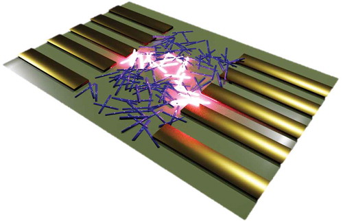
Graphical abstract
1. Introduction
The concept of ‘neuro-inspired’ information processing can be traced back to Alan Turing’s very early ideas on neural networks, as described in his 1948 report ‘Intelligent Machinery’ [Citation1]. Subsequent developments that paved the way for what became known as artificial intelligence (AI) remained largely in the realm of mathematical models until the 1990 publication ‘Neuromorphic Electronic Systems’ [Citation2] by Carver Mead, who proposed a new type of electronic hardware engineered to mimic biological information processing systems (see [Citation3] for a recent recount of Mead’s story). The idea of realising highly efficient neuro-inspired information processing in hardware is significant because biological neural networks are, after all, physical systems, so in principle, it should be possible to emulate neuromorphic functionality in materio.
This vision is now entrained in the paradigm known as neuromorphic engineering of which, propelled by the looming end of Moore’s law, neuromorphic computing is a major focus [Citation4]. Broadly speaking, a common feature of this approach is a neuro-inspired architecture that integrates memory and processing. Exploiting the dramatically improved power efficiency of such beyond von Neumann architectures has enabled the development of neuromorphic chips dedicated to power-hungry AI training [Citation5] and the in silico implementation of neuro-inspired spike-based learning schemes [Citation6–10].
In contrast to conventional silicon-based CMOS chips, an alternate approach to neuro-inspired hardware has been driven by the development of novel non-CMOS nanoelectronic memory devices [Citation11]. Of these, those exhibiting resistive switching memory are especially promising for next-generation neuromorphic systems, offering a considerably reduced area and energy cost of emulating neurons and synapses, compared to silicon-CMOS-based approaches [Citation12–15]. Resistive switching nanoelectronic devices were first proposed as a new class of non-volatile memory [Citation16,Citation17]. Since the subsequent physical realisation of the memristor [Citation18], developments in resistive switching memory (memristive) devices have continued to be made at an increasingly rapid pace, driven by the potential to realise next-generation memories for storage and in-memory computing (e.g. state-full logic applications), as well as analogue circuits and neuromorphic computing [Citation13,Citation14,Citation19]. In particular, the synapse-like nonlinear electrical response of memristors and memristive devices is especially attractive, owing to the ability to replicate diverse brain-like functionalities such as short-term and long-term potentiation (STP/LTP) and spike timing-dependent plasticity (STDP), which are key to learning abilities [Citation19–22]. Indeed, memristive switching may emulate the fast transitions between low and high activity observed in the human cortex that is thought to be central for perception and decision-making [Citation23].
Neuromorphic functionalities at the device level can be attributed to the modification of transport mechanisms by nanoscale geometric confinement, usually across a metal-insulator-metal (MIM) junction. Importantly, synapse-like memristive switching is observed not just in memristors fabricated from conventional bulk materials (e.g. metal oxides) [Citation24], but also in neuromorphic systems self-assembled from low-dimensional sub-lithographic nanomaterials using bottom-up techniques [Citation25]. For example, van der Wiel and colleagues found that disordered assemblies of gold nanoparticles interconnected by insulating molecules are capable of performing Boolean logic functions [Citation26]. In a similar system, they demonstrated nonlinear classification and feature extraction performed in materio [Citation27]. Similar self-assembled nanoparticle networks were shown to exhibit synapse-like resistive switching events near the electrical percolation threshold [Citation28–30]. Subsequent studies by Brown and colleagues [Citation31–33] revealed the neuromorphic nature of these switching events by demonstrating avalanche dynamics similar to that observed in cultured cortical neurons [Citation34]. Other examples of low-dimensional neuromorphic nanomaterials include semiconducting quantum dots, carbon nanotubes [Citation35,Citation36] and other organic neuromorphic devices (see, e.g. [Citation37]), as well as nanostructures comprised of mixed-dimensional heterojunctions (see Sangwan and Hersam [Citation25] for a comprehensive review). Memristive switching in self-assembled nanoelectronic systems, usually due to ionic transport and redox processes, underlies the nonlinear dynamics that indicate the potential for neuromorphic information processing.
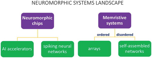
Nanowires represent another class of low-dimensional nanostructures with memristive properties. In the first experimental observation of memristive switching in single metal-oxide nanowires, Kim et al. [Citation38] showed that reversible switching is achieved at much lower voltages in quasi-1D NiO nanowires compared to 2D NiO thin films. Subsequent studies have demonstrated a broad range of memristive switching devices based on metal-oxide nanowire (or nanorod) arrays constructed using bottom-up techniques (see Milano et al. [Citation39] for a comprehensive review). outlines the neuromorphic systems landscape in a way that broadly delineates silicon-based chips and memristive systems. The latter can operate as analogue systems and can be further subdivided into ordered and disordered systems, broadly corresponding to top-down and bottom-up fabrication methods. This is by no means an exclusive subdivision, since one of the most promising technologies for AI hardware implementation, memristor cross-bar arrays, represents a hybrid CMOS/memristive neuromorphic system [Citation40].
Figure 1. Schematic outline of the neuromorphic systems landscape, broadly subdivided by silicon-based neuromorphic chips and beyond-silicon memristive devices, the latter further subdivided into ordered systems (fabricated by top-down methods) and disordered systems (synthesised by bottom-up methods)
This Review focuses on nanowires that self-assemble into a disordered network configuration, with memristive cross-point junctions. Nanowire networks (NWNs) are particularly interesting because collective electrical responses emerge from the complex network structure, drawing strong similarities to the structure–function relation in real (biological) neural networks formed by bottom-up self-assembly [Citation41]. This enables NWNs to perform learning tasks intrinsically, without requiring hardware implementation of an algorithmic artificial neural network learning model. Varying the spatio-temporal input signals (i.e. delivered via different contact electrodes and with time-varying amplitudes) can form new electrical transmission routes, in a manner analogous to synaptogenetic learning [Citation42,Citation43]. Despite their distinctive neuro-synaptic properties, NWNs remain a relatively underexplored class of neuromorphic systems. Thus, here we review the physical principles underlying NWNs, including the mechanisms responsible for memristive switching at their junctions and the non-local dynamics arising from their network structure (Sec. 2). We then summarise the relevant studies and progress to date in Sec. 3 before discussing future prospects for NWNs as neuro-inspired information processing systems (Sec. 4).
2. Physical mechanisms and dynamics
NWNs are readily synthesised using established bottom-up self-assembly methods (e.g. polyol synthesis process for nanowire dispersion [Citation44], followed by drop-casting or spray depositing onto an insulating planar substrate [Citation39]). This naturally produces a 2D spatial distribution of randomly oriented nanowires, interconnected by cross-point MIM junctions, with typical densities of 10 junctions/m2 and 0.5 nanowires/
m2 [Citation45,Citation46]. Device electrodes can also be mask-deposited onto the substrate [Citation47,Citation48], thereby avoiding lithographic fabrication steps altogether. Metallic nanowires coated with either metal oxides or other electrolytes, such as Ag2S or PVP, result in NWN MIM junctions with resistive switching memory. In addition to this neuro-synaptic property, self-assembled NWNs also exhibit a complex network topology (), resembling that of biological neural networks, with similar network dynamics. The physical principles behind these properties are examined in detail below.
Figure 2. SEM image (scalebar = 0.5 m) of self-assembled PVP-coated Ag nanowires. Reprinted under CC BY 4.0 from Milano et al. [Citation47]
![Figure 2. SEM image (scalebar = 0.5 μm) of self-assembled PVP-coated Ag nanowires. Reprinted under CC BY 4.0 from Milano et al. [Citation47]](/cms/asset/6aaa2b49-cfaa-455a-9e33-f0e4c470ed93/tapx_a_1894234_f0002_oc.jpg)
2.1 Resistive switching memory
Resistive switching memory has been observed in a range of functional materials, including phase-change memory, ferroelectric and ferromagnetic materials (see Zhu et al. [Citation11] for a recent comprehensive review). The resistance change can be attributed to nanoscale geometric confinement of the material, in some cases modifying its band structure and associated tunnel barrier, but in general, the large surface-area-to-volume ratio dramatically enhances bias-catalysed redox reactions that couple electronic and ionic transport [Citation49,Citation50].
Coupling of ionic and electronic transport mechanisms can also cause rapid switching between high and low resistance states (HRS/LRS) in electrolytic materials, which are electrically insulating and ionically conducting. The LRS is attributed to the formation of a conductive filament across a biased MIM junction ()). First recognized in atomic switch devices [Citation20,Citation51–53], this mechanism mimics biological synaptic dynamics due to neurotransmitter molecules and is thought to be responsible for the fast memristive switching that occurs at the nanoscale MIM cross-point junctions in metallic (i.e. metal-core) nanowire systems. In such systems, the electrically insulating nano-layer shell is typically a metal oxide electrolyte (e.g. TiO2, NiO2) [Citation39] or, in the case of atomic switches, the chalcogenide electrolyte Ag2S, which undergoes a bias-catalysed transition to a metallic phase with a remarkably high diffusion coefficient for silver [Citation45,Citation54]. Studies have also found memristive switching in Ag-PVP nanowire systems [Citation47,Citation55]. This may be attributed to the amorphous phase of PVP, a polymer electrolyte, possessing more ion transport channels than a solid (i.e. metal-oxide) electrolyte, although switching becomes more inconsistent for thicker PVP layers (e.g. of order a few microns [Citation56], )).
Figure 3. (a) SEM image (scalebar = 1 m) of Ag|Ag-PEO|Ag junction showing Ag filament across the polymer thin film and a void in Ag anode (circled red). Reproduced with permission from Krishnan et al. [Citation53]. (b) SEM image of Ag|PVP|Ag junction showing Ag filament across the PVP layer. Inset shows a zoom-in of the filament. Reprinted with permission from Yang et al. [Citation56]. Copyright 2020 American Chemical Society
![Figure 3. (a) SEM image (scalebar = 1 μm) of Ag|Ag-PEO|Ag junction showing Ag filament across the polymer thin film and a void in Ag anode (circled red). Reproduced with permission from Krishnan et al. [Citation53]. (b) SEM image of Ag|PVP|Ag junction showing Ag filament across the PVP layer. Inset shows a zoom-in of the filament. Reprinted with permission from Yang et al. [Citation56]. Copyright 2020 American Chemical Society](/cms/asset/80019b9b-8863-46da-8ee1-2944188c804d/tapx_a_1894234_f0003_oc.jpg)
In metal-core nanowire systems, conductive filament formation and dissolution are attributed to electrochemical metallisation (ECM). Metal cations migrate from the anode nanowire, across the MIM junction, to the cathode nanowire, where electrochemical reduction results in the formation of an atomic metal nano-filament [Citation11]. In contrast, in isolated single metal-oxide semiconducting nanowires in contact with metal electrodes, memristive switching may be due to either the valence change mechanism (migration of vacancies, e.g. oxygen, sulphur, selenide), or the phase-change mechanism, or ECM [see Milano et al. 2019 [Citation39] for a comprehensive review of metal-oxide nanowires]. In general, ECM memristive systems use an active metal (e.g. Ag) as an anode material and/or as a dopant in the electrolyte layer (e.g. Ag2S). As confirmed by atomistic simulations [Citation57], metallic filaments rupture by applying a reverse bias, which ionises the atoms, allowing them to migrate (). Complete dissolution of a filament produces the largest LRS/HRS ratio. In the HRS, electron transport is dominated by space charge limited conductance, whereas Ohmic conduction dominates in the LRS. During filament formation and dissolution, electron transport can also become a contributing factor in the junction dynamics due to modulation of the tunnelling barrier [Citation49]. Electron tunnelling can introduce nonlinearities that may explain observed differences between volatile (threshold-driven) and non-volatile (long duration) memory switching modes.
Figure 4. Molecular dynamics simulations (bottom panel) of a Cu-aSi cell showing electrometallisation during forming, reset and set processes driven by a changing bias and resulting in switching between high resistance (HR) and low resistance (LR) states (top panel). Reprinted with permission from Onofrio et al. [Citation57]
![Figure 4. Molecular dynamics simulations (bottom panel) of a Cu-aSi cell showing electrometallisation during forming, reset and set processes driven by a changing bias and resulting in switching between high resistance (HR) and low resistance (LR) states (top panel). Reprinted with permission from Onofrio et al. [Citation57]](/cms/asset/9dd3ef71-2e0d-49f3-a369-25df4efb2bba/tapx_a_1894234_f0004_oc.jpg)
2.2 Network dynamics
Self-assembly of memristive NWNs confers a unique bio-inspired structure to the resulting network circuitry that is too complex to design and fabricate using top-down techniques. The resulting network structure is disordered and complex, with recurrent feedback loops that serve as embedded delay lines of varying length (i.e. memory sub-circuits), resulting in emergent collective dynamics with intrinsic adaptiveness [Citation58–60]. This is directly analogous to the brain, widely viewed as the paradigmatic example of a complex physical system, with collective properties that emerge from its neural microcircuits [Citation61] and the many nonlinear synaptic interactions between individual neurons. This is similar to other many-body physical systems with emergent collective physical properties (e.g. superconductivity, ferromagnetism) [Citation62]. Additionally, neuroscience has revealed that the structure of the brain’s neural network is inextricably linked to higher-order cognitive function [Citation41,Citation63,Citation64]. Thus, many of the approaches developed in neuroscience to study functional connectivity and neural dynamics can be uniquely applied to NWNs to understand how their network dynamics influences their neuromorphic functions above and beyond their memristive junctions.
Loeffler et al. [Citation65] showed that self-assembled NWNs exhibit topological properties such as small-world propensity and modularity that are remarkably similar to biological neural networks and different from random and grid-like networks (). Small world connectivity in NWNs has also been inferred in a study by Pantone et al. [Citation66]. Unlike the fully connected bipartite networks used in feed-forward artificial neural networks, small-world networks are relatively sparse, characterised by local connectivity and short path lengths. While these characteristics appear to be necessary for important functional properties, such as synchronisability and information flow [Citation67–69], small-worldness alone is insufficient to account for the diverse range of dynamics across classes of networks that exhibit this structural property. Other properties, such as modularity, that also play a role in cognitive functions [Citation70–72] could provide deeper insight into the neuromorphic dynamics exhibited by NWNs.
Figure 5. Graphical representations of grid-like ring lattice and random networks, compared to a nanowire network (NWN) and a biological neural network (C. Elegans). Adapted from Loeffler et al. [Citation65]
![Figure 5. Graphical representations of grid-like ring lattice and random networks, compared to a nanowire network (NWN) and a biological neural network (C. Elegans). Adapted from Loeffler et al. [Citation65]](/cms/asset/3fbe9822-00e1-4641-80a0-1e84d221f8f9/tapx_a_1894234_f0005_oc.jpg)
A distinctive feature observed in neuromorphic NWNs is the emergence of a first ‘winner takes all’ (WTA) optimal transport path concomitant with network activation [Citation46,Citation48,Citation55,Citation73–75], which occurs when connected junctions between electrodes collectively switch from HRS to LRS ()). Under a DC bias, a NWN responds like a single unipolar resistive switch, with an abrupt shift in conductance from a low to a high state (Goff → Gon, with Gon ≫ Goff) [Citation74]. Collective switching of junctions occurs along the path of least resistance, equivalent to the shortest topological path, determined by network connectivity and Kirchoff’s voltage law, which dictates how voltage is dynamically redistributed and hence, how memristive junctions evolve in time [Citation60,Citation76].
Figure 6. (a) Passive voltage contrast image (scalebar = 10 m) of an Ag-PVP nanowire network, with darker nanowires at the same potential as the electrodes (at left and right) thus indicating a conductance path across the network. Reproduced with permission from Nirmalraj et al. [Citation98]. (b) Simulation of a random memristive network demonstrating solution of the shortest-path optimisation problem, with dark edges representing memristors switched to a low resistance state. Reproduced with permission from Pershin and Di Ventra [Citation79]
![Figure 6. (a) Passive voltage contrast image (scalebar = 10 μm) of an Ag-PVP nanowire network, with darker nanowires at the same potential as the electrodes (at left and right) thus indicating a conductance path across the network. Reproduced with permission from Nirmalraj et al. [Citation98]. (b) Simulation of a random memristive network demonstrating solution of the shortest-path optimisation problem, with dark edges representing memristors switched to a low resistance state. Reproduced with permission from Pershin and Di Ventra [Citation79]](/cms/asset/bd2b80f1-fba8-47cc-a73f-04d3d050c293/tapx_a_1894234_f0006_oc.jpg)
Shortest-path WTA gate modules in network circuits are purported to have universal computational power for both digital and analog computation [Citation78]. Indeed, modelling studies by Pershin and Di Ventra [Citation79] showed that random memristive circuits dynamically self-organise into the solution of the shortest path optimisation problem ()) and the travelling salesman problem, an intriguing result that further suggests the capacity for solving computational problems in the NP-hard complexity class (see also [Citation80]). In a related modelling study, Sheldon and Di Ventra [Citation81] showed that activation of disordered memristive networks with strong memory (Gon/Goff ≫ 1), with an electrical ‘crack’ appearance, is consistent with a discontinuous (first-order) phase transition, rather than a continuous (second-order) transition, which is a hallmark of criticality [Citation82]. First-order phase transitions are indicated by hysteresis and have also been observed in ferroelectrics [Citation83] and in models of spiking neural networks [Citation84]. For a randomly diluted lattice network, the authors also found avalanches with power-law size distributions, similar to that observed in neuronal population cultures [Citation34], with an exponent that converges towards the value predicted by mean-field-theory as network size increases. Further work is needed to extend the results beyond the adiabatic regime, where the driving signal varies more slowly than the internal dynamics.
O’Callaghan et al. [Citation46] also found power-law avalanche statistics consistent with the archetypical sandpile model for self-organised criticality [Citation85] for NWN junctions switching in a low voltage/current capacitive regime, rather than the memristive regime. Evidence of avalanche criticality in NWNs is significant because criticality has been postulated to optimise information processing in dynamical systems, including the brain’s cortex [Citation86–88], although this hypothesis remains controversial in the neuroscience community [Citation89]. A recent study using a spiking recurrent neural network implemented in hardware [Citation90] found only complex computational tasks profit from criticality and conversely, simple tasks may be disadvantaged. Further experimental and modelling studies of NWNs are warranted to analyse avalanche statistics of junctions in the memristive regime associated with optimal WTA signal transduction and network activation. How this relates to the transition between order and disorder is also of interest, given that optimal conditions for information storage, transmission and modification may be achieved at the so-called ‘edge-of-chaos’ and that learning may manifest through the transition from chaotic dynamics to attractor states [Citation86].
3. Neuromorphic nanowire network systems
NWN systems have attracted rapidly growing interest due to their unique neuromorphic functional properties. In a recent comprehensive review of memristive metal-oxide nanowires, Milano et al. [Citation39] pointed out that planar NWNs exhibit collective behaviour that is not evident in nanowire arrays or stacked NWNs, where the nanowires are sandwiched in a capacitor-like configuration between two vertically separated metal electrodes. Here, we summarise progress on the three main planar core/shell NWN systems studied to date: metal/metal-oxide, atomic switch and metal/polymer NWNs.
3.1 Metal/metal-oxide nanowire networks
The functional properties of NWNs favourable for neuromorphic applications have been revealed by studies led by the Trinity College Dublin group using metal core/metal-oxide shell nanowires. Using Ni-NiO NWNs formed by spray deposition onto a SiO2 substrate and contacted with two Ni electrodes, Bellew et al. [Citation74] observed two different limiting behaviours depending on the electrode spacing, which determined the effective NWN size. Small NWNs (< 20 ) behaved like a unipolar resistive switch device, controlled by a single junction and exhibiting a very high ON/OFF ratio (>105). In contrast, larger networks (>100
behaved like a metallic interconnect, but with continuously evolving conductivity due to many individual junctions switching on as a result of their high interconnectivity in the network. In this regime, the network was unable to de-activate and attained a highly conductive steady-state. Note, however, that prohibitively large voltages (up to 175 V) were required for activation (see also [Citation91] for modifications induced by introducing Ag nanowires into the network). Nevertheless, their results demonstrate the potential for programming non-volatile networks for various functions.
In a subsequent study by the Dublin group, Manning et al. [Citation73] investigated the electrical conductivity paths in Ni-NiO and Cu-CuO NWNs, as well as an Ag-PVP NWN, all with sizes within 50–500 . All networks were observed to exhibit a power–law relation between the conductance G and compliance current Ic. A power–law relation was also observed for individual junctions within each network. Deviations from this empirical scale-free behaviour at the network level were found for the Ag-PVP and Cu-CuO NWNs (of size 500
and 100
, respectively), which exhibited conductance plateaus when Ic > 20
A. For the Ni-NiO NWN, plateaus were not detected, which was attributed to differences in junction properties, including the dielectric material and thickness (PVP: 2–4 nm; CuO: 10 nm; NiO: 8–16 nm), which determine the HRS, ion mobility and nonlinear electric field effects. Additionally, Ag and Cu are commonly used for the active electrode in ECM devices due to their ion mobility and redox propensity, whereas Ni is relatively inert [Citation92].
The conductance plateaus were found to occur at fractions of the conductance quantum G0 = 2e2/h = (12.9 k)−1. Simulations revealed that they coincide with the emergence of stable current paths forming across the contacted network and that the conductance of each path is G0/n, where n is the number of current path junctions (in series), each of which has an ON conductance G0. The results of the simulations, which were based on the observed scaling of G and Ic., are discussed in more detail in Sec. 3.3 and compared to other studies of Ag-PVP NWNs.
The controllability of emergent current paths in NWNs was investigated by the NIMS-MANA group using self-assembled networks of Ag nanowires decorated with TiO2 nanoparticles [Citation75]. Using lock-in thermography to visualize dynamic electrical pathway formation (), they found that previously established pathways influence the formation of subsequent pathways, thus demonstrating a collective memory effect arising from the connected memristive junctions. Their results indicate that Ag-TiO2 NWNs draw on both short-term memristive volatility and longer-term collective memory to adaptively respond to varying spatio-temporal input signals, resulting in unexpected collective dynamical states of potentiation and inhibition in network conductance. These emergent neuromorphic properties may be controlled by input signal selectively, which prepares the network into different unique conductance states. These results suggest the potential for neuromorphic NWNs as tunable conductance devices that encode spatio-temporal information.
Figure 7. Lock-in thermography (left) infrared imaging of an Ag-TiO2 NWN multi-electrode device. (a1-a4) Amplitude and phase images of NWN contacted with different electrode sequences. (b) Optical micrograph image of device. (c) Schematic of electrode sequences. (d) Overlay of images (a2) and (a3), showing similarity to (a4). Reprinted from Li and Diaz-Alvarez et al. [Citation75]
![Figure 7. Lock-in thermography (left) infrared imaging of an Ag-TiO2 NWN multi-electrode device. (a1-a4) Amplitude and phase images of NWN contacted with different electrode sequences. (b) Optical micrograph image of device. (c) Schematic of electrode sequences. (d) Overlay of images (a2) and (a3), showing similarity to (a4). Reprinted from Li and Diaz-Alvarez et al. [Citation75]](/cms/asset/a9242d9d-8782-4f49-9b96-2ff7f26752a3/tapx_a_1894234_f0007_oc.jpg)
3.2 Atomic switch nanowire networks
One of the first resistive switching memory devices to be realised, the atomic switch [Citation52], typically uses Ag2S as the electrolyte material and Ag as the active metal electrode. Recognising the potential for a unique neuromorphic system by combining the memristive synthetic synapse functionality with the recurrent network structure of an NWN, Gimzewski, Stieg and colleagues at UCLA-CNSI and NIMS-MANA extended the atomic switch concept further by demonstrating Ag-Ag2S NWNs [Citation45,Citation59] (see also [Citation93]). In an innovative approach that integrates top-down fabrication with bottom-up self-assembly (), Ag nanowires were grown on a substrate that was lithographically pre-patterned with seed Cu posts (100 nm high, 1 pitch). Gas-phase sulphurisation then functionalised the nanowires, thereby producing highly interconnected (>109
2) Ag|Ag2S|Ag atomic switch cross-point junctions.
Figure 8. (a) Multi-electrode array (MEA) fabricated for atomic switch NWN characterisation (scalebar = 4 mm). (b) SEM image (scalebar = 0.5 nm) of MEA atomic switch Ag-Ag2S NWN device. (c) SEM image (scalebar = 50 m) of atomic switch Ag-Ag2S NWN grown on a pre-patterned substrate. Reproduced with permission from Demis et al. [Citation96]
![Figure 8. (a) Multi-electrode array (MEA) fabricated for atomic switch NWN characterisation (scalebar = 4 mm). (b) SEM image (scalebar = 0.5 nm) of MEA atomic switch Ag-Ag2S NWN device. (c) SEM image (scalebar = 50 μm) of atomic switch Ag-Ag2S NWN grown on a pre-patterned substrate. Reproduced with permission from Demis et al. [Citation96]](/cms/asset/c7bcff96-80b3-4c31-8cb1-4608df457ffd/tapx_a_1894234_f0008_b.gif)
Electrical characterisation measurements of these atomic switch networks (ASNs) confirmed self-similar memristive properties, including I–V hysteresis curves and HRS/LRS switching at the network level. Under a DC bias, ASN conductance was found to exhibit 1/f power-spectra, while under pulsed stimulation, a power-law scaling was found in the lifetimes of meta-stable states. These results hint at the emergence of critical dynamics [Citation59]. ASNs were also shown to perform Boolean logic and benchmark signal classification tasks, thus further demonstrating their capacity for information processing [Citation58,Citation94]. Together with their recurrent network properties, these results suggest ASNs are ideally suited to reservoir computing, as confirmed by simulation studies by the same group [Citation95]. Furthermore, the integration of ASNs with a custom-fabricated multi-electrode array ()) demonstrates their compatibility with CMOS technologies [Citation77,Citation96].
3.3 Metal/polymer nanowire networks
Passivation of metallic nanowires by surface coating is necessary not just to achieve cross-point junctions with synapse-like memristive properties, but also to tune the global conductivity of an NWN for optimal electrical signal transduction, in a manner similar to that thought to occur in biological neural networks. Polyvinylpyrrolidone (PVP) is the most widely used polymer surface coating, especially in combination with Ag nanowires, due to its high compatibility with the polyol synthesis process [Citation97].
The first study to demonstrate tunable conductivity in Ag-PVP NWNs was reported by Nirmalraj and colleagues at Trinity College Dublin [Citation98]. Using thin films of Ag-PVP NWNs spray deposited onto Si substrates, they found that nanowire densities well above the percolation threshold produced threshold voltage-driven network activation. They also found lower activation and operational voltages are required for Ag-PVP NWNs compared to networks comprised of Ni nanowires with passivating oxides. In a follow-up study by the same group, simulations by Manning et al. [Citation73] (see also [Citation99]) demonstrated that network activation is concomitant with the formation of the first current path in an Ag-PVP NWN () and is consistent with a WTA competitive learning mechanism in recurrent neural network models [Citation78]. The key significance of their result is that this learning strategy can be realised in a physical system with neuromorphic attributes, thus indicating the potential for neuro-inspired learning in hardware.
Figure 9. Simulated conductance evolution of an Ag-PVP NWN. (a) Conductance versus applied current (in units of current, u. c.), with symbols indicating timepoints of corresponding visualisations (b)–(e) showing colour maps of nanowire current. Reprinted under CC BY 4.0 from Manning et al. [Citation73]
![Figure 9. Simulated conductance evolution of an Ag-PVP NWN. (a) Conductance versus applied current (in units of current, u. c.), with symbols indicating timepoints of corresponding visualisations (b)–(e) showing colour maps of nanowire current. Reprinted under CC BY 4.0 from Manning et al. [Citation73]](/cms/asset/644cbef2-c579-482c-a2d2-db68c70ff8c1/tapx_a_1894234_f0009_oc.jpg)
The emergence of the first WTA current path in Ag-PVP NWNs was reproduced in a separate study by Diaz-Alvarez and colleagues at NIMS-MANA [Citation55] (and also in simulations of generic memristive networks by Sheldon and Di Ventra [Citation81]). Deeper interrogation revealed more complex network dynamics, including collective memory and distinct network conductance regimes distinguished by different power-law scalings arising from fluctuations across multiple scales (individual junctions, clusters of junctions and whole-of-network). Experiments revealed reconfiguration dynamics demonstrating self-healing and fault-tolerance (see also simulation results by O’Callaghan et al. [Citation46]), as well as adaptive behaviour akin to synaptic plasticity (). In a separate study, Milano et al. [Citation47] found that a synaptic plasticity effect could also arise from ‘rewiring’ of individual Ag nanowires following nanowire breakage at sufficiently high (~mA) current densities. O’Callaghan et al. [Citation46] also found a capacitive breakdown effect in the low current regime (~pA), where individual junctions behave more like capacitors than memristors.
Figure 10. Ag-PVP NWN conductance time series double-probe measurement and corresponding exponent β of power-law fit to power spectral density (PSD) shown in (b) for two different dynamical regimes indicated by black and pink intervals in (a). Reprinted from Diaz-Alvarez et al. [Citation55]
![Figure 10. Ag-PVP NWN conductance time series double-probe measurement and corresponding exponent β of power-law fit to power spectral density (PSD) shown in (b) for two different dynamical regimes indicated by black and pink intervals in (a). Reprinted from Diaz-Alvarez et al. [Citation55]](/cms/asset/6b6d8c77-022c-436a-92b4-9591c5263e5b/tapx_a_1894234_f0010_oc.jpg)
In a follow-up study by Diaz-Alvarez et al. [Citation48], a multi-electrode device was used to demonstrate associative learning of spatial patterns by an Ag-PVP NWN. Training in hardware was demonstrated by exploiting the network’s memory of preferred current pathways between pairs of 9 input and 9 output electrodes that defined a target pattern in a 3 × 3 grid (). During testing, the network recalled different electrode pair associations established by unique connectivity pathways. Their results thus demonstrate proof of concept of a neuromorphic NWN device for supervised learning using associative memory. Additionally, simulations have demonstrated MNIST handwritten digit recognition and forecasting the chaotic Mackey-Glass time series using a reservoir computing implementation, in which the input signals are nonlinearly mapped into the high-dimensional non-Markovian NWN and training are performed only on the memoryless readouts, which is linearly separable [Citation76,Citation100].
Figure 11. Top left: multi-electrode device used for Ag-NWN associative routing task. Bottom left: schematic illustrating electrode pattern training and testing in Ag-PVP NWN, showing current path between input and output channels. Right: stored (previously trained) target patterns are encoded by 1-bit inputs that show strong correlation in a 9 × 9 associativity matrix. Reprinted from Diaz-Alvarez et al. [Citation48]
![Figure 11. Top left: multi-electrode device used for Ag-NWN associative routing task. Bottom left: schematic illustrating electrode pattern training and testing in Ag-PVP NWN, showing current path between input and output channels. Right: stored (previously trained) target patterns are encoded by 1-bit inputs that show strong correlation in a 9 × 9 associativity matrix. Reprinted from Diaz-Alvarez et al. [Citation48]](/cms/asset/9bfe0dc2-c32c-4a6a-93f0-0f3aec437de0/tapx_a_1894234_f0011_oc.jpg)
4. Future prospects
This Review has revealed that while the memristive properties of metal-core NWNs have been extensively characterised, more studies are needed to elucidate the critical role played by their complex, disordered network structure, which strongly influences their emergent nonlinear dynamics. A key question to answer is: what additional neuromorphic functionalities is a memristive system endowed with when its building blocks are self-assembled in a disordered network compared to when they are arranged in an ordered array? We posit significant advances could be made from the transfer of knowledge and techniques from the fields of complex physical systems, statistical physics, nonlinear dynamics and network neuroscience, as well as reservoir computing (see, e.g. [Citation101]). These areas are also relevant for other networked nanoscale structures (e.g. nanoparticles) with memristive junctions. Future studies in these directions would expand the bottom-up self-assembly subspace of the neuromorphic systems landscape (cf. ) and create new intersections with emerging artificial neural network models based on analogue training [Citation102].
While this Review has focussed on inorganic (metal core) NWNs, organic nanowires or nanofibers with conductive properties and grown by self-assembly merit further investigation. Very recent studies have emerged reporting memristive behaviours in organic squaraine nanowires [Citation103] and bio-protein nanowires [Citation104]. Future studies directed at comparing the information processing capabilities of organic and inorganic nanowire networks may reveal new insights into the importance of bio-mimicry and bio-plausibility in neuromorphic systems (see Tang et al. [Citation105] for an overview of biological neural networks in the context of neuromorphic systems). Memristive systems appear to demonstrate that neuromorphic information processing can be realised via rapid switching between synapse-like analogue conductance states. For memristive NWNs in particular, learning does not require the implementation of an artificial neural network, as the crucial network structure already exists. Instead, learning can be achieved via a computationally efficient linear classification layer, similar to the approach used in reservoir computing with echo state networks [Citation106].
Another future research direction for nanowire systems is their potential for neuromorphic quantum information processing. Hybrid superconductor-semiconductor nanowires used in topological quantum computing are now grown using the bottom-up vapour-liquid-solid technique to achieve a higher yield of cross-point junctions compared to top-down fabrication techniques [Citation107]. While neuromorphic computing using various spintronic devices has been demonstrated [Citation108], and superconducting nanowires have been found to exhibit neuromorphic characteristics [Citation109], no studies have yet investigated the potential for neuromorphic quantum computing using superconducting nanowire networks. We suggest this could significantly advance efforts towards realising quantum neural networks [Citation110]. To date, these efforts have focussed on encoding artificial neural networks into quantum computing hardware systems. Instead, neural networks could be entrained into the quantum hardware using superconducting nanowires to realise a neuromorphic system capable of quantum information processing.
Future prospects for neuromorphic information processing with NWNs rely on demonstrating unique neuromorphic advantages in learning and (non-Markovian) decision-making. In particular, it remains to be demonstrated that the high density of cross-point junctions and the intrinsic complexity of NWNs translates to improved learning performance in certain tasks compared to other memristive systems and also compared to artificial neural network models. A more challenging goal, and thus a greater opportunity, is to move beyond existing machine learning benchmark tasks. The diverse neuromorphic dynamics of NWNs are ideally suited to learning in the temporal domain, so future efforts should focus on complex signal processing tasks and the classification of streaming spatial and contextual information, under the constraint of preserving causality [Citation111]. A strong test for genuinely neuromorphic information processing is the ability to carry out diverse tasks in parallel and to learn and make decisions continuously in real time in a non-deterministic environment, just as the brain is able to do. We are a long way from achieving this, but when we do, we may finally realise genuine neuromorphic intelligence.
Acknowledgments
T. N. acknowledges support from the TIA “Kakehashi” collaborative research program.
Disclosure statement
The authors declare no potential conflict of interest.
Additional information
Funding
References
- Turing AM. Mechanical Intelligence. In D. C. Ince editor 1st ed Collected works of A.M. Turing: mechanical Intelligence. Vol. 1 Amsterdam: Elsevier Science Publishers; 1992. https://www.elsevier.com/books/mechanical-intelligence/ince/978-0-444-88058-1
- Mead C. Neuromorphic electronic systems. Proc IEEE. 1990Oct;78:1629–23.
- Mead C. How we created neuromorphic engineering. Nat Electron. 2020; 3 Art. no. 7 Jul: doi:https://doi.org/10.1038/s41928-020-0448-2
- Kendall JD, Kumar S. The building blocks of a brain-inspired computer. Appl Phys Rev. 2020Jan;7:011305.
- Zhang W, Gao B, Tang J, et al. Neuro-inspired computing chips. Nat Electron 3 Art. no. 7 Jul 2020 DOI:https://doi.org/10.1038/s41928-020-0435-7
- Indiveri G, Linares-Barranco B, Hamilton TJ, et al. Neuromorphic silicon neuron circuits. Front Neurosci. 2011;5. DOI:https://doi.org/10.3389/fnins.2011.00073.
- Pfeil T, Grübl A, Jeltsch S, et al. Six Networks on a Universal Neuromorphic Computing Substrate. Front Neurosci. 2013;7. DOI:https://doi.org/10.3389/fnins.2013.00011.
- Merolla PA, Arthur JV, Alvarez-Icaza R, et al. A million spiking-neuron integrated circuit with a scalable communication network and interface. Science. 2014Aug;345:668–673.
- Furber S. Large-scale neuromorphic computing systems. J Neural Eng. 2016Aug;13:051001.
- Wunderlich T, Kungl AF, Muller E, et al. Demonstrating advantages of neuromorphic computation: a pilot study. Front Neurosci. 2019;13. DOI:https://doi.org/10.3389/fnins.2019.00260.
- Zhu J, Zhang T, Yang Y, et al. A comprehensive review on emerging artificial neuromorphic devices. Appl Phys Rev. 2020Feb;7:011312.
- Yang JJ, Strukov DB, Stewart DR. Memristive devices for computing. Nat Nanotechnol. 2013 Jan;8. DOI:https://doi.org/10.1038/nnano.2012.240. Art. no. 1.
- Ielmini D, Wong H-SP. In-memory computing with resistive switching devices. Nat Electron. 2018; 1 Art. no. 6 Jun: doi:https://doi.org/10.1038/s41928-018-0092-2
- Wang Z, Wu H, Burr GW, et al. Resistive switching materials for information processing. Nat Rev Mater. 2020 Mar;5. DOI:https://doi.org/10.1038/s41578-019-0159-3. Art. no. 3.
- Marković D, Mizrahi A, Querlioz D, et al. Physics for neuromorphic computing. Nat Rev Phys. 2020 Jul;1–12. DOI:https://doi.org/10.1038/s42254-020-0208-2
- Waser R, Aono M. Nanoionics-based resistive switching memories. Nat Mater. 2007 Nov;6. DOI:https://doi.org/10.1038/nmat2023. Art. no. 11.
- Burr GW, Shelby RM, Sebastian A, et al. Neuromorphic computing using non-volatile memory. Adv Phys X. 2017Jan;2:89–124.
- Strukov DB, Snider GS, Stewart DR, et al. The missing memristor found. Nature. 2008 May;453. DOI:https://doi.org/10.1038/nature06932. Art. no. 7191.
- Mehonic A, Sebastian A, Rajendran B, et al. Memristors—from in-memory computing, deep learning acceleration, and spiking neural networks to the future of neuromorphic and bio-inspired Computing. Adv Intell Sys.n/a: 2000085. 2020 Aug ; 2:2000085. https://onlinelibrary.wiley.com/doi/full/10.1002/aisy.202000085
- Ohno T, Hasegawa T, Tsuruoka T, et al. Short-term plasticity and long-term potentiation mimicked in single inorganic synapses. Nat Mater. 2011 Aug;10. DOI:https://doi.org/10.1038/nmat3054. Art. no. 8.
- Serrano-Gotarredona T, Masquelier T, Prodromakis T, et al. STDP and STDP variations with memristors for spiking neuromorphic learning systems. Front Neurosci. 2013;7. DOI:https://doi.org/10.3389/fnins.2013.00002.
- La Barbera S, Vuillaume D, Alibart F. Filamentary switching: synaptic plasticity through device volatility. ACS Nano. 2015Jan;9:941–949.
- Castro S, El-Deredy W, Battaglia D, et al. Cortical ignition dynamics is tightly linked to the core organisation of the human connectome. PLoS Comput Biol. 2020Jul;16:e 1007686.
- Yang JJ, Milao F, Pickett MD, et al. The mechanism of electroforming of metal oxide memristive switches. Nanotechnology. 2009May;20:215201.
- Sangwan VK, Hersam MC. Neuromorphic nanoelectronic materials. Nat Nanotechnol. 2020 Jul;15. DOI:https://doi.org/10.1038/s41565-020-0647-z. Art. no. 7.
- Bose SK, Lawrence CP, Liu Z, et al. Evolution of a designless nanoparticle network into reconfigurable Boolean logic. Nat Nanotechnol. 2015 Dec;10. Art. no. 12. DOI:https://doi.org/10.1038/nnano.2015.207.
- Chen T, Van Gelder J, Van De Ven B, et al. Classification with a disordered dopant-atom network in silicon. Nature. 2020 Jan;577. DOI:https://doi.org/10.1038/s41586-019-1901-0. Art. no. 7790.
- Minnai C, Bellacicca A, Brown SA, et al. Facile fabrication of complex networks of memristive devices. Sci Rep. 2017 Aug;7. DOI:https://doi.org/10.1038/s41598-017-08244-y. Art. no. 1.
- Bose SK, Mallinson JB, Gazoni RM, et al. Stable self-assembled atomic-switch networks for neuromorphic applications. IEEE Trans Electron Devices. 2017Dec;64:5194–5201.
- Bose SK, Shirai S, Mallinson JB, et al. Synaptic dynamics in complex self-assembled nanoparticle networks. Faraday Discuss. 2019Feb;213:471–485.
- Mallinson JB, Shirai S, Acharya SK, et al. Avalanches and criticality in self-organized nanoscale networks. Sci Adv. 2019Nov;5:eaaw8438.
- Pike MD, Bose SK, Mallinson JB, et al. Atomic scale dynamics drive brain-like avalanches in percolating nanostructured networks. Nano Lett. 2020May;20:3935–3942.
- Shirai S, Acharya SK, Bose SK, et al. Long-range temporal correlations in scale-free neuromorphic networks. Network Neurosci. 2020 Jan;4:432–447.
- Friedman N, Ito S, Brinkman BAW, et al. Universal critical dynamics in high resolution neuronal avalanche data. Phys Rev Lett. 2012May;108:208102.
- Shen AM, Chen C-L, Kim K, et al. Analog Neuromorphic Module Based on Carbon Nanotube Synapses. ACS Nano. 2013Jul;7:6117–6122.
- Tanaka H, Akai-Kasaya M, Termeh-Yousefi A, et al. A molecular neuromorphic network device consisting of single-walled carbon nanotubes complexed with polyoxometalate. Nat Commun. 2018 Jul;9. Art. no. 1. DOI:https://doi.org/10.1038/s41467-018-04886-2.
- Van De Burgt Y, Melianas A, Keene ST, et al. Organic electronics for neuromorphic computing. Nat Electron. 2018 Jul;1. Art. no. 7 DOI:https://doi.org/10.1038/s41928-018-0103-3.
- Kim SI, Lee JH, Chang YW, et al. Reversible resistive switching behaviors in NiO nanowires. Appl Phys Lett. 2008Jul;93:033503.
- Milano G, Porro S, Valov I, et al. Recent developments and perspectives for memristive devices based on metal oxide nanowires. Adv Electron Mater. 2019;5:1800909.
- Prezioso M, Merrikh-Bayat F, Hoskins BD, et al. Training and operation of an integrated neuromorphic network based on metal-oxide memristors. Nature. 2015 May;521. DOI:https://doi.org/10.1038/nature14441. Art. no. 7550.
- Lynn CW, Bassett DS. The physics of brain network structure, function and control. Nat Rev Phys. 2019 May;1. DOI:https://doi.org/10.1038/s42254-019-0040-8. Art. no. 5.
- Zito K, Svoboda K. Activity-dependent synaptogenesis in the adult mammalian cortex. Neuron. 2002Sep;35:1015–1017.
- Cui Y, Ahmad S, Hawkins J. Continuous online sequence learning with an unsupervised neural network model. Neural Comput. 2016Sep;28:2474–2504.
- Sun Y, Mayers B, Herricks T, et al. Polyol synthesis of uniform silver nanowires: a plausible growth mechanism and the supporting evidence. Nano Lett. 2003Jul;3:955–960.
- Avizienis AV, Sillin HO, Martin-Olmos C, et al. Neuromorphic atomic switch networks. Plos One. 2012Aug;7:e42772.
- O’Callaghan C, Rocha CG, Niosi F, et al. Collective capacitive and memristive responses in random nanowire networks: emergence of critical connectivity pathways. J Appl Phys. 2018Oct;124:152118.
- Milano G, Pedretti G, Fretto M, et al. Brain-inspired structural plasticity through reweighting and rewiring in multi-terminal self-organizing memristive nanowire networks. Adv Intell Sys.n/a:2000096. 2020 Aug 2:2000096. https://onlinelibrary.wiley.com/doi/full/10.1002/aisy.202000096.
- Diaz-Alvarez A, Higuchi R, Li Q, et al. Associative routing through neuromorphic nanowire networks. AIP Adv. 2020Feb;10:025134.
- Pershin YV, Ventra MD. Memory effects in complex materials and nanoscale systems. Adv Phys. 2011Apr;60:145–227.
- Ventra MD, Pershin YV. “On the physical properties of memristive, memcapacitive and meminductive systems. Nanotechnology. 2013May;24:255201.
- Terabe K, Nakayama T, Hasegawa T, et al. Formation and disappearance of a nanoscale silver cluster realized by solid electrochemical reaction. J Appl Phys. 2002May;91:10110–10114.
- Terabe K, Hasegawa T, Nakayama T, et al. Quantized conductance atomic switch. Nature. 2005 Jan;433. DOI:https://doi.org/10.1038/nature03190. Art. no. 7021.
- Krishnan K, Tsuruoka T, Mannequin C, et al. Mechanism for conducting filament growth in self-assembled polymer thin films for redox-based atomic switches. Adv Mater. 2016;28:640–648.
- Gubicza A, Csontos M, Halbritter A, et al. Resistive switching in metallic Ag2S memristors due to a local overheating induced phase transition. Nanoscale. 2015Jun;7:11248–11254.
- Diaz-Alvarez A, Higuchi R, Sanz-Leon P, et al. Emergent dynamics of neuromorphic nanowire networks. Sci Rep. 2019 Oct;9. DOI:https://doi.org/10.1038/s41598-019-51330-6. Art. no. 1.
- Yang H, Wang Z, Guo X, et al. Controlled growth of fine multifilaments in polymer-based memristive devices via the conduction control. ACS Appl Mater Interfaces. 2020Jul;12:34370–34377.
- Onofrio N, Guzman D, Strachan A. Atomic origin of ultrafast resistance switching in nanoscale electrometallization cells. Nat Mater. 2015 Apr;14. DOI:https://doi.org/10.1038/nmat4221. Art. no. 4.
- Aguilera R, Scharnhorst K, Lilak SL, et al. Atomic switch networks for neuroarchitectonics: past, present, future. InM. Aono (ed.). Advances in Atom and Single Molecule Machines. Cham: Springer International Publishing. 2020. p.201–243 DOI:https://doi.org/10.1007/978-3-030-34875-5_11
- Stieg AZ, Avizienis AV, Sillin HO, et al. Emergent Criticality in Complex Turing B-Type Atomic Switch Networks. Adv Mater. 2012;24:286–293.
- Caravelli F, Traversa FL, Di Ventra M. Complex dynamics of memristive circuits: analytical results and universal slow relaxation. Phys Rev E. 2017Feb;95:022140.
- Maass W, Natschläger T, Markram H, A model for real-time computation in generic neural microcircuits. Proceedings of the 15th International Conference on Neural Information Processing Systems, Cambridge, MA, USA, Jan. 2002, pp. 229–236, Accessed: Oct. 05, 2020. [Online].
- Chialvo DR. Emergent complex neural dynamics. Nat Phys. 2010 Oct;6. DOI:https://doi.org/10.1038/nphys1803. Art. no. 10.
- Bullmore E, Sporns O. Complex brain networks: graph theoretical analysis of structural and functional systems. Nat Rev Neurosci. 2009 Mar;10. Art. no. 3. DOI:https://doi.org/10.1038/nrn2575.
- Bullmore E, Sporns O. The economy of brain network organization. Nat Rev Neurosci. 2012 May;13. DOI:https://doi.org/10.1038/nrn3214. Art. no. 5.
- Loeffler A, Zhu R, Hochstetter J, et al. Topological properties of neuromorphic nanowire networks. Front Neurosci. 2020;14. DOI:https://doi.org/10.3389/fnins.2020.00184.
- Pantone RD, Kendall JD, Nino JC. Memristive nanowires exhibit small-world connectivity. Neural Networks. 2018Oct;106:144–151.
- Bassett DS, Bullmore E. Small-world brain networks. Neuroscientist. Jun 2016. DOI:https://doi.org/10.1177/1073858406293182.
- Oliveira CLN, Morais PA, Moreira AA, et al. Enhanced flow in small-world networks. Phys Rev Lett. 2014Apr;112:148701.
- Muldoon SF, Bridgeford EW, Bassett DS. Small-world propensity and weighted brain networks. Sci Rep. 2016 Feb;6. DOI:https://doi.org/10.1038/srep22057. Art. no. 1.
- Rodriguez N, Izquierdo E, Ahn -Y-Y, Optimal modularity and memory capacity of neural reservoirs. Network Neurosci. 2019; Jan. 3:551–566.
- Bertolero MA, Yeo BTT, D’Esposito M. The modular and integrative functional architecture of the human brain. PNAS. 2015Dec;112:E6798–E6807.
- Cohen JR, D’Esposito M. The segregation and integration of distinct brain networks and their relationship to cognition. J Neurosci. 2016Nov;36:12083–12094.
- Manning HG, Niosi F, da Rocha CG, et al. Emergence of winner-takes-all connectivity paths in random nanowire networks. Nat Commun. 2018 Aug;9. DOI:https://doi.org/10.1038/s41467-018-05517-6. Art. no. 1.
- Bellew AT, Bell AP, McCarthy EK, et al. Programmability of nanowire networks. Nanoscale. 2014Jul;6:9632–9639.
- Li Q, Diaz-Alvarez A, Iguchi R, et al. Dynamic electrical pathway tuning in neuromorphic nanowire networks. Adv Funct Mater. n/a:2003679. 2020 Oct 30:2003679. https://onlinelibrary.wiley.com/doi/full/10.1002/adfm.202003679.
- Kuncic Z, Kavehei O, Zhu R, et al., Neuromorphic information processing with nanowire networks 2020 IEEE International Symposium on Circuits and Systems (ISCAS), Seville, Spain, Oct. 2020, pp. 1–5, doi: https://doi.org/10.1109/ISCAS45731.2020.9181034.
- Demis EC, Aguilera R, Scharnhorst K, et al. Nanoarchitectonic atomic switch networks for unconventional computing. Jpn J Appl Phys. 2016Sep;55:1102B2.
- Maass W. On the Computational Power of Winner-Take-All. Neural Comput. 2000Nov;12:2519–2535.
- Pershin YV, Di Ventra M. Self-organization and solution of shortest-path optimization problems with memristive networks. Phys Rev E. 2013Jul;88:013305.
- Cai F, Kumar S, Van Vaerenbergh T, et al. Power-efficient combinatorial optimization using intrinsic noise in memristor Hopfield neural networks. Nat Electron. 2020 Jul;3. Art. no. 7. DOI:https://doi.org/10.1038/s41928-020-0436-6.
- Sheldon FC, Di Ventra M. Conducting-insulating transition in adiabatic memristive networks. Phys Rev E. 2017Jan;95:012305.
- Buendía V, Di Santo S, Bonachela JA, et al. Feedback mechanisms for self-organization to the edge of a phase transition. Front Phys. 2020;8. DOI:https://doi.org/10.3389/fphy.2020.00333.
- Li K, Zhu XL, Liu XQ, et al. Electric-field-induced phase transition and pinched P–E hysteresis loops in Pb-free ferroelectrics with a tungsten bronze structure. Npg Asia Mater. 2018 Apr;10. DOI:https://doi.org/10.1038/s41427-018-0013-x. Art. no. 4.
- Scarpetta S, Apicella I, Minati L, et al. Hysteresis, neural avalanches, and critical behavior near a first-order transition of a spiking neural network. Phys Rev E. 2018Jun;97:062305.
- Bak P, Tang C, Wiesenfeld K. Self-organized criticality: an explanation of the 1/f noise. Phys Rev Lett. 1987Jul;59:381–384.
- Langton CG. Computation at the edge of chaos: phase transitions and emergent computation. Phys D. 1990Jun;42:12–37.
- Beggs JM. The criticality hypothesis: how local cortical networks might optimize information processing. Philos Trans R Soc A Math Phys Eng Sci. 2008Feb;366:329–343.
- Muñoz MA. Colloquium: criticality and dynamical scaling in living systems. Rev Mod Phys. 2018Jul;90:031001.
- Beggs JM, Timme N. Being critical of criticality in the brain. Front Physiol. 2012;3. DOI:https://doi.org/10.3389/fphys.2012.00163.
- Cramer B, Stockel D, Kreft M, et al. Control of criticality and computation in spiking neuromorphic networks with plasticity. Nat Commun. 2020 Jun;11. Art. no. 1. DOI:https://doi.org/10.1038/s41467-020-16548-3.
- Fairfield JA, Rocha CG, O’Callaghan C, et al. Co-percolation to tune conductive behaviour in dynamical metallic nanowire networks. Nanoscale. 2016Nov;8:18516–18523.
- Valov I, Kozicki MN. Cation-based resistance change memory. J Phys D: Appl Phys. 2013Feb;46:074005.
- Ojima K, Hasegawa T, Naitoh Y, et al. Formation and dissolution of conductive channels in an Ag2S-islands network. Jpn J Appl Phys. 2020May;59:SN1011.
- Stieg AZ, Avizienis AV, Sillin HO, et al. Self-organization and emergence of dynamical structures in neuromorphic atomic switch networks. In: Adamatzky A, Chua Leditors. Memristor networks. Cham: Springer International Publishing; 2014. p. 173–209.
- Sillin HO, Aguilera R, Shieh H-H, et al. A theoretical and experimental study of neuromorphic atomic switch networks for reservoir computing. Nanotechnology. 2013Sep;24:384004.
- Demis EC, Aguilera R, Sillin HO, et al. Atomic switch networks—nanoarchitectonic design of a complex system for natural computing. Nanotechnology. 2015Apr;26:204003.
- Langley D, Giusti G, Mayousse C, et al. Flexible transparent conductive materials based on silver nanowire networks: a review. Nanotechnology. 2013Oct;24:452001.
- Nirmalraj PN, Bellew AT, Bell AP, et al. Manipulating connectivity and electrical conductivity in metallic nanowire networks. Nano Lett. 2012Nov;12:5966–5971.
- Da Rocha CG, Manning HG, O’Callaghan C, et al. Ultimate conductivity performance in metallic nanowire networks. Nanoscale. 2015Jul;7:13011–13016.
- Fu K, Zhu R, Loeffler A, et al. Reservoir Computing with Neuromemristive Nanowire Networks. 2020 International Joint Conference on Neural Networks (IJCNN), Glasgow, Scotland. Jul. 2020, pp. 1–8, doi: https://doi.org/10.1109/IJCNN48605.2020.9207727.
- Zegarac A, Caravelli F. Memristive networks: from graph theory to statistical physics. EPL. 2019Jan;125:10001.
- Kendall J, Pantone R, Manickavasagam K, et al., Training end-to-end analog neural networks with equilibrium propagation. Jun. 2020, Accessed 2020 Oct 31. [Online]. Available: https://arxiv.org/abs/2006.01981v2.
- O’Kelly CJ, Nakayama T, Ryan JW. Organic memristive devices based on squaraine nanowires. ACS Appl Electron Mater. Oct 2020. DOI:https://doi.org/10.1021/acsaelm.0c00652.
- Fu T, Liu X, Gao H, et al. Bioinspired bio-voltage memristors. Nat Commun. 2020 Apr;11. DOI:https://doi.org/10.1038/s41467-020-15759-y. Art. no. 1.
- Tang J, Yuan F, Shen X, et al. Bridging biological and artificial neural networks with emerging neuromorphic devices: fundamentals, progress, and challenges. Adv Mater. 2019;31:1902761.
- Jaeger H, “The ‘echo state’ approach to analysing and training recurrent neural networks,” German National Research Center for Information Technology, Technical Report 148, 2001.
- Gazibegovic S, Car D, Zhang H, et al. Epitaxy of advanced nanowire quantum devices. Nature. 2017 Aug;548. DOI:https://doi.org/10.1038/nature23468. Art. no. 7668.
- Grollier J, Querlioz D, Camsari KY, et al. Neuromorphic spintronics. Nat Electron. 2020; 3 Art. no. 7 Jul: doi:https://doi.org/10.1038/s41928-019-0360-9
- Toomey E, Segall K, Berggren KK. Design of a power efficient artificial neuron using superconducting nanowires. Front Neurosci. 2019;13. DOI:https://doi.org/10.3389/fnins.2019.00933.
- Schuld M, Sinayskiy I, Petruccione F. The quest for a quantum neural network. Quantum Inf Process. 2014Nov;13:2567–2586.
- Ahmad S, Lavin A, Purdy S, et al. Unsupervised real-time anomaly detection for streaming data. Neurocomputing. 2017Nov;262:134–147.