
 ?Mathematical formulae have been encoded as MathML and are displayed in this HTML version using MathJax in order to improve their display. Uncheck the box to turn MathJax off. This feature requires Javascript. Click on a formula to zoom.
ABSTRACT
Adiabatic processes are ubiquitous in physics and engineering. A drawback of such processes is that they tend to be slow, either in time–for atomic systems, for example–or in space–for photonic systems. A number of techniques have been developed over the years, generically referred to as Shortcuts to Adiabaticity, that promise to speed up the evolution of the process without compromising performance. Here we review and compare these techniques, and evaluate their performance using full numerical simulations of realistic two-waveguide couplers, which perform a key function in photonic circuits.
Graphical Abstract
KEYWORDS:
1. Introduction
Adiabatic processes, first considered by Fock and Born [Citation1], arise in areas of physics and engineering such as atomic physics, quantum mechanics and photonics. Adiabatic processes occur slowly enough that the wave function or field remains in the same Eigenstate or mode throughout the evolution, even when the physical nature of this Eigenstate changes strongly [Citation2–6]. The process may evolve as a function of time, as usually applies in quantum mechanics, or of propagation length, as typically applies in photonics. Here we are interested in photonics and in particular adiabatic waveguide couplers, which aim to couple light as efficiently as possible from one waveguide to another. Since the formalism for quantum mechanical and photonics processes is identical, we will take the evolution to be in . Thus, when we refer to the length of a device, in an atomic physics context it refers to the duration of the process.
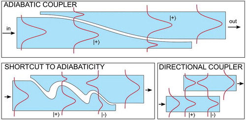
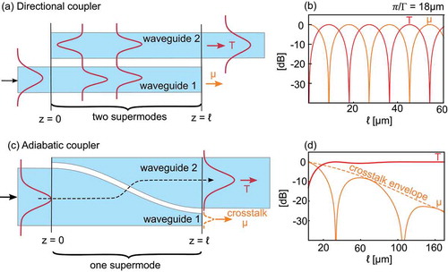
Most photonic systems require the efficient transfer of light from one waveguide into another [Citation7], so a number of different approaches have been developed to achieve it: one of these is butt coupling, in which the two waveguides are placed end-to-end [Citation8]. Such devices are by their nature very short, but the efficiency of butt-coupling can be low when the modal profiles and the propagation constants of the modes in the two waveguides are poorly matched. Another approach is the directional coupler, illustrated in ), in which the two waveguides are placed side-by-side. If the two individual waveguides have the same propagation constants and the light is coupled into an equal superposition of the two supermodes of the coupled waveguides, the light couples back and forth periodically over the length of the device ()). If the device is terminated at the correct position, all light exits through the other waveguide. Though directional couplers can be fairly short, the requirement that the waveguides have the same propagation constants, and the dependence of the coupling length on wavelength, constrain the performance in terms of fabrication tolerances and bandwidth [Citation9,Citation10].
In contrast to these two devices, adiabatic couplers, introduced into photonics by Cook [Citation11], are relatively robust devices that can have a large bandwidth [Citation6,Citation9,Citation12–18]. The type of adiabatic coupling device we are considering here is illustrated in ). We consider the two lowest supermodes of the device; approximately each supermode can be thought of as a superposition of the fundamental modes of the isolated waveguides 1 and 2. However, the device is designed such that at and
the supermodes closely match the modes of the individual waveguides: for the device in ), the fundamental supermode at
corresponds to the isolated mode of waveguide 1, whereas at
it corresponds to that of waveguide 2. For the device in the schematic, this is achieved by varying the widths of the waveguides. In a perfectly adiabatic process, light that is coupled into the fundamental supermode enters through waveguide 1, remains in the fundamental supermode, and exits via waveguide 2, ideally with 100% efficiency. A consequence of adiabaticity is that, provided that the supermodes coincide with each of the individual waveguides at
and
, the device performance is relatively insensitive to the perturbations of the device or even to the details of the device design [Citation9,Citation17].
Figure 1. (a) Schematic of a directional coupler: two supermodes, with different propagation constants, are excited at the input in waveguide 1. (b) The supermodes’ interference leads to a periodically varying output with length . (c) Schematic of an adiabatic coupler: Light is input in waveguide 1, corresponding to a supermode at
. The light remains in this mode, which at the end of the device corresponds to waveguide 2. The dashed line schematically indicates the propagation of the light. (d) As the device length
increases, the crosstalk
has discrete zeros under an envelope that decreases with
Even though adiabatic devices promise excellent performance, because of the requirement of adiabaticity they tend to be quite long–ideally they are infinitely long! It is therefore not surprising that a number of techniques have been developed that promise to minimize this length, while maintaining performance. Most of these techniques are referred to generically as Shortcuts to Adiabaticity (STA) [Citation3–6]—developed initially in the context of quantum mechanics, these have been considered for applications in optics since 2009 [Citation19]. In Section 3, we discuss these techniques and clarify their mutual relationships.
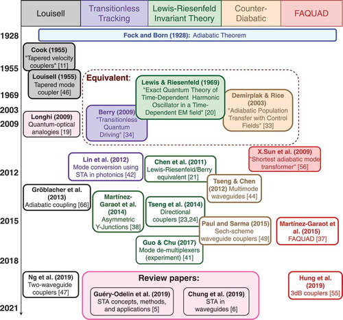
One shortcut technique we discuss in Section 3 is based on the Lewis-Riesenfeld invariant theory [Citation20–25] in which the device design is reverse-engineered to accelerate adiabatic processes, and it has been used in applications such as atomic transport [Citation26–28] and trap compression and expansions [Citation29–32]. Other STA methods include the counter-diabatic (CD) approach developed by Demirplak and Rice [Citation33] and the related transitionless tracking method of Berry [Citation34]. Starting from an initial device, they introduce an additional contribution that cancels the diabatic coupling in the original device, reducing the effect of the imperfect adiabaticity. This approach has been applied to speed up rapid adiabatic passage (RAP) in two level atoms [Citation35] and was experimentally implemented in Bose-Einstein condensates in optical lattices [Citation36]. Alternatively, in the fast quasi-adiabaticity (FAQUAD) [Citation37] technique, the adiabaticity is violated to the same extent throughout the device. We also discuss the relationships between these methods, first addressed by Chen et al [Citation21]. Although we have included a large set of references, summarises some of the main references–the foundational papers, major reviews, key references applying STA techniques in photonics–and provides a timeline.
Figure 2. Timeline with foundational papers, major reviews, and key references applying STA techniques in photonics. The figure is not intended to be exhaustive. Key references have a coloured background
While developed in the context of quantum mechanics and atomic physics, these techniques can also be applied to photonic devices when these are described using coupled mode theory (CMT). This theory enables a general, simple yet powerful description of photonic devices in which a complex physical design is expressed in terms of a reduced number of parameters. Using this framework, a coupler such as in can be described in terms of only two real functions, corresponding to the difference in propagation constant of the modes of the device (), and the strength of the coupling between the waveguides (
), each of which depends on longitudinal position, and thus
and
.
The aim of this Review is to examine the adiabatic literature in the context of waveguide couplers, and to discuss which of the techniques mentioned above can be useful in this context. Although the techniques have been applied to other devices such as junctions [Citation38,Citation39], photonic lattices [Citation40], demultiplexers [Citation41], mode converters [Citation42] and filters [Citation43], curved waveguides [Citation19], as well as multimode waveguides [Citation44] and interference splitters [Citation45], we choose to consider the coupling between two waveguides [Citation46–49] (as in ) as this is a simple nontrivial case with only two relevant modes. Therefore, the Hamiltonian that describes the interaction between these modes can be written as a matrix with position-dependent coefficients.
We consider lossless systems and we take this matrix to be real and symmetric, so that it has real Eigenvalues and orthogonal Eigenvectors. This choice deserves two comments. The first indicates a difference with quantum mechanics, where the
matrix is generally Hermitian, but in the description of the coupling between waveguides the matrix cannot have complex elements, and thus the description by a Hermitian matrix reduces to that of a real, symmetric one. The second point is that for strongly coupled waveguides, the interaction between lossless waveguides requires a real matrix that is asymmetric [Citation50,Citation51]. Such matrices are of course not Hermitian, and cannot therefore be described by the theory we are reviewing here, though we note that STA has been generalized to non-Hermitian systems [Citation52,Citation53].
The outline of this Review is as follows. In Section 2 we give a general overview of adiabatic couplers and their mathematical description. In Section 3 we review the key shortcut methods that have been most widely used and discuss their mutual relationships. In Section 4 we illustrate the use of these methods in a physically realistic geometry and compare to alternative adiabatic couplers generated by other techniques. Then, in Section 5 we compare the sensitivity of a number of different adiabatic couplers to the presence of noise in the device parameters, motivated to evaluate robustness to fabrication errors. Finally, in Section 6 we discuss our findings and conclude.
2. Adiabatic processes and FAQUAD
Waveguide couplers as in must be described by several parameters (refractive indices and dimensions of each waveguide, spacing of the waveguides, refractive index of the region between and outside the waveguides), all of which are functions of propagation length. As discussed in Section 1, in coupled mode theory only two parameters are required. In coupled mode theory the field in a waveguide is written as the product of a mode field, which depends on the transverse coordinates, and a -dependent factor describing the propagation. For an isolated waveguide this
-dependent factor is
, where
is the mode amplitude, defined such that
corresponds to the power carried by the mode. and
is the wave number of the mode. The propagation in the isolated waveguides is thus described by
.
If two waveguides and
are brought together, and allowed to interact linearly then we find
where represents the coupling between the waveguides and both
and the
are real functions of
. We note that
due to the proximity of the other waveguide. Now defining
and
, EquationEquation (1)
(1)
(1) can be rewritten as
which defines the ‘Hamiltonian’ , and where the ket
has the elements
.
In the following analysis of these equations we follow Louisell [Citation46], who, to the best of our knowledge, reported the first systematic investigation of adiabatic processes in the context of photonics. The instantaneous Eigenvalues of are
with associated Eigenvectors
corresponding to the instantaneous supermodes of the device, and where
We now write the general solution to EquationEquation (2)(2)
(2) as
; when
and
are constant, then the
vary harmonically. In general though,
and
depend on
, and the
satisfy the coupled equations [Citation46]
EquationEquations (4)(4)
(4) and (Equation5
(5)
(5) ) confirm that when
and
are constant, the
vary as
and do not couple. Variations in
and
that cause variations in
, lead to coupling of the
. In the truly adiabatic limit the derivatives on the right-hand sides in EquationEquations (5)
(5)
(5) are arbitrarily small and the equations again decouple.
Adiabatic coupling can then be understood by taking and
. If light is coupled into waveguide 1, say, at
, it is in supermode
. In an adiabatic coupler without supermode coupling, the light remains in this supermode, and therefore exits entirely through waveguide 2. Of course, for the light to remain rigorously in the same supermode throughout its propagation, the device needs to be infinitely long. All the techniques discussed in this Review correspond to strategies to minimise the device length without compromising device performance.
Although the parameters that enter the Hamiltonian are and
, they enter as the combinations
and
in the solutions. However, only variations in
cause changes in the supermodes; thus, if
and
vary at the same rate, so
is constant, then the supermodes are unchanged.
EquationEquations (5)(5)
(5) can be solved formally at various levels of approximation. Assuming that the field amplitude in the original super mode remains close to unity, the crosstalk
, that is, the fraction of the incoming power that is not coupled over at
can be written as [Citation46]
where , and
is an effective position. Note from EquationEquation (6)
(6)
(6) that
is, in essence, the Fourier transform of
, as is particularly clear when
is constant. Now recall the theorem that the Fourier transform of a function with a discontinuous
derivative, asymptotically is a power law with exponent
[Citation47,Citation54]. Applying this to EquationEquation (6)
(6)
(6) we conclude that the asymptotic behaviour of
, i.e. the behaviour as
, is determined by the inevitable discontinuities of
or any of its derivatives at
and
(assuming that
and all of its derivatives are smooth elsewhere): when the
derivative is discontinuous,
[Citation47].
) shows a typical result for the crosstalk versus device length as calculated by integrating the coupled mode EquationEquation (2)(2)
(2) . Note that the crosstalk has discrete zeros, superimposed on a monotonically decreasing envelope. Before discussing the results in ), we note that EquationEquations (5)
(5)
(5) and (Equation6
(6)
(6) ) show that the relevant quantity that determines the degree of adiabaticity involves
; in fact, the adiabaticity criterion can be written as [Citation46]
Given inequality (7), one strategy to designing a coupler is to take to be constant–this is the fast quasi-adiabatic (FAQUAD) approach, which was introduced formally by Martínez-Garaot et al. [Citation37] and applied by Hung et al. [Citation55], but was used prior to that by Sun et al. [Citation56]. From EquationEquations (5)
(5)
(5) , (Equation6
(6)
(6) ) and (Equation7
(7)
(7) ), decreasing
leads to lower crosstalk, but with a longer device. Hence, the choice is a compromise between performance and device length. Note that within the constraint of EquationEquation (7)
(7)
(7) , any
that is continuous and that has a continuous first derivative lends itself to the FAQUAD approach. Although not obvious from EquationEquation (7)
(7)
(7) , the FAQUAD procedure has the advantage that it can be applied without the need to use a coupled mode description of the device.
To illustrate the results in this section, we consider a set of couplers with parameters that can be varied systematically [Citation47]: we consider the elements of the Hamiltonian to take the values
where the normalised propagation length , with
the device length, and thus
, and
is constant. The
are polynomials which satisfy
, with
and thus
. They are most easily defined through their derivative (with respect to the argument) through [Citation47]
and thus and
, etc. As illustrated in ), at
, the lowest
derivatives of these polynomials are continuous, whereas higher ones are discontinuous. All of the designs based on EquationEquation (8)
(8)
(8) have the property that
increases smoothly from
at
to
at
. As
increases, the discontinuities at the edges become weaker, and so
needs to increase more rapidly in the central part of the coupler. Weakening the discontinuities at the edges improves the performance for large
.
Figure 3. Three different polynomial couplers at different stages of the design. (a) shows the mixing angle
along the normalised length of the device.
(a directional coupler) and
are also plotted for comparison. (b) Normalised Hamiltonian components, with coupling coefficient
(solid) and phase velocity mismatch
(dashed) versus normalised position along the device. (c) Crosstalk from solving EquationEquation (2)
(2)
(2) (solid lines) for different device lengths, keeping
constant. The crosstalk envelope (dashed line) decreases for increasing
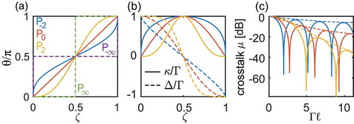
To see the drawback of increasing we consider the expression for
in more detail. For constant
and for the symmetric devices we are considering here, the crosstalk vanishes when
where . For large
,
is concentrated near
, and so the first zero occurs for large values of
, whereas for small
the first zero occurs at smaller values of
. To illustrate this, for
, the first zero in the crosstalk occurs when
, whereas for
it occurs at
, and for
at
. By comparison, for a directional coupler, for which
and thus
, the first zero occurs when
.
The couplers defined by EquationEquations (8)(8)
(8) and (Equation9
(9)
(9) ) thus illustrate the practical difficulty in choosing an ‘optimal’ design. For the polynomials with large
, the envelope (see )) decreases rapidly with
[Citation47]. Note that the crosstalk envelope represents the degree to which the mode remains in its Eigenstate during propagation. It thus indicates robustness to variations in the ideal design. For larger
, the first zero in the crosstalk appears at longer lengths. In contrast, for small
the envelope decreases slowly, but the first zero appears at shorter lengths. However, in that case the design competes with directional couplers. Thus, the criterion that is used to optimize the coupler has a strong influence on its eventual shape.
For the coupler with , the parameter
defined in EquationEquation (7)
(7)
(7) is constant, and it thus satisfies the FAQUAD condition. To compare its performance with other couplers, we extend the polynomial Ansatz from EquationEquations (8)
(8)
(8) and (Equation9
(9)
(9) ) to negative integers
. We do so by defining
, where the superscript indicates the inverse of the function (rather than its reciprocal). Thus, for all integers
, the properties listed between EquationEquations (8)
(8)
(8) and (Equation9
(9)
(9) ) are maintained. In this way, we obtain a set of couplers that range from those that are highly discontinuous at the edges, and slowly varying in the centre (
large and negative), to couplers which are smooth at the edges and rapidly varying in the centre (
large and positive), with the FAQUAD coupler as a compromise between these extremes. We discuss these further in Sections 4 and 5.
3. Shortcuts to adiabaticity: methods and relations
In this section, we describe the three STA methods that have found most widespread use [Citation57]: the invariant method of Lewis and Riesenfeld [Citation20], the work of Demirplak and Rice in counter-diabatic (CD) driving [Citation33], and Berry’s transitionless tracking (TT) algorithm [Citation34]. We first give general descriptions of each of these methods at the operator level and then explore how they can be applied to solve the particular problem of power transfer in a waveguide coupler. Furthermore, we discuss connections between these methods. To better facilitate this, notation is kept consistent between subsections where applicable. Overall, these methods provide a way to start and end in a pure state of the Hamiltonian for a given device length. We explicitly show the -dependence in all equations in this section for clarity.
3.1. Lewis-Riesenfeld invariants
The original work of Lewis and Riesenfeld [Citation20] proposes to seek a Hermitian invariant for a dynamic system driven by
satisfying
for all . Assuming the basis set is complete since the invariant arises from some observables, we can write
with the orthonormal Eigenstates and
the corresponding Eigenvalues. By considering the
-derivative of this expression in conjunction with EquationEquation (11)
(11)
(11) , Lewis and Riesenfeld [Citation20] show that
must be constant. In general, the method uses ‘reverse engineering,’ with an assumed invariant, and then derives constraints on a Hamiltonian such that EquationEquation (11)
(11)
(11) is satisfied. In doing so, states can be represented by
where the are
-independent amplitudes and
is the Lewis-Riesenfeld phase for state
. By requiring that the right hand side satisfies the dynamics in EquationEquation (2)
(2)
(2) for any choice of amplitudes, Lewis and Riesenfeld [Citation20] show that
We now turn to the particular case of a two waveguide coupler. Lai et al. [Citation58] derive a representation of the invariant for particular Hamiltonians, including the Hamiltonian in EquationEquation (2)(2)
(2) . It can be written as
with
Since and
, it satisfies the conditions of Lai et al. [Citation58], and the invariant is given by
where
Here and
are auxiliary real functions that parametrise the possible invariants. The following development closely follows that of Chen et al. [Citation21] and was later applied to waveguides by Tseng [Citation23]. Applying this procedure yields
EquationEquation (19)(19)
(19) has Eigenvalues
, with Eigenstates
Substituting EquationEquation (19)(19)
(19) into the invariance condition EquationEquation (11)
(11)
(11) yields a coupled system of differential equations
We note that the expression here may differ from those in other publications by a factor , which arises from different definitions of
. The method of Lewis-Riesenfeld is indirect, in that, once
and
are known,
and
can be found. The functions
and
are arbitrary except for their boundary conditions at
and
. At the ends of the coupler, there should be no coupling and thus
. This gives
This also ensures that , implying shared Eigenstates between
and
. From the Eigenstates in EquationEquation (20)
(20)
(20) , we observe that to start and finish in different pure states (i.e. to transfer power from one waveguide to the other) requires
or vice versa without loss of generality. EquationEquations (22)(22)
(22) and (Equation23
(23)
(23) ) are the boundary conditions that are necessary for a valid coupler that transfers power from one waveguide to the other. To validate the performance at all device lengths, Chen et al. [Citation21] chose length-invariant boundary conditions of the form
with a constant. From a dimensional analysis perspective, we observe that this is the only dependence on
that leads to identical behaviour at all device lengths. Furthermore, in the interests of keeping the coupler realistic by minimising the coupling coefficient
, Chen et al. [Citation21] chose boundary conditions on
to maximise
in EquationEquation (21)
(21)
(21)
One choice that satisfies the requirements in EquationEquations (22)(22)
(22) –(Equation25
(25)
(25) ) are third-order polynomials for
and
[Citation21].
The parameterization from to
may provide additional other benefits for waveguide couplers. Tseng [Citation23,Citation24], leveraging the work from quantum population transfer of Ruschhaupt et al. [Citation59], uses these parameters in the Lewis-Riesenfeld phase
to describe the robustness of the device to constant deviations in Hamiltonian elements. The error sensitivity as a function of invariant parameters was optimized, producing couplers that are resilient to changes in either
or
. This is discussed further in Section 5.
3.2. Counter-diabatic method
The method proposed by Demirplak and Rice [Citation33] approaches the problem from a different perspective. The central observation of this approach is that an evolving non-adiabatic Hamiltonian leads to transitions between states. These transitions arise from off-diagonal terms in the Hamiltonian, and can be countered by adding a counter-diabatic term
to the Hamiltonian. Under the dynamics of the new, ‘corrected’ Hamiltonian
the system remains in the initial Eigenstate of the non-corrected Hamiltonian [Citation57], as shown in .
Figure 4. Fractional power in the unwanted Eigenmode versus distance for a coupler designed with the counter-diabatic method. Dashed curve: power variation in the supermodes of the uncorrected Hamiltonian . Solid black curve: evolution of the corrected Hamiltonian
projected onto its Eigenstates. Red curve: same evolution, but projected onto the Eigenstates of the original Hamiltonian
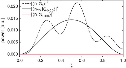
To find the appropriate counter-diabatic Hamiltonian, we transform the ket appearing in EquationEquation (2)
(2)
(2) to a basis set that evolves together with the Eigenstates of the uncorrected Hamiltonian
. These Eigenstates
satisfy
with Eigenvalues . A basis transformation must be unitary, and can generally be written as
and the evolution of the transformed system is then given by the Schrödinger EquationEquation (2)(2)
(2)
for a new Hamiltonian . To avoid transitions, this transformed Hamiltonian should be diagonal in the basis of Eigenstates
.
depends on the particular choice of
via
The first term can be made diagonal by choosing such that its row vectors are the transposed Eigenstates
, and so
The remaining off-diagonal terms can be made to vanish by choosing
For any given non-adiabatic Hamiltonian, we therefore have
where the first (diagonal) term evolves the states to match the Eigenstates at position , and
cancels out transitions resulting from the evolution. For a reference Hamiltonian
(EquationEquation (2)
(2)
(2) ) we explicitly find that EquationEquation (32)
(32)
(32) reduces to a Hamiltonian of the form
where is defined as in EquationEquation (4)
(4)
(4) . In this form, we see that the counter-diabatic Hamiltonian intuitively manifests as a correction to the coupling term
, and this correction is related to the adiabaticity criterion
(EquationEquation (7)
(7)
(7) ).
3.3. Transitionless-tracking algorithm
Berry’s transitionless tracking algorithm [Citation34] takes a similar approach to suppressing transitions between states. Instead of changing the basis of the Hamiltonian to one in which the elements are diagonal in the basis of initial states, the approach seeks to find a unitary operator that preserves adiabatic states under evolution. These adiabatic states correspond to the states traversed by the system if the change in the Hamiltonian is performed adiabatically, and are, to within a phase factor, the same as the instantaneous Eigenstates
where incorporates the integrated phase accumulation from the energy
of the state, together with the geometric phase. A unitary transformation that preserves the probability distributions of states under evolution from
to
is
The Hamiltonian that performs such a transformation can then be found. Substituting the relation into EquationEquation (2)
(2)
(2) we find
where is the original Hamiltonian and
is a correction that prevents transitions. In the particular case of a two waveguide coupler with
as in (2), the transitionless tracking algorithm yields the same correction as the counter-diabatic approach (33).
3.4. Unitary transformation enabling photonics applications
Both the counter-diabatic and transitionless tracking methods provide a correction term to the Hamiltonian. These corrections are generally complex-valued, and indeed the corrections are purely imaginary in the case of a two waveguide coupler. In the context of atomic physics and quantum state driving, their implementation is straightforward, and the imaginary component is the phase of the driving field. In optics however, the total Hamiltonian must be real in order to correspond to a passive optical device. Following Tseng [Citation48], this may be achieved through one final unitary transformation which applies a rotation in the real-imaginary plane. The rotation angle
is real and yet to be determined. Applying this unitary transformation to the Schrödinger equation, as before (see EquationEquation (28)
(28)
(28) ), we find the transformed Hamiltonian
If we apply this to the explicit form of the counter-diabatic Hamiltonian EquationEquation (33)(33)
(33) , we find that off-diagonal elements take the form
. By choosing
these elements are real, and the transformed Hamiltonian is then
Thus, for this ,
corresponds to a real matrix which can be implemented as a passive waveguide coupler. The same unitary transformation can be used in the transitionless tracking approach. Indeed, the counter-diabatic and transitionless tracking approach are closely related.
3.5. Equivalence between transitionless tracking and the counter-diabatic approach
There is a direct connection between the transitionless tracking algorithm (Section 3.3) and the counter-diabatic approaches (Section 3.2). As an overall comment, the transitionless tracking algorithm preserves adiabatic states, whereas the counter-diabatic approach preserves the Eigenstates of the instantaneous Hamiltonian. Because these are the same except for a phase factor, the two correcting Hamiltonians must be the same except along the diagonal. This can be seen directly by examining the diagonal components of
and so, comparing with Equation(36), we find
The corrected Hamiltonian from the counter-diabatic correction is therefore equal to the purely off-diagonal part of the transitionless tracking algorithm
. The two corrections therefore suppress the transitions between Eigenstates, but these Eigenstates may still undergo changes in phase. The transitionless tracking algorithm ensures that these phases evolve in the same way as those of pure adiabatic states.
Berry [Citation34] notes that the phases in EquationEquation (34)(34)
(34) can be chosen freely; doing so preserves the probability distribution amongst the states, although the states themselves evolve with a different phase than that expected from adiabatic evolution. Choosing
leads directly to the counter-diabatic approach.
3.6. Equivalence of transitionless tracking and the invariant approach
Similarly, we find that a Hamiltonian computed by the transitionless tracking method can also be generated through an invariant approach. First, consider a coupler designed by transitionless tracking. The Hamiltonian always drives states adiabatically (illustrated for a particular case in Section 4). Chen et al. [Citation21] propose that an operator of the form
satisfies the invariance condition EquationEquation (11)(11)
(11) with different choices of
. This invariant makes intuitive sense in the context of , since the basis of the original Hamiltonian
remains stationary under the dynamics of
. The simple choice
ensures that the invariant and original Hamiltonian are identical at
, giving the invariant a more grounded interpretation. In Appendix A1 we show explicitly that
satisfies EquationEquation (11)
(11)
(11) . The result also demonstrates that the choice of Eigenvalues of the invariant
hold no great significance in terms of the final coupler produced. In the opposite direction, we can ask if, for every Hermitian invariant
satisfying EquationEquation (11)
(11)
(11) , there exists a Hamiltonian
, which, when applying the transitionless tracking method, gives the same
as the invariant method. Chen et al. [Citation21] propose that the choice
accomplishes this, where again represents the Eigenvalues of the invariant. The Lewis-Riesenfeld phase
can be calculated from the invariant approach EquationEquation (14)
(14)
(14) , and it replaces the Berry phase
.
Unitary transforms, however, result in a need to modify this: if is real when produced by the transitionless tracking algorithm, and
from EquationEquation (41)
(41)
(41) is real since
are real (from a real
), then EquationEquation (11)
(11)
(11) is not satisfied since one term is real and the other imaginary. Hence, we propose a different invariant
with as some unitary transform and
is the basis state for the original Hamiltonian
. In Appendix A2 we explicitly verify that this satisfies Equation (11) with
from EquationEquation (37)
(37)
(37) . The result is applicable to any unitary transformation
, including
in Section 3.4. It is possible to generate a plot similar to for the unitary transformed dynamics, where projecting the state vector
onto the transformed basis
shows zero changes in mode power. Again, this makes intuitive sense—stationary states should become the basis of the invariant. In the context of waveguide couplers, however, this basis not only no longer exists but also it is unphysical since
. In the other direction of equivalence, one can obtain an initial Hamiltonian
by transforming
to
in EquationEquation (42)
(42)
(42) .
Thus, all three of the presented methods are equivalent, at the operator level, even when constraining the Hamiltonian through unitary transformation to produce physical waveguides.
4. Adiabatic processes in realistic waveguides
So far, we have reviewed adiabatic processes on the basis of coupled mode theory (CMT) using EquationEquation (2)(2)
(2) as a starting point, with the parameters
and
characterizing the coupler and its performance (e.g. the crosstalk
). While this approach provides a wealth of information on coupler properties, the conceptual link to physical devices is less obvious. In this section, we review pathways and implications of implementing adiabatic couplers in practice. The modes and full propagation properties of arbitrary geometries can be calculated with commercial numerical mode solvers (e.g. COMSOL, Lumerical, etc.), and can be used as a tool for evaluating the coupled mode formalism. In this Review, we show results generated by finite element method (FEM) calculations implemented in COMSOL.
The link between coupled mode theory and physical waveguides can be approached in two ways: (i) a physical embodiment of a coupler can be used to calculate and
to solve EquationEquation (2)
(2)
(2) and predict coupler properties; (ii) vice versa, a desired distribution of
and
targeting certain device characteristics can be given a physical embodiment. We now review both cases, comparing the crosstalk predicted by various methods with full finite element calculations. Section 4.1 reviews the properties of a previously reported two-waveguide adiabatic coupler [Citation47] as an illustrative example and as starting point for the subsequent discussion. Section 4.2 then presents typical approaches for applying two different protocols to this example physical system: the counter-diabatic correction of Sec. 3.4 in Section 4.2.1, and the FAQUAD approach from Sec. 2 in Section 4.2.2. Section 4.2.3 concludes with a comparison of the physical embodiment of the
polynomials of with a reasonable choice of
.
Below we discuss the properties of example couplers and their scaled counterparts. The scaled device is related to the original device by stretching or compressing without other modifications. As we showed in Section 3.2 the CD correction guarantees vanishing crosstalk but requires a different correction for every choice of length. In the spirit of analyzing a device’s crosstalk envelope however, below we apply the CD correction once for a single length, and present how the crosstalk varies as the resulting device is scaled.
Figure 5. Example adiabatic device from Ng et al. [Citation47]. (a) Finite element calculation and definition of physical parameters ,
, and
. (b) Resulting effective index of the isolated and coupled waveguides. (c) Computed
,
and
, and (d)
. (e) Resulting
(dashed line:
.) (f) Crosstalk according to Louisell (EquationEquation (6)
(6)
(6) ), coupled mode theory (CMT, solution of EquationEquation (2)
(2)
(2) ), and finite element calculations
![Figure 5. Example adiabatic device from Ng et al. [Citation47]. (a) Finite element calculation and definition of physical parameters w1, w2, and s. (b) Resulting effective index of the isolated and coupled waveguides. (c) Computed Δ, Γ and κ, and (d) θ. (e) Resulting η (dashed line: η=1.) (f) Crosstalk according to Louisell (EquationEquation (6)(6) μ=14∫0ℓdθdze−2i∫0zΓ(z′)dz′dz2=14∫0ρ(ℓ)dθdρe−2iρdρ2,(6) ), coupled mode theory (CMT, solution of EquationEquation (2)(2) ddz|G⟩=−iΔκκ−Δ|G⟩≡−iH|G⟩,(2) ), and finite element calculations](/cms/asset/7236a3f0-4d2d-4594-b3f6-8975482432d6/tapx_a_1894978_f0005_oc.jpg)
4.1. Parabolic coupler
As discussed in Section 2, the coupled mode formalism is agnostic to the waveguides’ physical embodiment: two parameters and
describe infinitely many materials, wavelengths and geometries, which in a chip-based, two-waveguide scenario can include the width and height of each waveguide, and their relative separations. In order to simplify the discussion and to reduce the physical parameter space, we consider a previously reported example [Citation47], consisting of two 1D waveguides (WGs) at
, formed by silica (
[Citation60]) in air, under transverse magnetic (TM) polarization, as shown in ). In this case, the only relevant physical parameters are the widths of WG1 and WG2 (
and
, respectively), and their edge-to-edge spacing
. This representative device is a judicious embodiment of the ) schematic; the width of the input WG1 decreases linearly from 700 nm to 300 nm, and the width of WG2 increases from 300 nm to 700 nm, so that
is approximately a straight line with negative slope with
at the centre of the device; the separation varies parabolically such that
at the edges
in the centre, ensuring that the coupling coefficient
vanishes at the edges and peaks in the centre. Combining these characteristics broadly satisfies typical requirements for
and
of an adiabatic coupler [Citation46]. The white curves in ) give a geometrical outline of the coupler. The colors show the Poynting vector for the particular example of
, and confirm that most of the light couples between the waveguides in the region where they approach each other closely.
) shows the calculated effective index of the Eigenmodes of the full two-waveguide system versus position. The dashed lines in ) show the corresponding effective index
of the modes of the isolated waveguides. The parameters in ) yield the parameters
,
and
, shown in ) which are obtained directly from
These can be used to obtain from EquationEquation (4)
(4)
(4) (see )). Subsequently,
can be obtained from EquationEquation (7)
(7)
(7) , shown in ) for different device lengths
. Recall that the adiabatic condition is
: this condition is satisfied at all points along the device for
(green curve in )), and is satisfied near the edges when
(blue curve in )). Finally,
represents an intermediate case where
along the entire device.
Knowing both physical parameters and coupled-mode parameters, the crosstalk can be calculated in three different ways. The results are summarized in ), which shows
versus device length
. The blue curve gives the result of integrating Louisell’s result (EquationEquation (6)
(6)
(6) ) [Citation46], and the orange curve gives the result obtained by numerically integrating the coupled mode equations (EquationEquation (2)
(2)
(2) ). The agreement between these curves shows that EquationEquation (6)
(6)
(6) is accurate for the parameters in this example, whereby the largest discrepancy occurs at short lengths where EquationEquation (6)
(6)
(6) is not expected to be valid [Citation46]. The black curve shows
obtained from a full two-dimensional finite element calculation of the physical system in ), showing excellent agreement with the previous methods, confirming the validity of all methods to describe this physical system.
4.2. Application of shortcuts and protocols
With knowledge of all important parameters for our chosen system, we are now in a position to apply the procedures presented in Section 3, and review their impact on both performance and physical embodiment of the device. Note that there are still many combinations of ,
, and
that lead to the same
and
, even keeping the material and wavelength constant as we do here. Therefore, when choosing the physical representation for a given set of parameters, we fix the bottom waveguide in its current configuration (i.e.
decreases linearly from 700 nm to 300 nm), and modify the edge-to-edge separation
and top waveguide width
to yield a desired
and
at each
. For a fixed
, there is a unique value of
that provides a desired
, which describes the uncoupled waveguides. Once this is known, there is a unique value of
that yields the desired
. This approach is valid for waveguides that are not too strongly coupled, such that the off-diagonal- terms in EquationEquation (2)
(2)
(2) are equal [Citation61,Citation62]. Our choice significantly reduces the potential parameter space, but is representative of typical experimental approaches [Citation63], and enables a direct comparison between the physical embodiment and coupled mode theory, providing insight into the applicability of this formalism for practical applications.
4.2.1. Counter-diabatic correction
Since the counter-diabatic, transitionless tracking and invariant approaches are all equivalent, we may consider the performance of a counter-diabatic device to be indicative of all three. The counter-diabatic correction for a device of length is obtained by replacing
in EquationEquation (2)
(2)
(2) with
in EquationEquation (38)
(38)
(38) , as outlined in Ref [Citation48]. Since
, it follows that
is different for every choice of
. As an illustrative example, we apply the CD correction to the waveguide system of via the parameters in ) for a device of length
. The results are shown in ): relative to the original structure, the CD protocol induces a strong modulation of the corrected
and
in the central region, which overall increases
. The parameters of the physical embodiment, given our constraints on the bottom waveguide, are shown in ):
and
vary in the centre, leading to an increase in the coupling constant
in the center of the device. The strongly oscillating
(blue curve in )), leads to
for our value of
, indicating that this CD-corrected device is less adiabatic than the original. Calculating the crosstalk
using different methods, shown in ), reveals that while this design gives the desired low crosstalk
for this specific
(black arrow in )), the scaling of this profile for increasing lengths leads to an overall larger envelope than the original structure. Finally, while the finite element calculations of the physical device faithfully reproduce the overall crosstalk envelope, shown in ), as well as the salient features predicted by EquationEquations (2)
(2)
(2) and (Equation6
(6)
(6) ), the physical device has a larger crosstalk at the design length
than EquationEquation (6)
(6)
(6) predicts, as a result of the large curvature of the top waveguide over wavelength-scale distances, leading to the leaking of radiation into the bottom waveguide.
Figure 6. CD (left) and FAQUAD (right) corrections to the device in . (a) ,
and
obtained by applying the CD correction (EquationEquation (38)
(38)
(38) ) to the parameters in ),(d) for
, and (b) resulting physical parameters defined in ). (c) Comparison of
(left axis) and
. (d) Resulting crosstalk according to Louisell (EquationEquation (6)
(6)
(6) , blue), coupled mode theory (solution of EquationEquation (2)
(2)
(2) , orange), and FEM calculations (black). (e) obtained by applying the FAQUAD protocol to the parameters in ), and (d), and (f), resulting physical parameters as defined in Fig. 5(a). (g) Comparison of
and
at
:
is constant as required. (h) Resulting crosstalk according to Louisell (EquationEquation (6)
(6)
(6) , dashed blue), coupled mode theory (CMT, solution of EquationEquation (2)
(2)
(2) , orange), and FEM calculations (black)
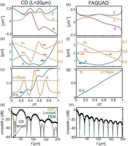
4.2.2. FAQUAD correction
The fast quasi-adiabatic (FAQUAD) correction [Citation64] is a design protocol which aims at homogeneously distributing adiabaticity during propagation, which means that in EquationEquation (7)
(7)
(7) is constant. While there are many ways to achieve this, a typical approach [Citation64] integrates EquationEquation (7)
(7)
(7) using
and
of a chosen device. This leads to a transformation of
: intuitively, EquationEquation (7)
(7)
(7) informs the degree by which
should be stretched or compressed along the device so as to distribute adiabaticity equally, thereby avoiding scenarios wherein the adiabatic condition is satisfied only for certain regions. This is especially important for short devices—see, for example, the blue curve in ), which shows that for a short device length EquationEquation (7)
(7)
(7) is satisfied at the edges but not in the centre.
The parameters obtained by the FAQUAD correction to the device in are shown in ). The corresponding physical device parameters, shown in ), are consistent with the expectations from the adiabaticity criterion at short lengths: at the edges, the device already satisfies the adiabaticity criterion so that and
vary faster, whereas in the centre these parameters vary more slowly. The resulting values of
and
are shown in ):
is flat and constant, as required by the FAQUAD condition, whereas
approaches a straight line. The calculated crosstalk for this device using different methods is shown in ). Note that the crosstalk envelope scales as
, consistent with earlier results for
[Citation47,Citation56]. However, this scales less rapidly than for the original coupler, which follows
()). This exemplifies the scenario whereby the FAQUAD procedure pushes the first zero to a shorter device length, at the expense of increasing the crosstalk envelope.
Figure 7. Polynomial approach with . (a)
,
and
obtained from EquationEquation (9)
(9)
(9) for
. (b) Retrieved physical parameters defined in ). (c) Comparison of
and
at
. (d) Resulting crosstalk according to Louisell (EquationEquation (6)
(6)
(6) , blue), coupled mode theory (solution of EquationEquation (2)
(2)
(2) , orange), and FEM calculations (black). (e)
,
and
obtained from EquationEquation (9)
(9)
(9) for
. (f) Retrieved physical parameters defined in ). (g) Comparison of
and
at
. (h) Resulting crosstalk according to Louisell (EquationEquation (6)
(6)
(6) , blue), coupled mode theory (CMT, solution of EquationEquation (2)
(2)
(2) , orange), and FEM calculations (black)
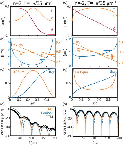
4.2.3. Polynomial profiles
An alternative approach for adiabatic coupler design relies on appropriately defining the and
profiles at constant
, via polynomials of increasing order
(EquationEquation (9)
(9)
(9) ). We have already discussed how increasing
leads to a reduced device crosstalk envelope as
for
and when
[Citation47]. We now give
and
a physical embodiment for
. Note that, in contrast to counter-diabatic/transitionless tracking and FAQUAD, this protocol relies on designing a device on the basis of pre-determined coupled-mode parameters, rather than correcting an initial profile. In order to implement the desired structure, the only new choice is that of the parameter
, where
is a characteristic beat length [Citation46]. We choose
as shown in the blue curve of ), which is comparable to the minimum
of our example device (blue curve in )). The resulting values of
and
when
are shown in the orange and red curves of ), respectively. With a linearly decreasing bottom waveguide width (dashed orange line in )), the edge-to-edge separation follows again a quasi-parabolic shape (blue line in )); in contrast to all cases considered so far however, the width of top waveguide
also decreases linearly near the edges (orange line in )), with a cross-over point in the centre. As earlier, this corresponds to increasing and then decreasing the coupling between waveguides (as per
) by first bringing them together and further apart, while changing their relative widths gradually near the edges and rapidly in the centre near the cross-over point (following
). The resulting
, shown in (blue line), follows the expected functional form (see also ). The corresponding value of
calculated for
is shown in (orange line) and suggests that, strictly speaking, the adiabatic condition of EquationEquation (7)
(7)
(7) is only weakly satisfied since
. However, as shown in ), this device exhibits the most rapid drop in crosstalk (
), despite having the smallest average
across its length.
Finally, we consider the equivalent case where , exemplified by the parameters in ). Relative to
, this device approaches the structures of a directional-coupler: the inter-waveguide separation varies slowly in the centre, with rapid changes only at the edges (blue curve in )); the top waveguide width
varies weakly with length (solid orange curve in )), and although
for much of the device ()), the envelope decreases slowly, with periodic variations that are reminiscent of a directional coupler – compare with ).
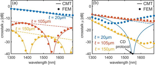
Figure 8. Bandwidth calculations. (a) CMT (solid lines) and FEM calculations (circles) for the crosstalk as a function of wavelength for the physical device shown in ), at (blue),
(red) and
(yellow). (b) Equivalent calculations for the device with the physical profile shown in ), where the CD protocol has been applied at
and
. Dashed lines indicate the crosstalk envelope
4.2.4. Bandwidth
One key advantage of adiabatic couplers with respect to directional couplers is their larger bandwidth which, as illustrated in , is due to slow changes in a single mode’s spatial profile, rather than interference effects between multiple modes. In practice however, the modes supported by an adiabatic device weakly couple as its spatial profile changes, so that the drop in the crosstalk envelope for increasing is accompanied by periodic local minima due to interference effects (see, for example, )).
Similar behaviour occurs in the wavelength dependence. ) shows the crosstalk versus wavelength for the adiabatic device of ) for three different representative lengths, and ignoring material dispersion. We consider , which, respectively, correspond to a short device, and a local minimum/maximum of the crosstalk envelope at
(see also ). Increasing
leads to an overall decrease in the bandwidth envelope (dashed line), but with periodic local minima due to interference. Note in particular the good agreement between FEM calculations (dots) and the CMT approach (solid lines), obtained by numerically solving EquationEquation (2)
(2)
(2) after separately calculating
,
and
at every wavelength via EquationEquation (44)
(44)
(44) .
We next analyze the bandwidth for the device with the physical profile shown in ), which was obtained by applying the CD protocol to the device of ) at and
. In this case, CMT calculations show perfect transfer where the device protocol was applied, with an increase in
at other wavelengths. Nevertheless, the crosstalk envelope at
is reduced with respect to the original device by approximately 6 dB. This conclusion is consistent with recent experiments [Citation41,Citation55,Citation65] reporting that STA devices can achieve good bandwidth at relatively shorter lengths. Physically scaling this device to longer lengths, however, shows the same overall increase in crosstalk envelope observed when comparing ). Note the good agreement between FEM and CMT calculations, except for the shortest device where the CD protocol was applied, as a result of radiation leakage into the bottom waveguide due to the sharp curvature of the top waveguide at short lengths. Although this might be improved by other choices of
,
and
which produce the same
,
and
, this example suggests that there are some difficulties in translating the extreme performance of CD devices at extremely short lengths into physically realistic devices.
Finally, the analysis of the dependence of crosstalk on and
highlights the importance of considering the crosstalk envelope, and more generally the envelope of any parameter of interest, since it provides a broader view of the robustness of the device to interference effects.
5. Noise sensitivity
Adiabatic couplers are expected to be less sensitive to fabrication errors than directional couplers [Citation11,Citation66,Citation67]. Estimating the performance of a coupler in the presence of fabrication errors is difficult as detailed knowledge of the fabrication errors is required. Furthermore, the connection between these physical errors and coupled mode theory is non-trivial (see Section 4). However, the frequency of a noise source is conserved between the two descriptions. We therefore evaluate the device performance by simulating noise on ,
and determining the crosstalk by numerically solving EquationEquation (2)
(2)
(2) . We choose devices all with the same length
that exhibit perfect coupling in the absence of noise. We then apply Gaussian noise characterized by a variance
, such that
is proportional to the average of
in each device consistent with
. This approach, which is agnostic to a particular type of fabrication error, allows us to compare the properties of different types of designs discussed in Section 4 in including one that was optimized for insensitivity to noise [Citation23].
We take the noise to be Gaussian, characterized by a variance and with an exponentially decaying correlation with characteristic length
, which can be much smaller, similar or much longer than the coupler length
. Our implementation follows that of Farahmand and de Sterke [Citation68], according to whom the deviation
(where
represents either
or
) at
can be found from that at
, via the Gaussian distribution
where . Steps are taken in
in intervals of
or
, whichever is smaller. This model is Gaussian to all orders, with
scaling the standard deviation
for each step. Since shorter couplers are in general more sensitive and have higher
, we choose a relative error
with respect to the average value of
(a) and (f) illustrate the resulting variation of parameters and
from the ideal along the length of the device for two different correlation lengths. Note that
has been exaggerated (
=10%) to clearly show how the correlation length affects the noise.
Figure 9. Top row solid curves: exaggerated noise model with , when applied to
(orange) and
(blue) compared to the ideal designs (dashed). (a) correlation length
and (f)
. Other figures give crosstalk
versus correlation length with
. All couplers have length
, and, without noise, they are ideal and have no crosstalk. Noise is applied to
only (blue),
only (orange) and both (yellow) for
realisations and averaged. Error bars indicate the standard error of the mean. Crosses on the right are the result as
, calulated using EquationEquation (47)
(47)
(47) . The noise floor is approximately
. Left column: STA designs using Lewis-Riesenfeld invariants with third-order polynomial for
and
[Citation21], with different boundary conditions (EquationEquation (24)
(24)
(24) ): (b)
; (c)
; and (d)
. (e)
-robust coupler [Citation23], designed to be robust to variations in
. Right column: conventional couplers: (g) directional coupler; polynomial designs (h)
; (i)
; and (j)
![Figure 9. Top row solid curves: exaggerated noise model with ε=10%, when applied to Δ (orange) and κ (blue) compared to the ideal designs (dashed). (a) correlation length ℓc=ℓ/50 and (f) ℓc=2ℓ. Other figures give crosstalk μ versus correlation length with ε=1%. All couplers have length ℓ=1, and, without noise, they are ideal and have no crosstalk. Noise is applied to κ only (blue), Δ only (orange) and both (yellow) for N=100 realisations and averaged. Error bars indicate the standard error of the mean. Crosses on the right are the result as ℓc→∞, calulated using EquationEquation (47)(47) μ(Lc→∞)=14πσ2∫−∞∞∫−∞∞exp−(δκ)2+(δΔ)22σ2μ(Δ+δΔ,κ+δκ)d(δκ)d(δΔ),(47) . The noise floor is approximately 10−8. Left column: STA designs using Lewis-Riesenfeld invariants with third-order polynomial for γLR and βLR [Citation21], with different boundary conditions (EquationEquation (24)(24) dβLRdzz=0=−dβLRdzz=ℓ=Cℓ,(24) ): (b) C=π/2; (c) C=π; and (d) C=3π/2. (e) Δ-robust coupler [Citation23], designed to be robust to variations in Δ. Right column: conventional couplers: (g) directional coupler; polynomial designs (h) P−2; (i) P0; and (j) P2](/cms/asset/1e1f0426-f571-4f5e-a338-a8009454c9f9/tapx_a_1894978_f0009_oc.jpg)
(b)–(e) and (g)–(f) give the results of our noise analysis for eight different couplers. It shows the crosstalk for noise on alone (blue),
alone (orange) and on both
and
(yellow) by numerically integrating EquationEquation (2)
(2)
(2) with the modified parameters. For each coupler, we use the same noise profiles, but scaled appropriately to match EquationEquation (46)
(46)
(46) . This avoids random variations between couplers. We generate
realisations of the random process and show the average, as well as the standard error of the mean as the standard deviation of the sample divided by
. When
, the error becomes a Gaussian distributed constant offset over the length of the device, and the effects of the crosstalk can then be computed directly, without averaging, via
for the case of noise on both and
. Here
is the crosstalk from numerically integrating EquationEquation (2)
(2)
(2) . Similarly, a single integral is evaluated for the case of noise on one Hamiltonian element at a time. The results of such calculations are indicated by crosses in .
We select a wide range of coupler designs. The STA couplers selected are taken to be of the invariant approach, and are third-order polynomial designs of and
[Citation21]. Boundary conditions EquationEquations (22)
(22)
(22) –(Equation25
(25)
(25) ) are imposed, with coefficient
()–(d)). Recall that this is equivalent to both the counter-diabatic and transitionless tracking methods, hence demonstrating the behaviour of typical STA couplers. The fourth STA coupler is that of Tseng’s, which has been optimized to be insensitive to
noise [Citation23] ()) using a perturbation analysis. We compare the performance of these couplers to other designs: a standard directional coupler ()), and those designed by polynomials
()–(j)). All couplers are designed to produce perfect power transfer at
and without noise, but scaling
produces the same results at different device lengths. Unsurprisingly, perhaps, the effect of noise on both
and
is approximately the superposition of the crosstalk with noise on each individually.
Overall, couplers designed by STA methods (left column) tend to have lower crosstalk at longer correlation lengths, while conventional couplers (right column) perform better at shorter correlation lengths. However, their performance at short correlation lengths does not differ markedly from the other designs. Fabrication errors tend to have short correlation lengths relative to the length of typical couplers. Poulton et al. report tens of nanometers [Citation69]. At such scales, there is no significant gain over a simple directional coupler, which can be further optimized for robustness [Citation70]. The primary motivation behind adiabatic couplers is that they are inherently more robust to variations in device parameters, but it appears that this advantage is lost upon the application of STA–the device in ) has poor performance at all correlation lengths with noise applied to both and
.
6. Discussion and conclusions
The efficient coupling of light between two waveguides is an important function in photonics, and many approaches have been brought to bear on it. While in this Review we have discussed adiabatic couplers, they are related to directional couplers. We have distinguished two broad measures to judge the response. The first of these is the position of the first zero of the crosstalk, indicating the shortest device that can provide perfect coupling. However, such devices would be expected to be sensitive to fabrication errors and other non-idealities. The second measure is the decay rate of the crosstalk envelope–if this envelope decays rapidly with length then the crosstalk might be expected to be robust against perturbations. These two criteria seem to be mutually exclusive and in fact we can distinguish a continuum of couplers for which the directional coupler and high-order polynomial couplers (with ) are the extreme cases. These polynomial couplers with
are characterized by a high degree of smoothness of the parameters at the two edges of the device and rapidly varying parameters in the centre. Such devices have rapidly decreasing envelopes scaling with
, but the first zero requires a fairly long device. In contrast, polynomial couplers with negative
have more severe discontinuities at the edges of the device, but vary more slowly in the centre. They have a slowly decreasing crosstalk envelope, but the first zero in the crosstalk appears at short device lengths. The directional coupler is an extreme example of this–its crosstalk envelope is periodic and does not decrease at all, but the first zero occurs as early as
. The FAQUAD approach seems to be a compromise between these two. In a recent development, Wu et al. [Citation71] describe a generalization of the concept of FAQUAD, though this intriguing proposal needs more thorough investigation.
The discussion in the previous paragraph does not explicitly include the STA-based design procedures. In our experience, the practical outcomes of these procedures are coupler designs which have zero crosstalk at a particular, designated length. However, such designs do not address the envelope of the crosstalk, nor is the length where the crosstalk vanishes necessarily particularly short. The advantage, then, perhaps lies in other aspects of the design? One of the advantages of STA-based designs is the improvement in bandwidth, as discussed in Section 4.2.4. The sensitivity to fabrication errors is discussed below.
Ideally, one would model the sensitivity of the design to the most likely type of fabrication errors. Such questions have been considered at a general level in previous papers [Citation23,Citation59], but these were carried over from quantum mechanics, where a physical parameter, for example the frequency offset of a laser, is directly related to the elements of the Hamiltonian. In contrast, in photonics this link is more indirect–an error in the width of a waveguide, for example, affects both and
. It changes
since it changes the propagation constant of the waveguide mode; it changes
since the evanescent field of that mode changes, and hence the overlap with the waveguide. In addition to this, these errors depend on the particular fabrication method that is used, and it can even depend on the particular piece of equipment. We therefore limited our analysis to investigating the noise model in Section 5 and considered the sensitivity to noise with various correlation lengths. shows the results of a set of such calculations, with a STA-designed coupler on the left and other couplers on the right. Our conclusion is that while neither of the two classes of couplers is obviously superior to the other over the entire range of correlation lengths, which covers four orders of magnitude, some of the devices perform excellently in more limited contexts. In particular, Tseng’s design in ), which is designed to be insensitive to noise in
[Citation23], outperforms all other devices for
-noise with long correlation lengths. Thus, this design would lead to excellent devices for which this is the predominant fabrication error. However, as discussed above, the relationship between the fabrication errors and device parameters is complicated. The challenge, then, would be to generalize these very powerful methods to other frequency regimes and to correlated errors in
and
.
In conclusion, while the STA-techniques provide a beautiful and consistent mathematical framework, based on the analysis we have carried out, the case for its use in the design of waveguide couplers is not clear. We surmise that this is because, even though the description of such devices can be cast in a Hamiltonian framework, the nature of likely errors is indirect and complicated and may be specific to particular fabrication methods. Considering conventional design methods, the polynomial approach that we earlier introduced [Citation47], augmented here with negative orders, provides a systematic way to balance the need for a rapidly decreasing envelope ( large and positive) with the need for zero crosstalk for a short device, with FAQUAD devices in between as a compromise. These couplers are characterized by having constant
; generalization to couplers with varying
can be considered, but there seems to be no overwhelming advantage of one over the other. In practice, then, the design chosen is likely to depend on the particular device requirements. As a final comment we note that while we only considered two-mode couplers, STA-based techniques have been applied to a large number of photonic devices including multimode devices [Citation39,Citation44]. Although the conclusion reached here may not apply to all of these, we speculate that the crosstalk envelope, that we introduced here as a performance measure, carries over to other devices since they are a consequence of modal interference effects.
Disclosure statement
No potential conflict of interest was reported by the authors.
Additional information
Funding
References
- Born M, Fock V. Beweis des Adiabatensatzes. Zeitschrift für Physik. 1928;51:165–37.
- Vitanov NV, Halfmann T, Shore BW, et al. Laser-induced population transfer by adiabatic passage techniques. Annu Rev Phys Chem. 2001;52:763––809.
- Torrontegui E, Ibáñez S, Martínez-Garaot S, et al. Advances in atomic, molecular, and optical physics, Vol. 62, chap. 2 – Shortcuts to Adiabaticity. Cambridge, MA: Academic Press, 2013; pp.117–169.
- Del Campo A, Kim K. Focus on shortcuts to adiabaticity. New J Phys. 2019;21:050201.
- Guéry-Odelin D, Ruschhaupt A, Kiely A, et al. Shortcuts to adiabaticity: concepts, methods, and applications. Rev Mod Phys. 2019;91:045001.
- Chung H-C, Martínez-Garaot S, Chen X, et al. Shortcuts to adiabaticity in optical waveguides. EPL (Europhysics Letters). 2019;127:34001.
- Marchetti R, Lacava C, Carroll L, et al. Coupling strategies for silicon photonics integrated chips. Photon Res. 2019;7:201–239.
- Hunsperger RG, Yariv A, Lee A. Parallel end-butt coupling for optical integrated circuits. Appl Opt. 1977;16:1026–1032.
- Solehmainen K, Kapulainen M, Harjanne M, et al. Adiabatic and multimode interference couplers on silicon-on-insulator. IEEE Photonics Technol Lett. 2006;18:2287–2289.
- Xu D-X, Densmore A, Waldron P, et al. High bandwidth SOI photonic wire ring resonators using MMI couplers. Opt Express. 2007;15:3149–3155.
- Cook JS. Tapered velocity couplers. Bell Syst Tech J. 1955;34:807–822.
- Riesen N, Love JD. Tapered velocity mode-selective couplers. J Lightwave Technol. 2013;31:2163–2169.
- Riesen N, Love JD. Ultra-broadband tapered mode-selective couplers for few-mode optical fiber networks. IEEE Photonics Technol Lett. 2013;25:2501–2504.
- Ramadan TA, Scarmozzino R, Osgood RM. Adiabatic couplers: design rules and optimization. J Lightwave Technol. 1998;16:277–283.
- Oukraou H, Vittadello L, Coda V, et al. Control of adiabatic light transfer in coupled waveguides with longitudinally varying detuning. Phys Rev A. 2017;95:023811.
- Chang Y-C, Roberts SP, Stern B, et al., Resonance-free light recycling (2017).
- Hassan K, Durantin C, Hugues V, et al. Robust silicon-on-insulator adiabatic splitter optimized by metamodeling. Appl Opt. 2017;56:2047–2052.
- Xing J, Xiong K, Xu H, et al. Silicon-on-insulator-based adiabatic splitter with simultaneous tapering of velocity and coupling. Opt Lett. 2013;38:2221–2223.
- Longhi S. Quantum-optical analogies using photonic structures. Laser Photon Rev. 2009;3:243–261.
- Lewis HR, Riesenfeld WB. An exact quantum theory of the time-dependent harmonic oscillator and of a charged particle in a time‐dependent electromagnetic field. J Math Phys. 1969;10:1458–1473.
- Chen X, Torrontegui E, Muga JG. Lewis-Riesenfeld invariants and transitionless quantum driving. Phys Rev A. 2011;83:062116.
- Chen X, Wen R-D, Tseng S-Y. Analysis of optical directional couplers using shortcuts to adiabaticity. Opt Express. 2016;24:18322–18331.
- Tseng S-Y, Wen R-D, Chiu Y-F, et al. Short and robust directional couplers designed by shortcuts to adiabaticity. Opt Express. 2014;22:18849–18859.
- Tseng S-Y. Robust coupled-waveguide devices using shortcuts to adiabaticity. Opt Lett. 2014;39:6600–6603.
- Ho C-P, Tseng S-Y. Optimization of adiabaticity in coupled-waveguide devices using shortcuts to adiabaticity. Opt Lett. 2015;40:4831–4834.
- Torrontegui E, Ibáñez S, Chen X, et al. Fast atomic transport without vibrational heating. Phys Rev A. 2011;83:013415.
- Torrontegui E, Chen X, Modugno M, et al. Fast transport of Bose–Einstein condensates. New J Phys. 2012;14:013031.
- Chen X, Torrontegui E, Stefanatos D, et al. Optimal trajectories for efficient atomic transport without final excitation. Phys Rev A. 2011;84:043415.
- Muga JG, Chen X, Ruschhaupt A, et al. Frictionless dynamics of Bose–Einstein condensates under fast trap variations. J Phys B: At Mol Opt Phys. 2009;42:241001.
- Chen X, Muga JG. Transient energy excitation in shortcuts to adiabaticity for the time-dependent harmonic oscillator. Phys Rev A. 2010;82:053403.
- Stefanatos D, Ruths J, Li J-S. Frictionless atom cooling in harmonic traps: a time-optimal approach. Phys Rev A. 2010;82:063422.
- Schaff J-F, Song X-L, Vignolo P, et al. Fast optimal transition between two equilibrium states. Phys Rev A. 2010;82:033430.
- Demirplak M, Rice SA. Adiabatic population transfer with control fields. J Phys Chem A. 2003;107:9937–9945.
- Berry MV. Transitionless quantum driving. J Phys A Math Theor. 2009;42:365303.
- Chen X, Lizuain I, Ruschhaupt A, et al. Shortcut to adiabatic passage in two- and three-level atoms. Phys Rev Lett. 2010;105:123003.
- Bason MG, Viteau M, Malossi N, et al. High-fidelity quantum driving. Nat Phys. 2011;8:147–152.
- Martínez-Garaot S, Ruschhaupt A, Gillet J, et al. Fast quasiadiabatic dynamics. Phys Rev A. 2015;92:043406.
- Martínez-Garaot S, Tseng S-Y, Muga JG. Compact and high conversion efficiency mode-sorting asymmetric-Y junction using shortcuts to adiabaticity. Opt Lett. 2014;39:2306–2309.
- Valle GD, Perozziello G, Longhi S. Shortcut to adiabaticity in full-wave optics for ultra-compact waveguide junctions. J Opt 2016;18:09LT03.
- Stefanatos D. Design of a photonic lattice using shortcuts to adiabaticity. Phys Rev A. 2014;90:023811.
- Guo D, Chu T. Silicon mode (de)multiplexers with parameters optimized using shortcuts to adiabaticity. Opt Express. 2017;25:9160–9170.
- Lin T-Y, Hsiao F-C, Jhang Y-W, et al. Mode conversion using optical analogy of shortcut to adiabatic passage in engineered multimode waveguides. Opt Express. 2012;20:24085–24092.
- Della Valle G. Ultracompact low-pass modal filters based on shortcuts to adiabaticity. Phys Rev A. 2018;98:053861.
- Tseng S-Y, Chen X. Engineering of fast mode conversion in multimode waveguides. Opt Lett. 2012;37:5118–5120.
- Zanzi A, Brimont A, Griol A, et al. Compact and low-loss asymmetrical multimode interference splitter for power monitoring applications. Opt Lett. 2016;41:227–229.
- Louisell WH. Analysis of the single tapered mode coupler. Bell Syst Tech J. 1955;34:853–870.
- Ng V, Tuniz A, Dawes JM, et al. Insights from a systematic study of crosstalk in adiabatic couplers. OSA Contin. 2019;2:629–639.
- Tseng S-Y. Counterdiabatic mode-evolution based coupled-waveguide devices. Opt Express. 2013;21:21224–21235.
- Paul K, Sarma AK. Shortcut to adiabatic passage in a waveguide coupler with a complex-hyperbolic-secant scheme. Phys Rev A. 2015;91:053406.
- Kopp EH, Elliott RS. Coupling between dissimilar waveguides. IEEE Trans Microwave Theory Tech. 1968;16:6–11.
- Hardy A, Streifer W. Coupled mode theory of parallel waveguides. J Lightwave Technol. 1985;3:1135–1146.
- Ibáñez S, Martínez-Garaot S, Chen X, et al. Shortcuts to adiabaticity for non-Hermitian systems. Phys Rev A. 2011;84:023415.
- Xu J, Chen Y. General coupled mode theory in non-Hermitean waveguides. Opt Express. 2015;23:22619–22627.
- Bracewell RN. The Fourier Transform and its applications. 2nd ed. New York: McGraw-Hill; 1978.
- Hung Y-J, Li Z-Y, Chung H-C, et al. Mode-evolution-based silicon-on-insulator 3 dB coupler using fast quasiadiabatic dynamics. Opt Lett. 2019;44:815–818.
- Sun X, Liu HC, Yariv A. Adiabaticity criterion and the shortest adiabatic mode transformer in a coupled waveguide system. Opt Lett. 2009;34:280–282.
- Patra A, Jarzynski C. Shortcuts to adiabaticity using flow fields. New J Phys. 2017;19:125009.
- Lai Y-Z, Liang J-Q, Müller-Kirsten H, et al. Time-dependent quantum systems and the invariant Hermitian operator. Phys Rev A. 1996;53:3691.
- Ruschhaupt A, Chen X, Alonso D, et al. Optimally robust shortcuts to population inversion in two-level quantum systems. New J Phys. 2012;14:093040.
- Malitson IH. Interspecimen comparison of the refractive index of fused silica. J Opt Soc Am. 1965;55:1205–1209.
- Snyder AW, Love JD. Optical waveguide theory. London: Chapman and Hall; 1983. chap. 29.
- Marcuse D. Directional couplers made of nonidentical asymmetric slabs. part I: synchronous couplers. J Lightwave Technol. 1987;5:113–118.
- Xing J, Li Z, Xiao X, et al. Two-mode multiplexer and demultiplexer based on adiabatic couplers. Opt Lett. 2013;38:3468–3470.
- Martínez-Garaot S, Muga JG, Tseng S-Y. Shortcuts to adiabaticity in optical waveguides using fast quasiadiabatic dynamics. Opt Express. 2017;25:159–167.
- Chung H-C, Wang T-C, Hung Y-J, et al. Robust silicon arbitrary ratio power splitters using shortcuts to adiabaticity. Opt Express. 2020;28:10350–10362.
- Gröblacher S, Hill JT, Safavi-Naeini AH, et al. Highly efficient coupling from an optical fiber to a nanoscale silicon optomechanical cavity. Appl Phys Lett. 2013;103:181104.
- Daveau RS, Balram KC, Pregnolato T, et al. Efficient fiber-coupled single-photon source based on quantum dots in a photonic-crystal waveguide. Optica. 2017;4:178–184.
- Farahmand M, de Sterke M. Parametric amplification in presence of dispersion fluctuations. Opt Express. 2004;12:136–142.
- Poulton CG, Koos C, Fujii M, et al. Radiation modes and roughness loss in high index-contrast waveguides. IEEE J Sel Top Quantum Electron. 2006;12:1306–1321.
- Lu Z, Yun H, Wang Y, et al. Broadband silicon photonic directional coupler using asymmetric-waveguide based phase control. Opt Express. 2015;23:3795–3808.
- Wu Y-L, Liang F-C, Chung H-C, et al. Adiabaticity engineering in optical waveguides. Opt Express. 2020;28:30117–30129.
Appendix A1.
Equivalence Proofs
A.1. Invariant selection given a transitionless tracking Hamiltonian
In this section, we verify claims in [Citation21], explicitly proving that the proposed invariant Equation (41) satisfies the invariance condition (11) for any system designed with the transitionless tracking method. First, consider the commutator in Equation (11). Since and
are diagonal in the
basis, they commute, i.e.
. To determine this, we consider the derivative of the resolution of the identity
Returning to we find
Where we used a previous result to change from the derivative of to
. Simplifying gives
The first term of EquationEquation (11)(11)
(11) is given by
Hence, the invariance condition EquationEquation (11)(11)
(11) is satisfied for any choice of coupler designed by the transitionless tracking method.
Appendix A2
A.2. Invariant selection given a unitary transformed transitionless tracking Hamiltonian
In this section, we follow a similar line of reasoning to Appendix A1, showing explicitly that Equation (43) is the photonics equivalent of the invariant proposed by [Citation21]. We consider a general unitary transformation , since this property turns out to be quite general. We first consider the derivative of the identity
We now drop the explicit dependence for clarity, recalling that only
is independent of
. Consider the commutator, which will have three terms once Equation (37) is used
The first of these is zero, since they both share the basis. Computing the second term with the definition of
from Equation (37) gives
where we have again used the derivative of the identity (A1) to change the derivative from to
. Similarly, for the third commutator term
where we have used the result (A5). The remaining term in EquationEquation (11)(11)
(11) is given by
We observe that all terms in Equation (11) cancel, proving that Equation (43) is an invariant for a system under the unitary transformed dynamics described in Section 3.4.