
 ?Mathematical formulae have been encoded as MathML and are displayed in this HTML version using MathJax in order to improve their display. Uncheck the box to turn MathJax off. This feature requires Javascript. Click on a formula to zoom.
ABSTRACT
Nonlinear integrated optics leveraging platforms with high nonlinear figure of merit offer energy efficient optical signal processing capabilities. Over the last five years, CMOS-compatible ultra-silico-rich nitride (USRN) has emerged as a promising platform on which to implement various nonlinear optics functions. Bandgap engineered to maximize the Kerr nonlinearity while maintaining two-photon absorption free behavior at telecommunications wavelengths, USRN possesses a nonlinear refractive index that is 100× larger than that in stoichiometric silicon nitride. In this article, we review the recent progress made in USRN-based nonlinear integrated optics devices. The impacts it has made spanning from high gain optical parametric amplification and observations of soliton effects in photonic waveguides and photonic crystal waveguide structures will be discussed. Finally, we assess the future outlook of CMOS-compatible USRN-based nonlinear optics.
Graphical Abstract
1. The silicon-rich nitride material platform
Nonlinear integrated optics is a rapidly advancing field. The promise of advanced optical functions in a miniaturized footprint, high field localization and enhanced light–matter interactions beyond that which are available in free-space or fiber are just some of the factors which motivate their study. Nonlinear phenomena may leverage the second or third-order nonlinearity in non-centrosymmetric and centrosymmetric materials, respectively. In addition devices that are compatible with complementary metal-oxide semiconductor (CMOS) processing are easily integrated with application-specific integrated circuits (ASICs), and benefit from the associated wide-scale manufacturability. Indeed, significant advances spanning from on-chip frequency combs [Citation1–4], high density coherent optical communications [Citation5–7] and on-chip quantum entanglement [Citation8,Citation9] have been made possible by CMOS-based nonlinear optics.
One such platform that has emerged in recent years is the silicon-rich nitride (SRN) material platform. Several compositions of SRN have been reported, with varying refractive indices from 2.1 to 3.1 [Citation10–25]. The optical behavior, properties and operating regimes of these various compositions range from being similar in linear and nonlinear refractive index to Si3N4 (lowest refractive indices) to Si (highest refractive indices). SRN is an amorphous material, with most work in this area currently utilizing chemical vapor deposition (CVD) techniques for film growth, allowing the composition to be tailored to a large dynamic range. In the Si-N matrix, the refractive index can be tuned from low linear or nonlinear refractive index by minimizing the silicon content, towards a high linear and nonlinear refractive index by increasing the silicon content. On the other extreme of the spectrum, compositionally tuning the matrix to be less silicon rich generates a smaller optical nonlinearity, in line with Miller’s rule [Citation26]. Tuning further towards the nitrogen-rich matrix has even been documented to result in a nonlinear refractive index that dips below that of stoichiometric silicon nitride [Citation27]. Therefore, the SNR platform, particularly its design flexibility afforded through CVD-growth techniques, offers device designers additional degrees of freedom in tailoring their nonlinear optics devices from the fundamental material properties all the way to the photonic device physics, where the tunability of the optical properties originates from the material composition.
Several groups have shown that the optical properties of SRN may also be tuned to various extents. In general, a higher flow rate of Si-containing precursor gas (e.g. SiH4) compared to the N-containing precursor gas (e.g. N2) leads to a richer silicon matrix. This, in turn, allows the designer to access stronger nonlinear optical properties. CVD-based growth of SRN films has been performed using a variety of deposition conditions. Recipes vary in terms of the method of CVD used, types of precursor gases used and process parameters, including temperature, pressure and plasma power. Various process parameters and techniques have led to SRN films with refractive indices ranging from 2.1 to 3.1 in refractive index from various groups, with the films with smaller refractive indices taking on Si3N4-like behavior and those with higher refractive indices taking on Si-like behavior with varying extents of TPA.
Ng et al. have previously shown that films grown using SiH4 and N2 gas allow for a wide variation in the refractive index of SRN from 2.2 to 3.1, accompanied by further studies on how the bandgap and silicon content vary with the composition of the precursor gases used during growth [Citation10]. In these films, N2 gas is used for the growth rather than NH3. Both precursor gases provide the requisite nitrogen content required for the SRN films. In general, higher energies are needed to break the N ≡ N bonds in N2 (941 kJ/mol) compared to N-H bonds present in NH3 (391 kJ/mol) [Citation28,Citation29]. There are however advantages to using N2 gas vs. NH3 gas; N-H bonds in the CVD-grown films are a source of absorption at the telecommunications wavelength. Consequently, the use of N2 is one avenue to reduce material losses at the 1.55-µm wavelength region [Citation30].
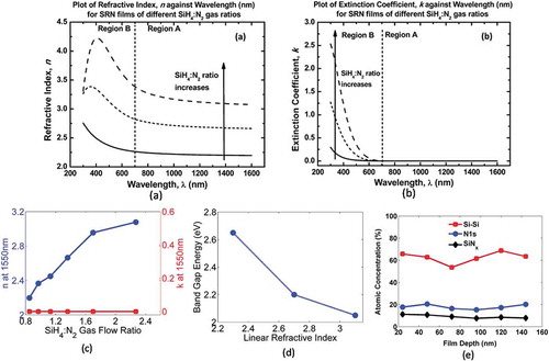
Inductively coupled CVD-grown SRN films at a temperature of 250°C were studied by varying the SiH4:N2 precursor gas fluence ratio, where SiH4 and N2 serve as the source of Si and N in the SRN film, respectively. Consequently, a higher SiH4:N2 ratio leads to greater silicon content in the film: As may be seen from ), as the ratio is increased from 0.85 to 2.27, the films’ refractive index change increases, varying between 2.2 and 3.1 at a wavelength of 1550 nm ()) [Citation10,Citation11]. The extinction coefficient of the films is also observed to increase more rapidly at shorter wavelengths as the SiH4:N2 ratio increases ()). Nevertheless, k is characterized to be zero at 1550 nm for all the SiH4:N2 ratios used in the study ()). The films with the highest refractive index (n = 3.1) have been characterized by X-ray photoelectron spectroscopy to possess a Si:N ratio of 7:3 and a bandgap of 2.1 eV [Citation19]. Engineering of the bandgap is shown to be possible by tailoring the film composition. ) shows the decrease in the film’s bandgap energy as the deposited films’ refractive index increases, bringing about a concomitant increase in the onset wavelength for two-photon absorption (TPA). A smaller refractive index brings with it a weakened ability to engineer dispersion, and a reduction in the nonlinear refractive index according to Miller’s rule. Therefore, it appears that careful engineering might yield a SRN film which possesses just the right bandgap to eliminate TPA, and a large nonlinear refractive index and linear refractive index to provide flexibility for dispersion engineering needed in many nonlinear optics applications. XPS measurements also corroborate the Si:N content in these films. ) shows the measured atomic concentration of Si-Si, Si-N and N1s bonds within a USRN film. An elevated Si concentration is observed, and the ratio of Si:N is extracted to be approximately 7:3. This composition corresponds to what we have come to term ultra-silicon-rich nitride (USRN), by virtue of its high silicon content.
Figure 1. (a) Refractive index as a function of wavelength for silicon-rich nitride films grown using low-temperature (250 °C) inductively coupled chemical vapor deposition. The measured refractive index of films increases as the SiH4:N2 ratio increases. (b) The measured extinction coefficient as a function of wavelength. At shorter wavelengths, the extinction coefficient becomes larger for higher silicon content. (c) The measured refractive index at 1550 nm as a function of SiH4:N2 precursor gas ratio. Varying the SiH4:N2 ratio from the smallest to largest value results in a variation of the refractive index from 2.2 to 3.1. (d) The measured band gap energy vs. film refractive index. An inverse relation is observed. (e) Atomic concentration of the Si-N, Si- Si and N1s bonds within a USRN film as a function of film depth, measured using X-ray photoelectron spectroscopy. From Ref. 10 and 19
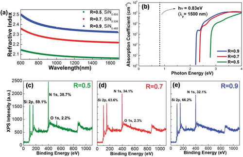
Lin et al. have previously demonstrated low-temperature, plasma-enhanced chemical vapor deposition (PECVD) growth of SRN utilizing SiH4 and NH3 precursor gases [Citation12,Citation13]. In this work, the source of nitrogen in the SRN film is derived from NH3 rather than N2. shows the use of SiH4:NH3 gas ratios which vary from 0.5 to 0.9 to achieve different n vs. λ profiles in the grown SRN films. In their film growth, PECVD parameters include a radio frequency power of 100 W, substrate temperature of 350°C and a pressure of 134 Pa. The obtained refractive index at 1550 nm ranges from 2.05 to 2.26 and 2.36, with a higher refractive index coincident with a higher SiH4:NH3 precursor gas ratio. The measured Si content is further quantified using X-ray photo-electron spectroscopy (XPS) measurements to vary from 59.1% to 66.2%.
Figure 2. (a) Refractive index vs. wavelength profile of PECVD grown SRN films, using SiH4 and NH3 precursor gases. R denotes the ratio between SiH4 and NH3. It is observed that larger R results in higher Si content and larger refractive indices. (b) A shift in the absorption coefficient vs. photon energy curve to higher photon energies is observed as R is decreased. (c) – (e) X-ray photo-electron spectroscopy measurements of the Si and N content in the films with various R values. From Ref. 12
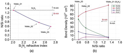
While CVD deposition techniques offer an excellent design capability to vary the refractive index of the grown films, it has been shown that the Si content should not be arbitrarily increased to be as high as possible: too high and TPA can emerge at the 1550 nm wavelength region. Indeed, it was previously shown in PECVD grown films that the transition between TPA-free and TPA-present SRN can occur when the silicon content is too high [Citation22]. In this work, PECVD grown SRN films are deposited using SiH4 and N2 at a temperature of 350°C. As the N2 gas flow rate was kept constant, the SiH4 gas flow rate was increased from 1.8 sccm to 3.6 sccm and 7.2 sccm ()). The smallest SiH4 flow rate of 1.8 sccm resulted in films with a refractive index of 2.01, close to that of stoichiometric silicon nitride. The film refractive index is observed to increase as SiH4 flow rate is increased, reaching a value of 2.71 when SiH4 flow rate is 7.2 sccm. The films are characterized using Fourier transform infrared spectroscopic (FTIR) measurements to quantify the bond concentrations within the film. Through measurements of the bond concentration for Si-Si and Si-H bonds, it is observed that a higher SiH4 flow rate leads to films with higher Si content and refractive index ()). Of note, the deposited films are reported by Lacava et al. to cross over from a TPA-free to TPA-present regime as the SiH4 flow rate is doubled from 3.6 sccm to 7.2 sccm. Consequently, careful exploratory growth of SRN films for optimal nonlinear optics is important to determine the growth regimes in which nonlinear absorption emerges at the wavelength of interest, especially when tuning the films towards a higher refractive index. In another work utilizing LPCVD growth techniques, the refractive index of the SRN films was shown to be tunable from 1.98 to 2.18 [Citation14]. In these films, the N and Si source was derived from NH3 and SiH2Cl2 (dichlorosilane (DCS) gas). It is interesting to note that, in this work, it was reported that the higher refractive index films corresponding with n = 2.18 (DCS: NH3 = 12) had a smaller measured film stress than the lower refractive index film with n = 1.98 (DCS: NH3 = 0.3). In the latter, films started to exhibit signs of stress-related bending and cracking, similar to that which has been reported in the growth of thick Si3N4 films, necessary to access the anomalous dispersion regime in Si3N4 waveguides [Citation31].
Figure 3. (a) N/Si ratio as a function of the refractive index of PECVD grown SRN films. Wafer 1 is similar to Si3N4, marking the boundary between N-rich and Si-rich films. (b) Chemical bond concentration as a function of N/Si ratio showing the increase in Si-Si and Si-H bond concentration when N/Si ratio decreases. From Ref. 31
In general, the various reports of SRN film growth have shown a common theme, that is the ability to compositionally tune the real part of the refractive index, bandgap, and by extension, the two-photon edge of the materials. However, there are some noteworthy differences in each of these reports. There exist a wide range of film growth process conditions that various groups have adopted, such as temperature and precursor gases. Temperature, in particular, turns out to be a rather significant parameter, as it appears to limit (1) the range of achievable film refractive indices and (2) front end of the line (FEOL) and/or back end of the line (BEOL) CMOS compatibility. In Ref. 13 where SRN film growth used high temperatures (800°C), a smaller range of achievable refractive indices was reported. We postulate that the high deposition temperature results in a more extensive formation of Si-N bonds, and somewhat limits the extent of silicon content within the film matrix and, by extension, range of achievable refractive indices. In addition, thermal budgets for FEOL exceed 1000°C to accommodate processes such as spike or flash annealing. For BEOL CMOS-compatibility, it should be noted that far lower thermal budgets (<400°C) are allowed; beyond this temperature, melting of copper and dopant migration within P–N junctions formed at the front-end will occur.
The mitigation of TPA at telecommunications wavelengths is one of the critical advantages in which SRN has over silicon-based nonlinear optics. TPA in silicon waveguides causes light at higher powers to be attenuated. TPA in silicon is further exacerbated by the generation of free carriers, which cause free-carrier absorption and cause its own nonlinear phase shifts from free carrier dispersion. The presence or absence of TPA may be engineered by utilizing films which have a material bandgap that is larger than the two-photon energy for photons at 1550 nm (1.6 eV), importantly with a buffer to account for band tail states (Urbach tails). For example, in amorphous silicon films, it has previously been reported that even films with a material bandgap of 1.7 eV exhibit residual TPA at 1550 nm [Citation32]. In USRN, the material bandgap, Eg is compositionally engineered to be sufficiently larger than 1.7 eV (Eg = 2.1 eV). Therefore, a sufficiently large bandgap that precludes two-photon transitions at a specific wavelength of operation is key to eliminating TPA[Citation32].
Nonetheless, SRN films may be fabricated with processes which are standard in CMOS manufacturing, thus benefiting from the economies of scale and ease of integration with CMOS electronics. For this reason, as well as advantageous nonlinear optical properties to be discussed in this article, SRN is a unique and promising platform for the implementation of nonlinear optical processes, overcoming the issues associated with nonlinear losses in silicon, and availing an optical nonlinearity that increases with the silicon-richness of the films.
For the rest of this review, we focus on the recent progress in nonlinear optics applications made in USRN, which possesses one of the highest refractive indices across the spectrum of SRN compositions that have been demonstrated for nonlinear optics. This property gives USRN a strong silicon-like behavior in that it has a large Kerr nonlinearity and waveguide nonlinear parameter, while at the same time having an important optical property possessed by stoichiometric silicon nitride, which is the absence of TPA at the 1550 nm wavelength. These attributes have made USRN a very promising platform on which to implement CMOS-compatible nonlinear optics devices, importantly at low optical powers and highly compact footprints. Advancements in the design, fabrication and experimental observation of soliton behavior at low powers and high gain optical parametric amplification (OPA) are discussed. In addition, we shed light on the utility of USRN for fully harnessing slow light enhancements without minimal concomitant scaling in nonlinear losses. Finally, the future outlook of USRN-based nonlinear optics is discussed[Citation49].
2. Nonlinear ultra-silicon-rich nitride photonics devices
USRN is typically grown using SiH4 and N2 precursor gases at a low temperature of 250°C using inductively coupled chemical vapor deposition. The low deposition temperature makes it compatible with backend CMOS processing. USRN has a high proportion of silicon content relative to nitrogen (Si:N = 7:3). Its linear refractive index was previously characterized using FTIR to be 3.1 at a wavelength of 1550 nm [Citation19].
To shed light on USRN’s nonlinear optical properties, open and closed aperture z-scan measurements have previously been performed on USRN films at a wavelength range from 800 nm to 1600 nm [Citation33]. The 1.1 -μm-thick USRN films were deposited onto silicon dioxide (50 μm thick). Due to the small sample thickness, the measured z-scans will encounter only a small aggregate nonlinearity over a finite sample thickness. Consequently, the valley-peak in the signal will be small, placing a requirement on a very high signal-to-noise ratio in the measurement. This high signal-to-noise ratio is achieved by employing a fast z-scan method. The optical pulses used for the z-scan measurements within the measurement wavelength range are derived from an optical parametric amplifier pumped using a Ti:Sapphire laser, generating 150 fs pulses at a repetition rate of 1 kHz.
) shows the measured nonlinear refractive index of USRN measured using closed aperture z-scan measurements. It is observed that the nonlinear refractive index measured at 1.55 μm is 2.9 × 10⁻¹⁷ m2/W. In addition, self-phase modulation experiments in USRN waveguides have previously been performed to extract the nonlinear refractive index at 1.55 μm. The 1.8-ps pulses propagating through a USRN waveguide with a width of 600 nm and height of 300 nm undergo different extents of self-phase modulation at different peak powers. ) shows the measured and modelled self-phase modulation spectra at various peak powers. The modelling is performed using the nonlinear Schrödinger equation (NLSE). The best match between the modelled and measured SPM spectra occurs at a nonlinear parameter of 550 W−1/m and zero TPA. The strong nonlinear parameter in USRN waveguides is achieved through (1) a large linear refractive index of 3.1 that allows for high modal confinement and (2) a large Kerr nonlinearity in the USRN platform. Using the calculated effective area of the USRN waveguide (0.21 μm2) and the equation for the nonlinear parameter, , we can extract the nonlinear refractive index of USRN to be 2.8 × 10⁻¹⁷ m2/W, very close to the value obtained using z-scan measurements [Citation11]. This value is 5–6 times larger than silicon [Citation34,Citation35], and 2 orders of magnitude larger than in stoichiometric silicon nitride [Citation36,Citation37].
Figure 4. a) The nonlinear refractive index of USRN measured using closed aperture z-scan (black squares) measurements and self-phase modulation experiments in USRN waveguides (red star). (b) Multi-photon absorption coefficients of USRN in the IR range characterized using z-scan measurements. (c) Measured and (d) modelled self-phase modulation as a function of peak power of 1.8 ps pulses propagating through a USRN waveguide with a width and height of 600 nm and 300 nm respectively. From Refs. 33 and 34
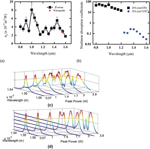
Further insight may be obtained about the nonlinear properties of USRN using open aperture z-scan measurements. It is observed from ) that TPA vanishes at a wavelength of 1.2 μm. Beyond this wavelength, three-photon absorption is the dominant contributor to nonlinear absorption. While the three-photon absorption mechanism is a significantly less deleterious effect on the efficiency of nonlinear optics than TPA, it could still come into play at very high powers or in the presence of slow-light effects. This will be further discussed in Section 6. It is further observed from ) that the TPA extends slightly beyond the theoretical two-photon edge (Eg/2). Due to the amorphous nature of USRN, band tail states exist, also known as Urbach tails, which further extend to the two-photon region [Citation38]. Nevertheless, the measurement confirms that the 1550-nm region is free of TPA.
The absence of TPA at 1550 nm implies that the efficiency of nonlinear processes does not deteriorate at higher powers. When combined with a large linear and nonlinear refractive index, USRN waveguides may be designed and engineered to possess nonlinear parameters 500× larger than in stoichiometric silicon nitride waveguides. In many Kerr-based nonlinear processes, the nonlinear effect scales nonlinearly with the nonlinear parameter. In four-wave mixing and optical parametric gain, for example, the conversion efficiency/gain scales with the square of the nonlinear parameter [Citation39]. Therefore, a large nonlinear parameter provides operational gains where high nonlinear conversion is desired in a regime where power needs to be relatively low.
In general, the treatment of nonlinear dynamics in USRN waveguides is performed using the NLSE. Compared to silicon where the presence of TPA and free-carrier absorption introduces additional loss terms to the equation, modelling of nonlinear pulse propagation dynamics takes on a simpler form [Citation39,Citation40]:
where z is the longitudinal coordinate, α is the linear loss coefficient, A and T are the slow varying pulse envelope and time, respectively. βk represents dispersion of various orders. The nonlinear parameter, , where ω0 is the frequency, n2 is the nonlinear refractive index of the material, Aeff is the effective area of the waveguide. In the presence of slow-light effects, such as in photonic crystal waveguides and nonlinear Bragg gratings, γ in EquationEq. (1)
(1)
(1) is replaced by an effective nonlinear parameter,
where ng is the group index and no is the refractive index of the material. The slow-light factor, . In slow-light devices, higher order dispersion often needs to be considered, since the magnitudes of the dispersion for all orders are often orders of magnitude larger than in waveguides. The significance of the dispersion of a specific order can be evaluated by the dispersion length
, where x is the dispersion order and T0 is the pulse half-width (at 1/e-intensity point) [Citation39]. If the total device length exceeds these dispersion lengths, then that particular dispersion order will have a sufficiently significant effect on the nonlinear dynamics and needs to be considered in the calculation.
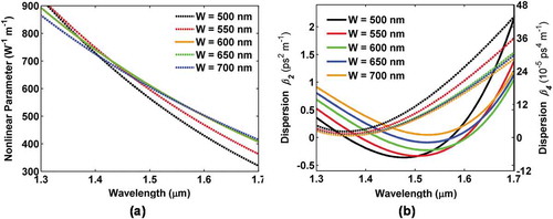
USRN photonic devices typically utilize SiO2 as a cladding. In addition to enabling high modal confinement, the large index contrast between USRN and SiO2 (nUSRN – nSiO2 = 1.54) provides an important flexibility in engineering varying magnitudes of either normal or anomalous dispersion by tailoring the waveguide geometry. ) shows the magnitudes of nonlinear parameters that can be achieved in USRN waveguides with a fixed height of 300 nm, as the width is varied from 500 nm to 700 nm. ) further plots the second- and fourth-order dispersion of USRN waveguides as a function of geometry, for a fixed waveguide height of 300 nm. For example, USRN waveguides with a height and width of 300 nm and 600 nm possess a nonlinear parameter of 550 W−1/m while simultaneously possessing anomalous dispersion.
Figure 5. (a) Calculated nonlinear parameter of USRN channel waveguides for a fixed height of 300 nm and as function of waveguide width, W. (b) The calculated second-order (β2, solid lines) and fourth-order (β4, dashed lines) dispersion of the USRN waveguides as a function of W for a fixed height of 300 nm. From Ref. 19
Fabrication of USRN photonic devices typically starts with film deposition using inductively coupled CVD at a temperature of 250°C, followed by electron beam lithography, inductively coupled plasma etching and plasma enhanced CV of the SiO2 cladding.
3. High gain optical parametric amplification in USRN waveguides
Anomalous dispersion is a necessary ingredient for a whole suite of nonlinear optics applications. These include parametric processes, observation of soliton dynamics and temporal pulse compression. Parametric wavelength conversion, for example, which requires phase matching for optimal conversion efficiency across a broad bandwidth, is a key driver for wavelength multicasting [Citation41], optical regeneration [Citation42] and OPA [Citation43]. Parametric wavelength conversion based on the Kerr nonlinearity is a four-wave mixing process whereby a pump photon at frequency, ω1 and signal photon at ω2 are annihilated to create a photon each at ω3 and ω4. In the case of degenerate four-wave mixing, two pump photons create a photon each at the signal and idler wavelength [Citation39,Citation44]. This process is one where momentum is conserved and phase matching is required. For the four-wave mixing process to take place efficiently, the phase mismatch between the pump and signal needs to be minimized. The phase mismatch Δk, in turn, depends on the effects of both cross-phase modulation and self-phase modulation. Δk = 2.γPpump – Δklinear where the linear-phase mismatch, Δklinear = – β2(Δω)2 – β4(Δω)4/12, β2,4 are the second- and fourth-order dispersion and ∆ω is the frequency difference between the pump and signal. β4 only plays a stronger role close to the zero dispersion wavelength, where the magnitude of β2 becomes small. The relationship between the frequencies of each of the four photons in the four-wave mixing process is given by ω3 + ω4 = ω1 + ω2. In the case of degenerate four-wave mixing, the relationship between the frequencies of the pump photons (ωpump), signal (ωsignal) and idler (ωidler) photons is given by 2ωpump = ωsignal + ωidler. We further note that operating in the single-mode regime further enforces mixing of only the fundamental modes of the pump and signal fields.
One recent demonstration which utilizes degenerate four-wave mixing and showcases the advantageous nonlinear optical properties of USRN waveguide devices involves the generation of giant optical parametric gain [Citation19]. In this work, the USRN photonic waveguides are dispersion engineered for anomalous dispersion at the 1550 nm wavelength region and the geometry tailored for high modal confinement. Prior to this work, CMOS-compatible OPA had taken place in several other platforms with varying degrees of success [Citation43–46]. The impact of TPA on the parametric gain process may be inferred from Si-waveguide-based OPAs when operating at 1550 nm (TPA and FCA present) and at 2200 nm (TPA and FCA free): When operating at the TPA-free wavelength of 2200 nm, optical parametric gain of 25.4 dB [Citation43] was achieved as opposed to 5 dB when operating at 1550 nm where TPA and FCA are present [Citation47]. In these experiments, the pump-signal detuning is relatively small and therefore the difference in the observed parametric gain arises from the nonlinear parameter and the presence/absence of TPA in each of the waveguides. Despite the smaller modal confinement (and hence nonlinear parameter) of the silicon waveguide at a wavelength of 2200 nm, the parametric gain was observed to be significantly larger at 2200 nm compared to 1550 nm, as a result of the absence of TPA. Furthermore, the optical parametric gain was observed in Ref. 59 to saturate at peak pump powers exceeding 2 W – a phenomenon which was not observed at the TPA-free wavelength of 2200 nm. Furthermore, in Hydex glass, despite the lower nonlinearity than silicon, a parametric gain of 15 dB has been demonstrated using waveguides with a nonlinear parameter of 0.22 W−1/m and a zero TPA at 1550 nm, revealing that the presence of nonlinear losses is far more important than the magnitude of the nonlinearity itself [Citation48]. A better parametric gain of 26.5 dB was demonstrated in amorphous silicon waveguides at 1550 nm, which possess a larger nonlinearity and smaller TPA coefficient than crystalline silicon [Citation45].
Using USRN waveguides, 600 nm in width and 300 nm in height, we degenerate four-wave mixing experiments using a pulsed pump, and CW signal is performed to investigate the efficiency of the waveguides in generating high parametric gain. The pump pulses are derived from a mode locked fiber laser at a repetition rate, Rp of 20 MHz. The 2.0-ps hyperbolic secant pulses centered at 1560 nm, at a peak power of 10 W, are used in the first set of OPA experiments. The pump and signal are combined using a wavelength division multiplexer, and both fields are aligned for transverse-electric (TE) polarization. ) shows the resulting four-wave mixing spectra, measured using an optical spectrum analyzer. Sidebands around the CW signal form which are characteristic of cross-phase modulation occurring between the CW signal and the pulsed pump. The spectral shape of the idler is also observed to assume a form similar to that of the 500 fs pump. Similarly, when a 2-ps pump is used ()), the idler assumes a form that is similar to the spectral shape of the 2-ps pump. It should be noted that owing to the pulsed nature of the pump, the mixing between pump and signal only occurs at a time interval of 1/Rp. This phenomenon is taken into account when calculating the optical parametric gain. The on/off signal parametric gain is given by Ppeak(s)/Pout(s), where Pout(s) is the CW signal power at the waveguide output when the pump is off. In general, the peak power of the amplified signal or idler may be calculated using the following equation:
Figure 6. (a) Transmission spectrum of four-wave mixing occurring between a 2.0 ps pump with a peak power of 10 W and a CW signal, as the CW power is varied. The black line shows the pump spectrum (offset by −15 dB) with the CW signal [Citation80] off. The power of the generated idler scales linearly with the signal power. Black solid curve represents the pump spectrum offset by −15 dB, without the signal turned on. Cyan, yellow, green, blue and red lines represent the measured spectra with a signal power of −21.1 dBm, −16.1dBm, −13.7 dBm and −11.0 dBm respectively. The inset shows the location of the spectral peak in the first idler as a function of signal wavelength. (b) The measured signal gain as a function of signal power. The signal gain stays constant as signal power is increased while the amplified signal power scales linearly with signal power. (c) Four-wave mixing spectrum as a function of signal wavelength for 500 fs pump pulses at a peak power of 14 W. Cascaded four-wave-mixing is observed, with the second and third idlers located close to 1410 nm and 1300 nm. The measured pump spectrum, offset by −25 dB with the CW signal off is shown as the grey dashed curve. (d) Measured parametric gain in the signal (blue squares), first (red circles), second (dark blue stars) and third idlers (green diamonds). From Ref. 19
![Figure 6. (a) Transmission spectrum of four-wave mixing occurring between a 2.0 ps pump with a peak power of 10 W and a CW signal, as the CW power is varied. The black line shows the pump spectrum (offset by −15 dB) with the CW signal [Citation80] off. The power of the generated idler scales linearly with the signal power. Black solid curve represents the pump spectrum offset by −15 dB, without the signal turned on. Cyan, yellow, green, blue and red lines represent the measured spectra with a signal power of −21.1 dBm, −16.1dBm, −13.7 dBm and −11.0 dBm respectively. The inset shows the location of the spectral peak in the first idler as a function of signal wavelength. (b) The measured signal gain as a function of signal power. The signal gain stays constant as signal power is increased while the amplified signal power scales linearly with signal power. (c) Four-wave mixing spectrum as a function of signal wavelength for 500 fs pump pulses at a peak power of 14 W. Cascaded four-wave-mixing is observed, with the second and third idlers located close to 1410 nm and 1300 nm. The measured pump spectrum, offset by −25 dB with the CW signal off is shown as the grey dashed curve. (d) Measured parametric gain in the signal (blue squares), first (red circles), second (dark blue stars) and third idlers (green diamonds). From Ref. 19](/cms/asset/f75e3fc2-cf52-4641-83ab-72918ebbdb98/tapx_a_1905544_f0006_oc.jpg)
where Rp is the pulse repetition rate of 20 MHz and Tpulse is the pulse width [Citation19,Citation43,Citation45]. The subscripts s and i(n) refer to the signal or nth idler. Pave(s,i)(λ) represents the average output power spectrum of the signal as a function of wavelength measured by the OSA. In deriving Ppeak(s), the power residing in the continuous-wave signal line is subtracted from the spectrum of Pave(s)(λ). The optical parametric gain is extracted to be 30 dB when 2-ps pulses at a peak pump power of 10 W are used. The spectral feature observed in ) between 1400 nm and 1450 nm represents evidence of cascaded four-wave mixing.
Next, the peak power of the pump pulses is increased by utilizing 500-fs pulses for the pump, with a peak power of 14 W. ()) shows the four-wave mixing spectrum measured where evidence of cascaded four-wave mixing is observed. Generation of the second and third idlers centered close to 1410 nm and 1300 nm, respectively, is clearly observed, together with the measured pump spectrum, offset by −25 dB with the CW signal off. The observation of cascaded four-wave mixing is further evidence of the strength of the parametric process occurring. It is further observed that the gain sidebands residing around the signal have considerable spectral content from the mixing with the spectrally broader pump. The optical parametric gain achieved for a peak power of 14 W is 42.5 dB. The idler conversion efficiency may further be extracted using the ratio, Ppeak(i(n))/Pout(s) where the peak power in the nth idler may be found using EquationEq. (3)(3)
(3) . It is observed from ) that the idler conversion exceeds 0 dB for all three idlers, possessing a value of 36.2 dB, 21.2 dB and 7.7 dB for the first, second and third idlers, respectively. As a result of cascaded four-wave mixing, the output spectrum spans from 1300 nm to beyond 1700 nm, with each idler providing as a source of photons for four-wave mixing. The results show that high conversion and high efficiency parametric amplification are possible in USRN waveguides.
4. Optical parametric gain in photonic crystal waveguides
Photonic waveguides in USRN provide high-light confinement conducive to large nonlinear parameters. An alternate light-guiding mechanism may be implemented by enforcing a periodicity in two-dimensions, together with the introduction of a line defect in order to create photonic crystal waveguides [Citation49]. The interaction between the gap guided and index guided modes results in a slow-light effect at the band edge of the photonic crystal waveguide [Citation50]. The reduced group velocity in such waveguides leads to a better interaction of the propagation of light waves with both the guiding material and its immediate environment. Slow-light photonic waveguides may, therefore, lead to enhanced nonlinear effects. Low-power parametric wavelength conversion [Citation51], enhanced optical modulation [Citation52] and soliton-effect compression [Citation53,Citation54] are some examples of phenomena that have been facilitated by photonic crystal waveguides. Consequently, two-dimensional photonic crystals have made a significant impact, enabling low-power operation and ultra-small chip sizes for various nonlinear optical phenomena to be observed.
Slow-light scaling of the nonlinear parameter follows the form given by EquationEq. (2(2)
(2) ), introducing an avenue to increase nonlinear effects through augmented group indices. On the flipside, slow-light scaling also causes nonlinear absorption effects to be more pronounced. In silicon photonic crystal waveguides, the severity of two-photon and free-carrier absorption increases with the square of ng [Citation51] according to the same slow light factor, which similarly augments the nonlinear parameter.
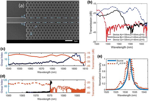
USRN photonic crystal waveguides have been demonstrated to possess large group indices between 22 and 110, depending on whether flatband engineering is incorporated [Citation21]. In these photonic crystal waveguides, row shifts of the row immediately adjacent to the line defect on either side are performed to create the flatband slow light effect. The row shift parameter is denoted by s1, as shown in ()). The radius, r and lattice constant, a are also important design parameters of the photonic crystal waveguides. The effects of these parameter changes on the photonic crystal transmission spectrum are shown in ). shows the measured group index vs. wavelength for flatband engineered and non-flatband engineered USRN photonic crystal waveguides, respectively. In these devices, USRN is 300 nm thick, surrounded by an SiO2 over- and under-cladding. The photonic crystal waveguide’s device parameters are r = 125 nm, s1 = 30 nm and a = 420 nm. From ), it is observed that flatband engineering creates a broader wavelength range from 1600 nm to 1605 nm over which a group index of ~20 is observed, while simultaneously possessing high transmissivity. Conversely, in the absence of flatband engineering, the group index is observed to increase to a very large value of 110, though this comes at a tradeoff of significantly smaller bandwidth. The group index of the flatband engineered photonic crystal waveguide is further characterized using self-phase modulation experiments. The nonlinear phase of a short pulse scales with the slow-light factor (see EquationEq. (2(2)
(2) )) according to the equation,
, where L is the photonic crystal waveguide length and Pin is the peak power of the input pulse. Therefore, the extent of self-phase modulation occurring at a fixed pulse peak power can be used to extract ng. The 1.9-ps sech2 pulses from a mode-locked fiber laser (20 MHz repetition rate) with a peak power of 2.5 W are launched into a photonic crystal waveguide with r = 135 nm and s1 = 30 nm. When the pulses with a peak power of 2.5 W are tuned to the slow-light region, a nonlinear phase shift of 1.5π is observed ()), allowing us to extract a nonlinear parameter of 1.97 × 10⁴ W−1/m, equivalent to a group index of 22 and slow-down factor of 484. This enhancement in the nonlinear parameter may further reduce the powers required for the observation of nonlinear optical phenomena.
Figure 7. (a) Scanning electron micrograph of a photonic crystal waveguide in USRN. The parameters, r (radius), s1 (shift in the row immediately beside the line defect) and a, lattice constant, set to be 420 nm. (b) Transmission spectrum of a photonic crystal waveguide for various values of r and s1. s2 refers to the shift in the row second from the line defect. Transmission (black/blue) and group index (orange) measurements of (c) non-flatband engineered and (d) flatband engineered USRN photonic crystal waveguide. (e) Self-phase modulation of a pulse with Pin = 2.5 W observed when propagating in the slow-light region of the USRN photonic crystal waveguide. From Ref. 21
The reduced group velocity at the photonic crystal band edge has been shown to augment the interaction of an optical field with the nonlinearity of the medium in which it propagates in. The efficiency of parametric wavelength conversion may likewise benefit from slow-light enhancements. Using 97 μm-long USRN photonic crystal waveguides, four-wave mixing experiments are performed, in particular to harness the enhanced nonlinearity brought about in the slow light region [Citation55]. The photonic crystal waveguides have a thickness of 300 nm, r = 105 nm, s1 = 40 nm and a = 430 nm.
Within the slow light region, the propagation loss is characterized to be (22 ± 2) dB/cm. We note that the pump-signal detuning is small (less than 10 nm), and therefore group velocity dispersion’s impact on phase matching is minimal. The photonic crystal waveguide used has a group index spectrum as shown in ()). It is observed that a flat-band region with a span of around 10 nm exists, where the group index is close to 20 within the flat-band slow-light region. We performed four-wave mixing experiments using a 9-ps pulsed pump at a repetition rate of 20 MHz centered at 1551 nm. A continuous wave signal is combined with the pump pulses using a 3-dB coupler before coupling into the photonic crystal waveguide. Power dependent measurements are first performed using a CW signal wavelength of 1554.6 nm. ) shows the four-wave mixing spectrum as the peak power of the pump is varied between 0.26 W and 2.6 W. In the four-wave mixing spectra, it is observed that sidebands develop around the CW signal. These sidebands are characteristic of parametric mixing with the pulsed pump, causing a spectral feature to arise that is similar in shape to that of the pump. The peak power of the signal and idler at the output of the photonic crystal waveguide may be calculated using EquationEq. (3)(3)
(3) . Finally, the on/off optical parametric gain of the signal is given by Psignal,peak/Psignal,out.
Figure 8. (a) Group index vs. wavelength of the USRN photonic crystal waveguide used for four-wave mixing experiments. (b) Four-wave mixing spectrum for a 9 ps pump centered at 1554.6 nm nm and signal centered at 1555 nm, as a function of signal power. (c) Experimentally measured (circles) and theoretically calculated (red solid line) conversion efficiency as a function of coupled input peak power. (d) Experimentally measured (circles) and theoretically calculated (blue solid line) signal gain as a function of coupled input peak power. A gain of 3 dB is observed at a coupled input peak power of 2.6 W. From Ref. 55
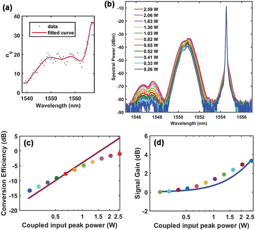
) shows the trend of idler conversion efficiency and signal gain as a function of the pump power; It is observed that both metrics increase with pump peak power. It is further observed from ()) that at 2.6 W, parametric gain of the signal reaches a value of 3 dB, corresponding with a per unit length optical parametric gain of 333 dB/cm. The idler conversion efficiency is also shown in ()). Theoretical calculations of the expected idler conversion efficiency and signal parametric gain is also shown in ()). The theoretical gain coefficient, , where γeff is the effective nonlinear parameter, Pin is the coupled peak power of the pump, β2 is the group velocity dispersion of the photonic crystal waveguide, Ω is the detuning between the pump and the signal [Citation51,Citation55,Citation56]. The four-wave mixing conversion efficiency may then be calculated using the expression, CE = (γeffPinsinh(gL)/g)2.e−αL. Parametric gain of the signal, Gsignal = 1 + CE. The loss parameter, α = 510 m−1 (22 dB/cm) and γeff = 5.5
103 W−1/m. In calculating the conversion efficiency, we assume an undepleted pump and absence of TPA. Good agreement between the experimentally measured and theoretically predicted parametric gain as a function of pump power is observed in ()).
In ()), a gradual plateau in the idler conversion efficiency is observed at higher peak powers, deviating from the theoretically calculated curve. The origin of this effect is likely nonlinear absorption. While the nonlinear parameter scales with S2, the slow-down factor also contributes towards intensifying the effects of nonlinear loss mechanisms if present. While TPA is absent at 1550 nm, three-photon absorption could still possibly be observed at sufficiently high powers or a sufficiently large slow-down factor. The lower than expected idler conversion efficiency observed in experiments could therefore originate from the non-trivial scaling of three-photon absorption in photonic crystal waveguides [Citation57]. Nevertheless, the absence of TPA in the USRN photonic crystal waveguides makes the four-wave mixing and OPA process significantly more efficient than in devices where TPA is present. This is evidenced in the large gain of 333 dB/cm demonstrated in sub-100 μm USRN photonic crystal waveguides. Compared to OPA in USRN waveguides, photonic crystal waveguides provide a higher per unit gain in more compact device footprints.
5. Soliton-effect compression in USRN photonic waveguides
The demonstration of high gain OPA is possible because of the ability to efficiently generate large nonlinear effects at lower powers with minimal optical losses. The presence of anomalous dispersion was also essential for phase matching to occur in the degenerate four-wave mixing process. The nonlinear efficiency of the USRN platform may be further demonstrated for the observation of temporal soliton dynamics, which benefits from the preservation of the pulse energy at high powers as high order solitons form and evolve. Across the spectrum of CMOS-compatible waveguides, one of the first observations of soliton effects was in Hydex waveguides. Adiabatic soliton compression in Hydex glass waveguides were demonstrated for 1.6× compression of 0.65 ps pulses to 0.40 ps [Citation58]. Stronger temporal compression of 2.3× has been demonstrated in silicon photonic crystal waveguides, as a result of the strong band edge dispersion, slow light scaling of the nonlinear parameter, though this is likewise accompanied by a similar scaling in the two-photon and free-carrier absorption [Citation53]. High order solitons form in media with nonlinearity and anomalous dispersion, and experience an initial narrowing at the beginning of each soliton period. Strong temporal compression is therefore possible with waveguides which are appropriately designed, together with the right pulse powers. Both the pulse peak power and dispersion determine the soliton number, N. In general, photonic waveguides with high modal confinement possess shorter nonlinear lengths compared to dispersive lengths, conditions that make it easy to generate high order solitons. Furthermore, a larger soliton order implies a potentially greater compression factor, provided the propagation length is designed to coincide with the point at which the temporal width of the soliton is narrowest as it evolves through the waveguide. For N ≥ 10, the optimal length, zopt = 1.6z0/N, where z0 = πLd/2 is the soliton period and Ld is the dispersion length [Citation39,Citation59].
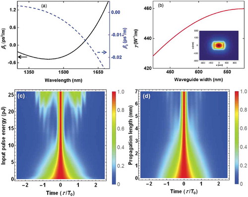
Temporal compression of optical pulses provides a route for generating ultrashort pulses or to augment the peak powers of pulses. High order soliton compression in USRN waveguides have been recently used to demonstrate 8.7× compression of optical pulses using pulse energies as low as 16.3 pJ [Citation60]. Pulse propagation dynamics through 7 mm long, SiO2 cladded USRN waveguides with a width and height 450 nm and 330 nm respectively were first studied using the nonlinear Schrodinger equation (EquationEq. 1)(1)
(1) and found to allow strong compression while preserving the pulse energy. The dispersion of the waveguides is designed to be anomalous ()). The nonlinear parameter of the waveguide is further calculated to be 440 W−1/m ()). In the simulations, it is observed from ()) that as the input pulse energy is increased to 16 pJ – 20 pJ, the temporal pulse width of 2.0 ps pulses decreases monotonically to 230 fs. Beyond a pulse energy of 23 pJ, the compressed pulses start to acquire increasing levels of pulse pedestals while not incurring any further decrease in the compressed pulse width. When observing the output pulse profile at a fixed pulse energy of 16.3 pJ as a function of USRN propagation length, an initial pulse narrowing is observed as theoretically expected ()). It is further observed from ()) that an optimum propagation length of ~3.5 mm exists, corresponding with the strongest pulse compression. As the propagation length increases beyond this value, pulse pedestals start to develop.
Figure 9. (a) Calculated second and third order dispersion for an SiO2 cladded USRN waveguide with a width and heigth of 450 nm and 330 nm respectively. (b) Calculated nonlinear parameter of USRN waveguide with a heigth of 330 nm as a function of waveguide width at a wavelength of 1550 nm. (c) Numerical calculations of the pulse propagation dynamics through a 7 mm USRN waveguide as a function of input pulse energy. (d) Numerically calculated output pulse profile at a fixed pulse energy of 16.3 pJ as a function of propagation length. From Ref. 60
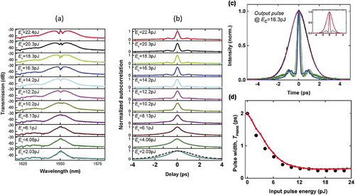
The soliton dynamics initiated in USRN waveguides are experimentally studied using 2.0 ps pulses at a repetition rate of 20 MHz, centered at a wavelength of 1550 nm. The propagation losses of the waveguides used was 3 dB/cm. The pulses are adjusted for TE-polarization prior to coupling into the USRN waveguide using tapered lensed fibers. Spectral and temporal properties of the optical pulses are characterized using an optical spectrum analyzer and autocorrelator respectively. The pulses at the USRN waveguide output are studied as a function of input pulse energy. It is expected that the pulse width should experience a narrowing initially as input pulse energy is increased. ()) show the spectral and temporal evolution as a function of the input pulse energy. It is observed that the spectral content increases as the pulse energy increases. Temporally, the output pulses experience a narrowing as the pulse energy is increased. ()) shows the measured (green circles) and numerically calculated (blue solid line) autocorrelation traces of the output pulse at an input pulse energy of 16.3 pJ. The measured input pulse profile is shown as the solid black line. The experimentally measured output pulses are in excellent agreement with the numerically calculated results. As a control experiment, the output pulses measured when bypassing the USRN waveguide are measured when the input pulse energy is 16.3 pJ. In this case as shown in the solid fuchsia line in ()), there is no compression observed when the pulses do not propagate in the USRN waveguide. ()) further plots the calculated compression factors of the pulses as a function of the input pulse energy. It is observed that as the input pulse energy increases to 16.3 pJ, the compressed pulse width decreases quickly. Beyond this value of input pulse energy, the compression factor increases marginally. The measured autocorrelation trace width reaches its minimum value of 360 fs at an input pulse energy of 22.4 pJ. This corresponds to a pulse width of 230 fs (applying a 1.54 deconvolution factor to the autocorrelation trace for sech2 pulse), corresponding to a compression factor of 8.7 × . This represents the strongest on-chip soliton-effect compression to date. Certainly, further refinements in the operating regime and USRN waveguide length could advance the extent of soliton-effect compression achieved. For example, given the initial narrowing that is experienced under conditions supporting high order solitons, higher pulse energies combined with shorter USRN waveguides could allow maximum pulse narrowing to coincide with the output of the waveguide, and is therefore an important area for further study.
Figure 10. (a) Spectral and (b) temporal (autocorrelation) traces as a function of input pulse energy. The autocorrelation trace of the 2.0 ps pulses is shown as the black dashed line. (c) Comparison of experimental (green circles) and calculated (blue solid line) output pulse autocorrelation at an input pulse energy of 16.3 pJ. The measured input pulse profile is shown as the solid black line. The output pulses when bypassing the USRN waveguide (with input pulse energy of 16.3 pJ) is plotted as the solid fuchsia line. No compression is observed in this case. The inset shows the measured input and output pulses (gray hollow circle) fitted with the sech2 function (red dashed line). (d) Experimentally measured (black circles) and theoretically calculated (solid red line) pulse width (FWHM) plotted as a function of input pulse energy. From Ref. Citation61
6. Nonlinear Bragg gratings in USRN
Soliton effects in USRN waveguides show great promise for creating strong temporal compression. Owing to the abilty to engineer large amounts of anomalous dispersion at the band edge, photonic crystal waveguides are another possible avenue for implementing high-order soliton compression [Citation53,Citation54] which could likewise be implemented on the USRN platform. While photonic crystal waveguides rely on a periodicity in two-dimensions to create a photonic bandgap, Bragg gratings introduce a photonic bandgap by enforcing a periodicity in one dimension. In 1985, Winful theoretically prediceted that an optical field propagating close to the stopband of a fiber Bragg grating experiences a region of high group velocity dispersion, a phenomenon that arises due to the interaction between forward and backward propagating fields from the artificial bandgap [Citation47]. Experimental corroboration of the large grating-induced dispersion was demonstrated in 1996 by Eggleton et. al [Citation62]. In this work, temporal compression of optical pulses was demonstrated in fiber Bragg gratings through an interplay bewteen the fiber nonlinearity and the grating-induced dispersion. The blue side of the stopband in particular, exhibits large anomalous dispersion. The optical fiber, being fabricated out of silica, did not possess any nonlinear absorption effects at the wavelength of the experiment (1550 nm), and therefore allowed high powers needed to approach the high-order soliton regime needed to create the compression effect. Close to the blue side of the photonic bandgap, the group index increases rapidly, giving rise to an increased magnitude of anomalous group velocity dispersion while maintaining a high transmission. This augmented group index may also be leveraged similarly to the slow light enhancements in photonic crystal waveguides.
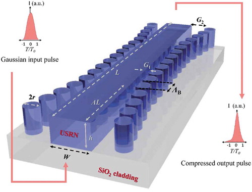
With the advent of CMOS-compatible USRN which possesses a Kerr nonlinearity that is two orders of magnitude larger than in silica glass, or nonlinear waveguide parameter that is five orders of magnitude larger than in single mode fiber, nonlinear on-chip Bragg grating devices could similarly be applied towards low power, grating enhanced observations of soliton dynamics. On-chip gratings, implemented using pillars placed periodically alongside a waveguide may be used for this purpose. These gratings, termed cladding-modulated Bragg gratings (CMBGs), have been successfully demonstrated to provide high dispersion in reflection when the period of the CMBGs is chirped [Citation63–65]. However, it is the disperison in transmission that we harness for nonlinear optical effects.
shows the schematic of a USRN CMBG designed for operation at 1550 nm [Citation66]. A central waveguide with a width of 600 nm and height of 300 nm is flanked by cylinders on either side with a period Λ. The gap between the pillars and central waveguide varies from 150 nm to 50 nm. This essentially serves the function of apodization, which ensures that the change in the effective index experienced by an optical field incident on the grating occurs gradually. Consequently, the grating sidelobes are effectively suppressed without impacting the Bragg wavelength (λB = 2neff Λ). Implementation of the apodization follows the following function:
Figure 11. Schematic of a USRN CMBG. The strong grating-induced dispersion at the band edge combined with the strong waveguide nonlinearity allows high-order solitons to form. From Ref. 66
where
where AL = 600 µm. The total CMBG length, L is 6 mm.
In principle, when an optical pulse is tuned close to the blue side of the grating stopband, it experiences a large magnitude of anomalous dispersion, which can be several orders of magnitude larger than the native dispersion of the waveguide. To further understand the optical properties of the CMBG, the transmission and dispersion of the fabricated device are experimentally measured. A scanning electron micrograph of the fabricated CMBG before SiO2 deposition is shown in ()).
Figure 12. (a) Scanning electron micrograph of a USRN CMBG before SiO2 deposition. (b) Transmission spectrum, (c) ng (blue), β2 (red), (d) β3 (green) and β4 (cyan) as a function of wavelength of the USRN CMBG. The crosses denote the wavelength of the picosecond pulses launched into the CMBG. From Ref. 66
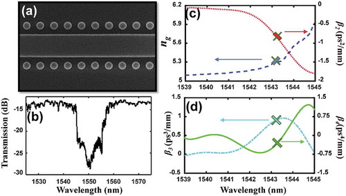
The linear transmission properties of our grating are characterized using an amplified spontaneous emission source adjusted for TE polarization and an optical spectrum analyzer. ()) shows the transmission spectrum of the CMBG. The center of the CMBG stopband is close to 1.55 μm. The dispersion properties of the grating are experimentally measured by extracting the ng vs. λ properties using an interferometry-based component analyzer. The dispersion parameters are derived from the polynomial fitting of the group index curve shown in ()) using the expression, , where n is the order of dispersion and β is the propagation constant. The experimentally extracted group velocity dispersion (GVD, β2), third-order dispersion (TOD, β3) and fourth-order dispersion (FOD, β4) curves are shown in ()) respectively. At a wavelength of 1543.1 nm, the grating dispersion parameters are extracted to be, β2 = −0.81 ps2/mm, β3 = 0.83 ps3/mm, β4 = −0.33 ps4/mm (denoted by crosses in ()) and 12d). We note that the group velocity dispersion in USRN waveguides are three orders of magnitude smaller [Citation19]. Consequently, the grating structure induces a band edge dispersion that is three orders of magnitude larger than in USRN waveguides, importantly while still being within a region of high transmission. For a pulse full-width at half-maximum of 4.93 ps, the dispersion lengths [Citation39] corresponding to the values of β2,3,4 are calculated to be LD2 = 10.8 mm, LD3 = 31.3 mm and LD4 = 23.3 cm at λ = 1543.1 nm. LD2 and LD3 are sufficiently small that GVD and TOD will have a significant effect on the nonlinear pulse propagation dynamics whereas FOD effects will conversely be negligible.
To harness the USRN CMBGs towards soliton dynamics, we study the pulse propagation dynamics of TFWHM = 4.93 ps Gaussian pulses (where for Gaussian pulses) in the wavelength region where both dispersion and transmission are high. ()) shows the spectrum (centered at 1543.1 nm) and temporal profile of the pulses. At this wavelength, ng = 5.3 ()), giving rise to a slow-light enhancement in the nonlinear parameter by a factor of 3. For a fixed pulse peak power, the soliton order, N may be derived using the expression,
where Pin refers to the peak power. In the absence of perturbative effects (i.e. TOD, FC and TPA), an N = 1 soliton propagating through the waveguide preserves its shape over the propagation length; this corresponds to a fundamental soliton. Higher-order solitons exhibit more complex temporal dynamics. They periodically compress, split into multiple pulses, and recover their original shape over a single soliton period, defined as z0 = π/2 × LD2 [Citation39]. When TOD effects are sufficiently large, the delicate balance of GVD and SPM may be perturbed, causing the soliton to deviate from the expected symmetric and periodic evolution. In the absence of TOD or any other perturbative effects, the fundamental solitons comprising a higher-order soliton are bound and exist as a breather, propagating at identical speeds. The presence of TOD breaks that degeneracy and causes the separation of higher-order soliton into its constituents. These separated solitons then travel further apart from each other in the guiding media rather than evolving back into their initial pulse shape at z = z0. As a result of the large third order dispersion in the USRN CMBG, we expect that at a sufficiently large power, a high order soliton could be observed to break down into its constituent fundamental solitons, giving rise to fission.
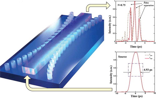
Figure 13. Temporal and spectral characterization of the pulses at the CMBG output. Measured spectrum and temporal profile of (a) the source pulse, soliton evolution for (b) N = 2.22 (P0 = 0.36 W), (c) N = 4.65 (P0 = 1.62 W) and (d) N = 8.75 (P0 = 5.73 W) for Lg = 4.8 mm. From Ref. 66
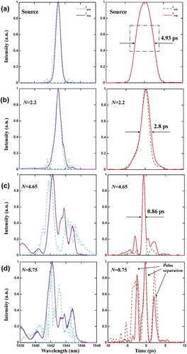
Frequency resolved electrical gating (FREG) is used to characterize the temporal profile of the output pulses as the peak power of the input pulses is increased. FREG allows both pulse intensity and phase to be extracted, thus allowing any distinct pulse peaks to be clearly observed. shows the time resolved traces of the output pulses at various powers. Higher peak powers correspond to higher soliton orders. At the lowest peak power corresponding to a soliton order of 2.2, the pulses are observed to compress to 2.8 ps ()). As the power is increased further to N = 4.65, the pulse compression becomes stronger, and pulses are compressed to 0.86 ps ()). The level of compression corresponds with a 5.7× compression factor, stronger than that previously demonstrated in silicon photonic crystal waveguides. At the highest powers used in the experiment (N = 8.75), three distinct peaks emerge in the output pulse ()). The separation of these pulses from the primary pulse is characteristic of soliton fission occurring. The observations of Bragg soliton compression and soliton fission are greatly facilitated by both device and material properties: (1) The high-quality grating ensures that the sharp increase in group index as the wavelength is tuned close to the stopband does not have phase or magnitude discontinuities. (2) The absence of TPA allows the Bragg soliton dynamics to proceed unhindered, while the large nonlinearity of USRN allows rich Bragg soliton dynamics to manifest over short length scales. (3) Fission is triggered by the large magnitude of third order dispersion. The successful demonstration of Bragg-soliton compression and fission warrants further study into how they may be harnessed for chip-scale nonlinear applications.
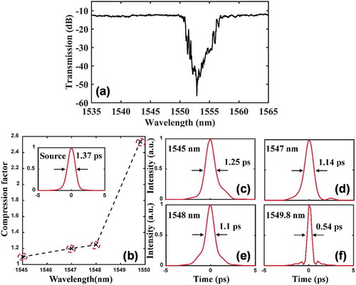
To further shed light on the dynamics of pulse propagation dynamics, wavelength dependent measurements are performed, where the input pulse wavelength is tuned from 1545 nm to 1549.8 nm. This allows the input pulses to access increasing magnitudes of β2 as its wavelength approaches the grating stopband. One of the signatures of Bragg solitons is their dependence on wavelength. This effect arises because of dispersive properties vary rapidly with wavelength, as may also be observed in ()). ()) shows the transmission spectrum of a 3 mm long grating used for this experiment. It is observed from (–f)) that the temporal compression of a 1.37 ps pulse increases as the pulse wavelength is tuned closer to the grating stopband. At the smallest stopband-pulse detuning (1549.8 nm), the pulse experiences the strongest compression, reaching a FWHM of 0.54 ps.
Figure 14. (a) Transmission spectrum of grating used for wavelength dependent compression measurements, where the input pulse wavelength is tuned from 1545 nm to 1549.8 nm. (b) Experimentally measured compression factor as a function of wavelength. Inset shows the temporal profile of the source pulses. (c-f) Temporal measurement of optical pulses using frequency resolved electrical gating at input pulse wavelengths of (c) 1545 nm, (d) 1547 nm, (e) 1548 nm and (f) 1549.8 nm. From Ref. 66
7. Future outlook and conclusions
The recent advancements made in USRN-based nonlinear optics span from high gain OPA, including a giant gain per unit length in photonic crystal waveguide OPAs (333 dB/cm) and soliton dynamics in both waveguides and nonlinear Bragg gratings. Given the sensitivity of the USRN CMBGs to wavelength, the implementation of thermo-optic control of these grating devices could provide a pathway towards active, on-demand tuning of pulse properties. In addition to the order of magnitude larger Kerr nonlinearity in USRN vs. Si3N4, USRN has recently also been found to possess a large thermo-optic coefficient, an order of magnitude larger than that in Si3N4 [Citation67]. Other formulations of SRN have also been reported to possess a large thermo-optic coefficient [Citation68]. This feature could therefore be used for low power thermo-optic based tuning of nonlinear USRN Bragg grating phenomena.
Opportunities for further advancing the material platform exist. Although annealing at temperatures as high as 1200 °C is a well known approach for reducing losses in Si3N4 films [Citation1,Citation2,Citation4], approaches which reduce losses through other means, if available, are more desirable if backend CMOS compatibility is a consideration. For the reduction of Si-H bond related losses, recipes which utilize alternative gases other than silane could be explored. Dichlorosilane gas (DCS, SiH2Cl2) is one possible alternative to silane which could be explored for further optimization of the USRN films [Citation69], specifically to reduce losses originating from Si-H and N-H bonds. Other approaches adopted in stoichiometric silicon nitride fabrication could also present possible pathways towards further device optimization. The photonic damascene process relies on depositing Si3N4 on a highly smooth, pre-patterned oxide preform and subsequent chemical mechanical polishing to remove the excess Si3N4 material [Citation31]. This approach has yielded Si3N4 resonators with quality factors on the order of 106 [Citation70].
Similar to the growth of SRN-based nonlinear photonics, chalcogenide-based nonlinear photonics though not CMOS-compatible, has seen significant sucess due to low TPA at the 1550 nm wavelength regime [Citation71]. On-chip optical parametric gain [Citation72], supercontinuum generation [Citation73–76], correlated photon pair generation [Citation77], wavelength conversion of high speed data [Citation78] and notably Brillouin scattering [Citation79] in recent years have been demonstrated in chalcogenide platforms. In addition to being TPA-free, USRN further possesses larger waveguide nonlinear paramters than chalcogenide waveguides, offering the potential for lower power nonlinear optics. Of note, the aforementioned possible routes towards optimizations in the fabrication processes could be instrumental to further reducing losses. Consequently the developmental prospects of USRN-based nonlinear applications appear promising. For example, Brillouin scattering, Raman effects or possible interfacial stain engineering towards introducing a second-order nonlinearity in USRN devices could be pertinent nonlinear effects worth investigating. Applications which leverage the already well-established Kerr nonlinearity in USRN also present multiple near-term advancement opportunities, ranging from phase sensitive parametric amplifiers, lower power frequency combs and Bragg soliton phenomena. Building upon the studies of how solitons form in both USRN waveguides and photonic crystal waveguides, these studies will be advanced towards investigating ways in which soliton-effect compression and fission can be applied towards enhancing the generation of coherent supercontinuum. It is further envisioned that future work will investigate more sophisticated manipulations of dispersion of various orders and applications which efficiently handle high speed data, or which shape or manipulate optical waveforms with precision. Systems requiring nonlinear components, including optical metrology tools [Citation48,Citation70,Citation80,Citation81], frequency combs [Citation1–18] and tunable ultrafast pulse sources could also be worthwhile topics of investigation which may similarly benefit from the high Kerr nonlinearity and two-photon free operation at telecommunications wavelengths.
Lastly, it is worthwhile to note that even though USRN possesses advantageous nonlinear properties at the telecommunications wavelength, like silicon, it does not possess a direct bandgap necessary for lasing. Consequently, a USRN-based nonlinear device which incoporates the light source would involve heterogeneous integration, similar to that which has been successfully demonstrated in Si3N4-based frequency combs pumped using III–V lasers [Citation82,Citation83]. The field of III–V lasers has advanced so tremendously that their lasing properties and form factors are highly conducive to integration with photonic integrated circuits [Citation84,Citation85]. Consequently, these advantageous complementary technologies could instrumental towards the deployment of USRN devices which integrate not only light sources but also the CMOS-based ASICs necessary to drive the electronics within the on-chip system. Indeed, the prospects for further development in USRN-based nonlinear optics appear promising, with many exciting developments which further leverage complementary photonics technologies to come.
Acknowledgments
This work was supported by the National Research Foundation Competitive Research Grant (NRF-CRP18-2017-03) and MOE ACRF Tier 2 Grant (MOE2016-T2-2-155). This work is a collaboration project between SUTD and IME (A*STAR).
Disclosure statement
No potential conflict of interest was reported by the authors.
Additional information
Funding
References
- Moss DJ, Morandotti R, Gaeta AL, et al. New CMOS-compatible platforms based on silicon nitride and Hydex for nonlinear optics. Nat Photonics. 2013;7:597–34.
- Pfeiffer MHP, Kordts A, Brasch V, et al. Photonic Damascene process for integrated high-Q microresonator based nonlinear photonics. Optica. 2016;3:20.
- Pasquazi A, Peccianti M, Razzari L, et al. Micro-combs: a novel generation of optical sources. Phys Rep. 2018;729:1–81.
- Gaeta AL, Lipson M, Kippenberg TJ. Photonic chip-based frequency combs. Nat Photonics. 2019;13:158.
- Corcoran B, Tan M, Xu X, et al. Ultra-dense optical data transmission over standard fiber with a single chip source. Nat Commun. 2020;11:2568.
- Hu H, Da Ros F, Pu M, et al. Single-source chip-based frequency comb enabling extreme parallel data transmission. Nat Photonics. 2018;12:469–473.
- Marin-Palomo P, Kemal JN, Karpov M, et al. Microresonator-based solitons for massively parallel coherent optical communications. Nature. 2017;546:274–279.
- Kues M, Reimer C, Roztocki P, et al. On-chip generation of high-dimensional entangled quantum states and their coherent control. Nature. 2017;546:622–626.
- Kues M, Reimer C, Lukens JM, et al. Quantum optical microcombs. Nat Photonics. 2019;13:170–179.
- Ng DKT, Wang Q, Wang T, et al. Exploring high refractive index silicon-rich nitride films by low temperature inductively coupled plasma chemical vapor deposition and applications for integrated waveguides. ACS Appl Mater Interfaces. 2015;7:21884–21889.
- Wang T, Ng DKT, Ng SK, et al. Supercontinuum generation in bandgap engineered, back-end CMOS compatible silicon rich nitride waveguides. Laser Photon. Rev. 2015;9:498–506.
- Wu CL, Lin YH, Su SP, et al. Enhancing optical nonlinearity in a nonstoichiometric SiN waveguide for cross-wavelength all-optical data processing. ACS Photonics. 2015;2:1141–1154.
- Lin GR, Su SP, Wu CL, et al. Si-rich SiNx based Kerr switch enables optical data conversion up to 12 Gbit/s. Sci Rep. 2015;5:9611.
- Krückel CJ, Fülöp A, Klintberg T, et al. Linear and nonlinear characterization of low-stress high-confinement silicon-rich nitride waveguides. Opt Express. 2015;23:25827–25837.
- Mitrovic M, Guan X, Ji H, et al. Four wave mixing in silicon-rich nitride waveguides in Frontiers in Optics, OSA Technical Digest Series (Optical Society of America), paper FM1D.6, 2015.
- Choi JW, Chen GFR, Ng DKT, et al. Wideband nonlinear spectral broadening in ultra-short ultra-silicon rich nitride waveguides. Sci Rep. 2016;6:27120.
- Puckett MW, Sharma R, Lin HH, et al. Observation of second-harmonic generation in silicon nitride waveguides through bulk nonlinearities. Opt Express. 2016;24:16923–16933.
- Liu X, Pu M, Zhou B, et al. Octave-spanning supercontinuum generation in a silicon-rich nitride waveguide. Opt Lett. 2016;41:2719–2722.
- Ooi KJA, Ng DKT, Wang T, et al. Pushing the limits of CMOS optical parametric amplifiers with USRN:Si7N3 above the two-photon absorption edge. Nat Commun. 2017;8:13878.
- Xing P, Chen GFR, Zhao X, et al. Silicon rich nitride ring resonators for rare-earth doped C-band amplifiers pumped at the O-band. Sci Rep. 2017;7:9101.
- Sahin E, Ooi KJA, Chen GFR, et al. Enhanced optical nonlinearities in CMOS-compatible ultra-silicon-rich nitride photonic crystal waveguides. Appl Phys Lett. 2017;110:161113.
- Lacava C, Stankovic S, Khokhar AZ, et al. Si-rich silicon nitride for nonlinear signal processing applications. Sci Rep. 2017;7:22.
- Ye Z, Fülöp A, Helgason ÓB, et al. Low-loss high-Q silicon-rich silicon nitride microresonators for Kerr nonlinear optics. Opt Lett. 2019;44:3326–3329.
- Debnath K, Bucio TD, Al-Attili A, et al. Photonic crystal waveguides on silicon rich nitride platform. Opt Express. 2017;25:3214–3221.
- Lacava C, Dominguez Bucio T, Khokhar AZ, et al. Intermodal frequency generation in silicon-rich silicon nitride waveguides. Photon Res. 2019;7:615–621.
- Miller RC. Optical second harmonic generation in piezoelectric crystals. Appl Phys Lett. 1964;5:17–19.
- Lafforgue C, Guerber S, Ramirez JM, et al. Broadband supercontinuum generation in nitrogen-rich silicon nitride waveguides using a 300 mm industrial platform. Photon Res. 2020;8:352–358.
- Ay F, Aydinli A. Comparative investigation of hydrogen bonding in silicon based PECVD grown dielectrics for optical waveguides. Opt Mater. 2004;26:33–46.
- Philipp HT, Andersen KN, Svendsen W, et al. Amorphous silicon rich silicon nitride optical waveguides for high density integrated optics. Electron Lett. 2004;40:419–421.
- Mao SC, Tao SH, Xu YL, et al. Low propagation loss SiN optical waveguide prepared by optimal low-hydrogen module. Opt Express. 2008;16:20809–20816.
- Pfeiffer MHP, Herkommer C, Liu J, et al. Photonic damascene process for low-loss, high-confinement silicon nitride waveguides. IEEE J Sel Top Quantum Electron. 2018;24:1–11.
- Shoji Y, Ogasawara T, Kamei T, et al. Ultrafast nonlinear effects in hydrogenated amorphous silicon wire waveguide. Opt Express. 2010;18:5668–5673.
- Sohn B-U, Choi JW, Ng DKT, et al. Optical nonlinearities in ultra-silicon-rich nitride characterized using z-scan measurements. Sci Rep. 2019;9:10364.
- Wang T, Venkatram N, Gosciniak J, et al. Multi-photon absorption and third-order nonlinearity in silicon at mid-infrared wavelengths. Opt Express. 2013;21:32192–32198.
- Dinu M, Quochi F, Garcia H. Third-order nonlinearities in silicon at telecom wavelengths. Appl Phys Lett. 2003;82:2954–2956.
- Ikeda K, Saperstein RE, Alic N, et al. Thermal and Kerr nonlinear properties of plasma-deposited silicon nitride/silicon dioxide waveguides. Opt Express. 2008;16:12987–12994.
- Tan DTH, Ikeda K, Sun PC, et al. Group velocity dispersion and self phase modulation in silicon nitride waveguides. Appl Phys Lett. 2010;96:061101.
- Urbach F. The long-wavelength edge of photographic sensitivity and of the electronic absorption of solids. Phys Rev. 1953;92:1324.
- Agrawal GP. Nonlinear fiber optics. Academic Press, New York; 1995.
- Monat C, Corcoran B, Ebnali-Heidari M, et al. Slow light enhancement of nonlinear effects in silicon engineered photonic crystal waveguides. Opt Express. 2009;17:2944–2953.
- Biberman A, Lee BG, Turner-Foster AC, et al. Wavelength multicasting in silicon photonic nanowires. Opt Express. 2010;18:18047–18055.
- Salem R, Foster MA, Turner AC, et al. All-optical regeneration on a silicon chip. Opt Express. 2007;15:7802–7809.
- Liu X, Osgood RM, Vlasov YA, et al. Mid-infrared optical parametric amplifier using silicon nanophotonic waveguides. Nat Photonics. 2010;4:557–560.
- Foster MA, Turner AC, Salem R, et al. Broad-band continuous-wave parametric wavelength conversion in silicon nanowaveguides. Opt Express. 2007;15:12949–12958.
- Kuyken B, Clemmen S, Selvaraja SK, et al. On-chip parametric amplification with 26.5 dB gain at telecommunication wavelengths using CMOS-compatible hydrogenated amorphous silicon waveguides. Opt Lett. 2011;36:552–554.
- Wang KY, Foster AC. GHz-rate optical parametric amplifier in hydrogenated amorphous silicon. J Opt. 2015;17:094012.
- Foster MA, Turner AC, Sharping JE, et al. Broad-band optical parametric gain on a silicon photonic chip. Nature. 2006;441:960–963.
- Pasquazi A, Park Y, Azaña J, et al. Efficient wavelength conversion and net parametric gain via four wave mixing in a high index doped silica waveguide. Opt Express. 2010;18:7634–7641.
- Joannopoulos JD, Meade RD, Winn JN. Photonic crystals. Princeton Univ. Press, New York; 1995.
- Povinelli ML, Johnson SG, Joannopoulos JD. Slow-light, band-edge waveguides for tunable time delays. Opt Express. 2005;13:7145–7159.
- Monat C, Ebnali-Heidari M, Grillet C, et al. Four-wave mixing in slow light engineered silicon photonic crystal waveguides. Opt Express. 2010;18:22915–22927.
- Hinakura Y, Arai H, Baba T. 64 Gbps Si photonic crystal slow light modulator by electro-optic phase matching. Opt Express. 2019;27:14321–14327.
- Blanco-Redondo A, Husko C, Eades D, et al. Observation of soliton compression in silicon photonic crystals. Nat Commun. 2014;5:3160.
- Colman P, Husko C, Combrié S, et al. Temporal solitons and pulse compression in photonic crystal waveguides. Nat Photonics. 2010;4:862–868.
- Sahin E, Ng DKT, Tan DTH. Optical parametric gain in CMOS-compatible sub-100 um photonic crystal waveguides. APL Photonics. 2020;5:066108.
- Cestier I, Willinger A, Colman P, et al. Efficient parametric interactions in a low loss GaInP photonic crystal waveguide. Opt Lett. 2011;36:3936.
- Husko C, Combrié S, Tran QV, et al. Non-trivial scaling of self-phase modulation and three-photon absorption in III–V photonic crystal waveguides. Opt Express. 2009;17:22442–22451.
- Peccianti M, Ferrera M, Razzari L, et al. Subpicosecond optical pulse compression via an integrated nonlinear chirper. Opt Express. 2010;18:7625–7633.
- Mollenauer LF, Stolen RH, Gorden JP, et al. Extreme picosecond pulse narrowing by means of soliton effect in single-mode optical fibers. Opt Lett. 1983;8:289.
- Choi JW, Sohn B-U, Chen GFR, et al. Soliton-effect optical pulse compression in CMOS-compatible ultra-silicon-rich nitride waveguides. APL Photonics. 2019;4:110804.
- Winful HG. Pulse compression in optical fiber filters. Appl Phys Lett. 1985;46:527.
- Eggleton BJ, Slusher RE, de Sterke CM, et al. Bragg grating solitons. Phys Rev Lett. 1996;76:1627.
- Tan DTH, Ikeda K, Fainman Y. Cladding-modulated Bragg gratings in silicon waveguides. Opt Lett. 2009;34:1357.
- Sahin E, Ooi KJA, Png CE, et al. Large, scalable dispersion engineering using cladding-modulated Bragg gratings on a silicon chip. Appl Phys Lett. 2017;110:161113.
- Sahin E, Ooi KJA, Png CE, et al. On-chip large dispersion using cladding-modulated Bragg gratings. Frontier Optics 2017, Washington, D. C. United States, 18-21 September. 2017; OSA Technical Digest, FM3A.4. Part F66-F. Optical Society of America; 2020.
- Sahin E, Blanco-Redondo A, Xing P, et al. Bragg soliton compression and fission on CMOS-compatible ultra-silicon-rich nitride. Laser Photon Rev. 2019;13:1900114.
- Cao YM, Sahin E, Choi JW, et al. Thermo-optic tuning of spectral broadening in a nonlinear ultra-silicon-rich nitride grating. 14th Pacific Rim Conference on Lasers and Electro-Optics (CLEO PR 2020), Sydney, Australia, 03-05 August 2020; OSA Technical Digest, paper C3C_2. Optical Society of America; 2020.
- Nejadriahi H, Friedman A, Sharma R, et al. Thermo-optic properties of silicon-rich silicon nitride for on-chip applications. Opt Express. 2020;28:24951–24960.
- Ng DKT, Xing P, Chen GFR, et al. Improved CMOS-compatible ultra-silicon-rich nitride for non-linear optics. SPIE Photonics West; Accepted
- Pfeiffer MHP, Kordts A, Brasch V, et al. Photonic Damascene process for integrated high-Q microresonator based nonlinear photonics. Optica. 2016;3:20–25.
- Eggleton BJ, Luther-Davies B, Richardson K. Chalcogenide photonics. Nat Photonics. 2011;5:141–148.
- Lamont MRE, Luther-Davies B, Choi DY, et al. Net-gain from a parametric amplifier on a chalcogenide optical chip. Opt Express. 2008;16:20374–20381.
- Hudson DD, Dekker SA, Mgi EC, et al. Octave spanning supercontinuum in an As2S3 taper using ultralow pump pulse energy. Opt Lett. 2011;36:1122–1124.
- Choi JW, Sohn BY, Chen GFR, et al. Nonlinear characterization of GeSbS chalcogenide glass waveguides. Sci Rep. 2016;6:27120.
- Al-kadry A, El Amraoui M, Messaddeq Y, et al. Two octaves mid-infrared supercontinuum generation in As2Se3 microwires. Opt Express. 2014;22:31131–31137.
- Hu J, Menyuk CR, Shaw LB, et al. Maximizing the bandwidth of supercontinuum generation in as2se3 chalcogenide fibers. Opt Express. 2010;18:6722–6739.
- Xiong C, Helt LG, Judge AC, et al. Quantum-correlated photon pair generation in chalcogenide As2S3 waveguides. Opt Express. 2010;18:16206–16216.
- Galili M, Xu J, Mulvad HCH, et al. Breakthrough switching speed with an all-optical chalcogenide glass chip: 640 Gbit/s demultiplexing. Opt Express. 2009;17:2182.
- Eggleton BJ, Poulton CG, Pant R. Inducing and harnessing stimulated Brillouin scattering in photonic integrated circuits. Adv Opt Photon. 2013;5:536–587.
- Monat C, Grillet C, Collins M, et al. Integrated optical auto-correlator based on third-harmonic generation in a silicon photonic crystal waveguide. Nat Commun. 2014;5:3246.
- Kondo K, Baba T. On-chip autocorrelator using counter-propagating slow light in a photonic crystal with two-photon absorption photodiodes. Optica. 2017;4:1109–1112.
- Stern B, Ji X, Okawachi Y, et al. Battery-operated integrated frequency comb generator. Nature. 2018;562:401–405.
- Shen B, Chang L, Liu J, et al. Integrated turnkey soliton microcombs. Nature. 2020;582:365–369.
- Zhou Z, Yin B, Michel J. On-chip light sources for silicon photonics. Light Sci Appl. 2015;4:e358.
- Norman JC, Jung D, Wan Y, et al. Perspective: the future of quantum dot photonic integrated circuits. APL Photon. 2018;3:030901.