
 ?Mathematical formulae have been encoded as MathML and are displayed in this HTML version using MathJax in order to improve their display. Uncheck the box to turn MathJax off. This feature requires Javascript. Click on a formula to zoom.
ABSTRACT
In the domain of gas sensing, metal oxide nanostructures have been demonstrated to have very attractive properties due to their large surface-over-volume ratio, combined with the possibility to use multiple materials and multi-functional properties. Here, we review the basic physical principles underlying the transducer function of metal oxide nanostructures, from single nanostructures to nanostructure networks. These principles have been adapted to describe the response of more complex nanostructures, such as heterostructures, combining two different metal oxide materials, or a metal with a metal oxide, in order to further enhance the sensitivity and selectivity of such devices. We finally present the activation of nanostructures by light exposure as a promising alternative to the standard method based on high temperature activation, which is earning increasing consensus in the perspective of low-power Internet of Things applications.
Graphical abstract
I. Introduction
Supported by 5 G and higher-frequency communication protocols to come, the Internet of Things (IoT) era is becoming real and increasingly pervasive in our day life. If, on one side, data flow boosting and delocalized intelligence are the main themes, on the other side, data collection from the physical world by the so-called edge devices will have an unprecedentedly fundamental role, where sensors will play the main part. In this scenario, gas sensors are particularly attractive as dense and distributed networks of ultra-miniaturized sensors can provide spatial resolution to airborne chemical compounds monitoring, enabling the generation of air quality maps and the study of their correlation to the features of the monitored environment, either indoor or outdoor.
Conductometric metal oxide (MOx) gas sensors, where the sensing response relies on the variation of the electrical resistance of the MOx sensing layer, have proven to be structurally simple, relatively stable, sensitive down to ppm range with fast dynamics in response and recovery [Citation1] and producible in very small sizes, thus appearing as the ideal candidates to be integrated in IoT edge devices. However, as they operate at temperatures of several hundreds of °C in order to promote chemical reactions at the MOx surface, the electrical power required by integrated Joule-effect heater can hamper their compatibility with perspective stand-alone IoT sensing nodes. Aiming at the decrease in operational power and at improving sensing protocols by better temperature management, micro-hotplates were introduced. Originating from microelectronics technologies and belonging to the vast class of MEMS (Micro-Electro-Mechanical Systems), micro-hotplates are sub-millimetric-sized/micrometric-thick platforms hosting the gas sensitive layer, the interdigitated electrodes for the readout of the resistance of the sensing layer, and the integrated heater [Citation2–4].
Within the category of ‘semiconductor’ gas sensors, micro-hotplate-supported MOx sensors represent one of the most promising product lines of the gas sensors market, where the combination of different miniaturized sensing elements characterizes the most advanced products (e.g. Bosch BME680 and Sensirion SGR, to name a few). Low-cost, small dimension, low power consumption (besides self-diagnostics, data processing and communication capabilities) are, in fact, identified as the driving features of sensing devices that will support the proliferation of IoT applications and related commercial profitability [Citation5].
Although micro-hotplates ensure the decrease in sensor operational power by orders of magnitude in respect to traditional MOx gas sensors, the temperature of the sensing layer is basically unchanged with related drawbacks, e.g. mid-term degradation of sensing materials, electrodes, heater, or even risk of ignition of flammable atmospheres (which can hamper their use in ATEX -Atmosphères Explosives- contexts) [Citation6].
Since few decades, the research on gas sensors is exploring the opportunities offered by nanoscale homostructures and heterostructures, in order to lower the operational temperature while preserving sensitivity and fast dynamics, as well as to improve selective performances. In fact, in addition to the geometric increase in the specific surface typically shown by nanostructured materials and favouring the interactions with the surrounding atmosphere, charge transport properties in nanostructures can substantially deviate from bulk ones in force of confinement effects and of the dominant role of surfaces/interfaces on transport mechanisms. This, in turn, emphasizes phenomena occurring at nanostructure surface, as indeed the interactions with gas-phase molecules. Although thermal energy remains the main approach to promote surface reactions, others have been progressively investigated as catalytic properties of nanostructures and light activation. The possible coexistence and interplay of such a remarkable number of physical-chemical aspects in determining the charge transport properties of nanostructures makes the scientific literature on nanostructures-based gas sensors very rich, though characterized by similar story-telling with basically empiric approach: nanostructures synthesis methods, morphological-structural-electrical characterizations, and sensing performances.
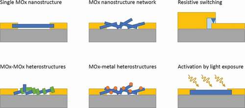
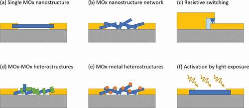
Several high-quality reviews have been published on the subject of MOx gas sensing, such as [Citation7–10] on MOx gas sensors, [Citation11–13] on MOx nanostructures for gas sensing, [Citation14–17] on MOx nanowire (NW) gas sensors, [Citation9,Citation18] focusing on MOx composites and heterostructures, and [Citation19,Citation20] for light-activated gas sensors. Nevertheless, a review specifically collecting and describing the main physical mechanisms underpinning the gas sensing properties of nanostructures is still missing. Aiming to fill this gap, we arranged this articles in three main sections dedicated to nanoscale homostructures (for simplicity ‘nanostructures’ in the following), nanoscale heterostructures (for simplicity ‘heterostructures’ in the following), and activation by light exposure, this last one addressing the main approach alternative to high temperature to promote surface reactions. The various configurations discussed in the review are schematically represented in . Three kind of homostructures are discussed, namely, single nanostructures (), nanostructure networks (), and the specifical case of resistive switching occurring in MOx thin films (). Two types of heterostructures are introduced, MOx-MOx heterostructures () and MOx-metal heterostructures (). Lastly, the effect of light on the different kind of nanostructures is discussed (). As a short review article, we will focus on the main concepts and related examples, in order to give the reader, who is not specialized in gas sensing, the background physics elements to navigate through this subject.
Figure 1. Schematic representing various conductometric device configurations discussed in the article, where the grey areas represent the substrate, the yellow areas the electrical contacts, and the blue areas the MOx nanomaterial. Three types of homostructures are discussed, (a) single nanostructures, (b) nanostructure networks, and (c) the specific case of resistive switching in thin films. Two types of heterostructures are presented, (d) one type with inclusion of a second MOx material (green areas) on the primary MOx structure (blue areas), and (e) a second type with metal particle (Orange areas) on the primary MOx structure (blue areas). (f) Lastly, we investigate the effect of light activation (yellow arrows) on the various kinds of nanostructures presented before (the blue area being replaced by any structure presented before).
In this respect, referring to the accepted paradigm according to which the gas sensing behaviour of a given system is addressed by considering a ‘receptor’ function and a ‘transducer’ function, where the former identifies the primary interaction with gas-phase molecules and relies on chemistry concepts, while the second identifies the changes in the physical properties of the system upon which an informative electrical signal is generated; it is worth underlying that this review article mainly focuses on the ‘transducer’ function, as the concepts from physics are mostlypresent here.
II. MOx nanostructure-based gas sensing
A. Sensing models
1. Introduction
The goal of the developed models is to relate the conduction properties, and more specifically the resistance of the device, to the gas partial pressure. It involves the knowledge of both the mechanism of gas adsorption on the surface (receptor function) and the response of the semiconductor to the adsorbed gas (transducer function).
For MOx, the main receptor mechanism occurs through adsorption of oxygen on the surface, which then reacts with the targeted gas. The chemical reactions occurring on the surface thus changes the surface coverage of chemisorbed oxygen, θ. On the other hand, chemisorbed oxygen modifies the surface carrier concentration of the MOx structure, ns.
For traditional MOx sensors which are made either of polycrystalline film or by assembly of nanostructures connected through their contact points, two main models have been developed in order to understand how the resistance of the sensor is modified by the change in oxygen surface coverage θ and surface carrier concentration ns. In the grain boundary model, the sensitivity occurs at the junctions between grains or nanostructures. In the surface depletion model, the bulk conduction through the nanostructure is influenced by the gas adsorption.
The typical length over which surface depletion occurs is known as the Debye length, and is given by [Citation21]:
where εr is the relative dielectric constant of the material, kB is the Boltzmann constant, T is the absolute temperature, q is the carrier charge, and nb is the bulk carrier concentration in the MOx. Two extreme cases can be distinguished depending on the nanostructure size d. For , the bulk conduction of the nanostructure is weakly affected by the gas, and the sensing response is dominated by the grain boundaries. For
, the surface depletion due to gas adsorption significantly changes the bulk conduction through the nanostructure. These two extreme models are presented in the following sections.
2. Grain boundary model
The grain boundary model has been widely applied for the understanding of polycrystalline MOx films, where the condition is usually fulfilled. In this case, the film is made of grains connected to each other through their depleted surface, as shown in (upper panel). The current through the film is limited by potential barriers occurring at the grain boundaries due to surface band bending, as shown in (lower panel). The surface band bending potential Vs can be determined by solving the Poisson equation in a 1D geometry [Citation22]:
Figure 2. Grain boundary model showing the conduction path from grain to grain (upper panel), along with the potential barriers seen by free carriers in the conduction path (lower panel). In the upper panel, the dark-grey parts represent conductive MOx, while the light-grey parts represent the surface-depleted regions. In the lower panel, xg is the grain size, w is the surface depletion width, λD is the Debye length, Ec is the conduction band minimum, and qVs is the barrier height. Adapted from [Citation22].
![Figure 2. Grain boundary model showing the conduction path from grain to grain (upper panel), along with the potential barriers seen by free carriers in the conduction path (lower panel). In the upper panel, the dark-grey parts represent conductive MOx, while the light-grey parts represent the surface-depleted regions. In the lower panel, xg is the grain size, w is the surface depletion width, λD is the Debye length, Ec is the conduction band minimum, and qVs is the barrier height. Adapted from [Citation22].](/cms/asset/7dd614ff-15b6-459f-876b-4fe057ede124/tapx_a_2044904_f0002_oc.jpg)
where w is the surface depletion width, and the calculated surface carrier concentration ns expresses as a function of bulk carrier concentration nb:
When combined with the electroneutrality at the semiconductor surface, this leads to the relationship between surface coverage and surface carrier concentration:
α being the charge of the chemisorbed oxygen species, [St] the concentration of available surface sites for oxygen adsorption. The chemical reaction occurring on the surface will give a second equation between θ, ns and the gas partial pressure, thus allowing the determination of ns vs. the gas partial pressure.
The conductance from grain to grain can be calculated in two limiting cases, the diffusion model when the barrier width 2 w is much larger than the carrier mean free path λ (), and the thermionic emission model in the opposite case (
). The conductance in each model differs mainly by the pre-factor [Citation22]:
The sensor sensitivity S given by
where G0 and Ggas are the conductance of the device exposed, respectively, to a reference gas (e.g. air) and to the targeted gas, leading to the following sensitivity for both models:
where . The knowledge of ns vs. the gas partial pressure (or concentration), along with EquationEquation (3)
(3)
(3) , will give the sensor response as a function of the gas concentration.
3. Surface depletion model
The surface depletion model is mostly applied to explain the sensing properties of MOx nanowires (NWs), for which the conductance can be easily calculated as a function of the surface depletion. The NW is approximated by a cylindrical filament of length L and diameter d. In the limit of large diameter, , we can assume that the carrier concentration in the core of the NW is unchanged by surface depletion. In this case, the relationship between the surface coverage and the surface carrier concentration ns can be calculated using the 1D Poisson equation, and is given by EquationEquation (4)
(4)
(4) . In the opposite limit of small diameter,
, the surface depletion directly impacts the carrier concentration in the core of the nanowire. In this case, the surface carrier concentration ns is obtained by solving the Poisson equation in the cylindrical geometry [Citation23]:
where nb is the bulk carrier concentration before depletion occurs, α is the charge of the chemisorbed oxygen species, and [St] is the concentration of available surface sites for oxygen adsorption. Similar to the grain boundary model, the chemical reaction occurring on the surface will give a second equation between θ, ns and the gas partial pressure, thus allowing the determination of ns vs. the gas partial pressure.
The conductance of the nanowire can be calculated in both limits of weak depletion for , and for strong depletion for
. In the weak depletion limit, as described in , a depletion layer of width w with upwards band bending is formed at the surface of the NW due to the negative charging of surface states by adsorbed oxygen species ( right). Within this model, the conductance of the depletion layer is much smaller than the conductance of the core of the nanowire, and the total conductance can be simply approximated by the conductance of a cylinder with a diameter reduced by twice the depletion layer thickness w (dark blue regions in ):
Figure 3. Surface depletion model for the NW geometry for empty surface states (left) and charged surface states (right). Ec, Ev, Ef and Ed are, respectively, the conduction band minimum energy, valence band maximum energy, Fermi level, and donor level in the MOx material. EA is the level of the surface acceptor states, and w is the depletion width. Reproduced and adapted from [Citation25].
![Figure 3. Surface depletion model for the NW geometry for empty surface states (left) and charged surface states (right). Ec, Ev, Ef and Ed are, respectively, the conduction band minimum energy, valence band maximum energy, Fermi level, and donor level in the MOx material. EA is the level of the surface acceptor states, and w is the depletion width. Reproduced and adapted from [Citation25].](/cms/asset/8bddd486-8bda-43eb-a880-fb3fd0007d46/tapx_a_2044904_f0003_oc.jpg)
where , µ0 being the carrier mobility, which is assumed to be not dependent on adsorbed gas on the surface. The depletion layer thickness is calculated [Citation24]:
assuming that the carrier concentration in the bulk is equal to the dopant concentration. The sensor sensitivity can then be expressed by:
where w0 is the depletion width without the targeted gas, and wgas is the depletion width in the presence of the gas. The knowledge of ns vs. the gas partial pressure (or concentration), along with EquationEquations (11)(11)
(11) and (Equation3
(3)
(3) ), gives the sensor response as a function of the gas concentration.
In the strong depletion limit, the carrier concentration in the core of the NW is directly controlled by the pinning of the Fermi level at the surface. In the flat band limit, this gives for the conductivity:
The sensitivity is then given by:
The knowledge of ns vs. the gas partial pressure (or concentration) gives the sensor response as a function of the gas concentration.
B. Single nanostructure
In the understanding of the role of surface depletion on the sensing properties of MOx nanostructures, important progresses have been performed on devices made on single nanostructure, which avoids the effect of averaging observed on multiple nanostructures and the potential role of junctions formed between connected nanostructures. Moreover, the use of single crystal nanostructures avoids the effect of grain boundaries in polycrystalline nanostructures. Several experiments have demonstrated the use of single nanostructures for gas sensing, most of them being dedicated to the use of MOx nanowires (NWs) [Citation26–28], which possess a good compromise between a large surface and volume ratio, and still a geometry that can be easily contacted, as compared to e.g. nanocrystals. Recent reviews give a large overview of the published works [Citation12,Citation16,Citation17]. Here, we specifically concentrate more on experiments demonstrating the sensing model.
By directly comparing the response of SnO2 thin film and SnO2 single NW to CO, CH4, H2, CO2, SO2 and H2S, Brunet et al. have shown that the NW response is larger, when rescaled to the specific adsorption surface available [Citation29]. This shows the role of the larger surface over volume ratio of NWs, for which the change of surface depletion due to the gas adsorption has a larger impact on the conductance than for thin films.
The dependence of the sensitivity of single SnO2 NW to the NW diameter has been investigated for O2 and NO2 [Citation28,Citation30]. shows the gas response to NO2 vs. N2, i.e. the resistance ratio , as a function of NO2 concentration for various NW diameters. The gas response increases when the diameter decreases, as expected from EquationEquation (13)
(13)
(13) . Moreover, the detection limit, defined by the NO2 concentration at which the signal reaches three times the standard deviation if the signal, decreases when decreasing the NW diameter, as shown in the inset of , further demonstrating the higher sensitivity when the diameter decreases. The dependence of the sensitivity as a function of NW diameter shown in can be fitted with EquationEquation (13)
(13)
(13) , which allows the authors to extract a depletion width of 10 nm for O2 [Citation30] and 13.4 ± 0.6 nm for NO2 [Citation28].
Figure 4. (a) Sensitivity of SnO2 single NW to NO2 as a function of the gas concentration and for different NW diameters. Inset: Limit of detection, defined as three times the standard deviation of the signal, as a function of NW diameter. (b) Sensitivity as a function of the NW diameter, for different gas concentrations. Reproduced from [Citation28].
![Figure 4. (a) Sensitivity of SnO2 single NW to NO2 as a function of the gas concentration and for different NW diameters. Inset: Limit of detection, defined as three times the standard deviation of the signal, as a function of NW diameter. (b) Sensitivity as a function of the NW diameter, for different gas concentrations. Reproduced from [Citation28].](/cms/asset/89b2ae30-d11c-4d27-ba84-9296c07a8634/tapx_a_2044904_f0004_oc.jpg)
The NW geometry might not be the most optimum one for enhancing the sensitivity of devices. The influence of the morphology of ZnO nanostructures for gas sensing (acetone) has been investigated using ZnO grown by hydrothermal synthesis [Citation31–33]. The sensors are fabricated by dispersing the ZnO nanostructures on predefined Au electrodes, followed by annealing at 300°C for 2 days. The maximum sensitivity is found at different temperatures depending on the geometry of the nanostructure (from 350°C to 425°C), and the sensitivity increases with the surface to volume ratio, given by the 3D-type structures.
C. Nanostructure networks
The most attractive architecture for using MOx nanostructures is the random assembly of connected nanostructures, as it can be obtained by easy and low-cost fabrication processes, such as spray deposition [Citation34] and ink-jet printing [Citation35]. In such an architecture, both the surface depletion and the junctions (acting as grain boundaries) between the nanostructures can play a role in the sensing mechanism.
1. Depletion model in nanostructure network
When contacts between nanostructures is ohmic and the nanostructures have a radial diameter of the order of the Debye length, the depletion model can be applied on the network, which is very similar to the single nanostructure device. The total response of the device can be modelled using an array of resistors [Citation36,Citation37].
This case was argued to provide a higher stability, as contacts between nanostructures might evolve over time due to sintering, which is similar to what is obtained in polycrystalline thin films [Citation38]. By using a network of single crystal SnO2 nanobelts, Comini et al. have demonstrated a very high sensitivity to NO2 and ethanol [Citation39].
2. Role of nanostructure junctions
In most of nanostructure networks, however, junctions between nanostructures play an important role in the sensing properties, following the grain boundary model. Several authors have observed a larger response of nanostructure network-based gas sensors as compared to single nanostructure, in particular for NW networks [Citation40,Citation41] or for nanoflower-like ZnO nanostructure networks [Citation42]. In these cases, the higher sensitivity as compared to MOx thin films or to single nanostructure was attributed to the presence of junctions between nanostructures. The same interpretation has been mentioned by Park et al., who demonstrated the higher sensitivity of gas sensor made of polycrystalline ZnO NWs as compared to single crystal NWs [Citation43].
While most of the published works are restricted to comparing the response magnitude of sensors in order to show the influence of junctions between nanostructures, Khan et al. have compared the sensor response kinetics [Citation44]. ZnO NW network shows a slower recovery kinetics as compared to single ZnO NW, which is interpreted by the diffusion of the gas under test (H2) through the junctions, a phenomenon that is not present in single NWs.
3. Disentangling the role of junctions and core conduction
An interesting way to disentangle the contribution of junctions vs. core conduction in the sensor response to gas is to analyse the current-voltage (I–V) characteristics, as the conduction models for junctions leads to a non-linear I–V curve, while the core conduction is expected to be linear. The non-linear conduction model through multiple junctions between nanostructures can be derived from models developed in granular thin films [Citation45,Citation46], where the voltage drop U across the device is expressed as a function of the voltage drop across individual junction Uj:
Here, Rs is an effective series resistance coming from the bulk conduction through the nanostructures and Nj is the average number of junctions along the conduction path. The current through the junction is assumed to be dominated by thermionic emission in usual temperature ranges, which gives, for double junctions:
where the two terms correspond to the two sides of the junction. Here, ni is the ideality factor of the junction [Citation21] and the values of I1 and I2 are given by the barrier height qVs and the Richardson constant A:
Caicedo et al. have investigated the relative contribution of the junctions vs. the bulk conduction in ZnO nanowire networks by changing the device geometry and analysing the non-linear I–V characteristics [Citation47]. They further analyse the dependence of the core conduction, given by the resistance Rs, and the barrier height as a function of oxygen concentration. shows the various parameters extracted from the fit of the curves with EquationEquations (17)
(17)
(17) and (Equation18
(18)
(18) ) as a function of oxygen concentration. The sensitivity to oxygen occurs through both the dependence of the series resistance Rs () and the barrier height φB ()), which directly impacts the pre-factors I1 and I2 (), while the junction number and ideality factor remain unchanged (. The dependence of Rs can be well fitted with the surface depletion model (see fit in ), while the dependence of φB can be well fitted by the grain boundary model (see fit in ), showing how both mechanisms can be disentangled. Lastly, an interesting result is that the dominating mechanism, i.e. depletion vs. junction sensing, can be modulated by the applied bias voltage, due to the different dependences on bias voltage of both mechanisms [Citation47].
Figure 5. Parameters of the fit of non-linear I–V characteristics of ZnO NW network using the thermionic emission model, respectively, (a) the series resistance Rs, (b) the effective junction number nNj, (c) the pre-factors I1 and I2, and (d) the barrier height ΦB, as a function of the oxygen concentration. Lines are fitted with the surface depletion model in (a) and the grain boundary model in (d). Reproduced from [Citation47].
![Figure 5. Parameters of the fit of non-linear I–V characteristics of ZnO NW network using the thermionic emission model, respectively, (a) the series resistance Rs, (b) the effective junction number nNj, (c) the pre-factors I1 and I2, and (d) the barrier height ΦB, as a function of the oxygen concentration. Lines are fitted with the surface depletion model in (a) and the grain boundary model in (d). Reproduced from [Citation47].](/cms/asset/505c9c58-ba88-4e92-8e96-a7f659e313f6/tapx_a_2044904_f0005_oc.jpg)
4. Advantages of nanostructure networks
One advantage of nanostructure networks already mentioned is the higher sensitivity due to the influence of junctions between nanostructures. Another important advantage is the higher device yield due to lower dispersion of the electrical characteristics, demonstrated by Zhang et al. for ZnO NW networks [Citation40], which is explained by an averaging effect when multiple nanostructures are connected in parallel and/or in series. Lastly, Sysoev et al. have shown the advantage of NW networks vs. nanoparticle films for long-term stability [Citation38]. They explain this difference by the sintering of nanoparticles under working conditions for nanoparticle films, which is not seen in percolating NW networks.
D. Resistive switching
More recently, a new type of sensing mechanism was revealed in MOx nanostructures based on resistive switching. Resistive switching devices, also known as memristor, are a strongly growing topic in the field of memory and neural network applications [Citation48,Citation49]. They rely on the bistable change in the resistance as a function of the applied electric field due to a microscopic change in conduction path, leading to a reproducible switching between a low-resistive state (LRS) and a high-resistive state (HRS). While the switching is usually produced by the applied electric field, an external stimulus such as light or the chemical environment changes can also induce the switching. Early experiments have demonstrated the interest of memristive devices for sensing, e.g. for light or pH sensing [Citation50,Citation51]. The switching mechanism is then expected to lead to a large response to the stimulus, and thus a large sensitivity.
In memristor devices based on MOx semiconductors [Citation52], the switching is attributed to the migration of dopants through the applied electric field, leading to the formation of conducting paths at the atomic scale, which can be suppressed by reversing the electric field. The large resistive switching in MOx has been more specifically explained by the forming and rupture of filaments of oxygen vacancies, which act as doping in MOx semiconductors [Citation53,Citation54]. shows the proposed mechanisms for the formation of conducting filaments, where the release of oxygen from the MOx bulk (first panel in ) creates a conducting filament of oxygen vacancies (second panel in ). Under upwards electric field, oxygen migrates and leads to an extension of the filament to the electrode, thus leading to the LRS (third panel in ). When the electric field is reversed, the migration of oxygen is reversed, breaking the filament and leading to the HRS (fourth panel in ). The last two steps are reversible, leading to the RESET and SET cycle.
Figure 6. Principle of resistive switching in MOx thin films, where the release of oxygen atoms (first panel) leads to the formation of conductive oxygen vacancies filament (second panel). The formation or rupture of oxygen vacancies filaments can be induced by an electric field acting on the migration of oxygen in the MOx, leading to the switching of the resistance from LRS (third panel) to HRS (fourth panel). Reproduced from [Citation53].
![Figure 6. Principle of resistive switching in MOx thin films, where the release of oxygen atoms (first panel) leads to the formation of conductive oxygen vacancies filament (second panel). The formation or rupture of oxygen vacancies filaments can be induced by an electric field acting on the migration of oxygen in the MOx, leading to the switching of the resistance from LRS (third panel) to HRS (fourth panel). Reproduced from [Citation53].](/cms/asset/522ca131-ea4e-4748-b001-6428546d031b/tapx_a_2044904_f0006_oc.jpg)
Gas sensors based on resistive switching in MOx nanostructures have then been proposed and demonstrated, where the interaction of the gas with the MOx layer leads to local change of doping and to switching. Nyenke et al. have investigated the effect of NO2 and NH3 gases on the resistive switching in a W/CuxO/Cu heterojunction at room temperature, showing a suppression of the switching behaviour after gas exposure [Citation55]. Based on the very high sensitivity of Pt/TiO2/Pt heterostructure to H2 at room temperature, at the condition that the distance between Pt electrodes is below 100 nm [Citation56], which is a geometry similar to memristors, Vidis et al. have proposed a memristor-based gas sensing device [Citation57]. The principle is described in . The typical hysteretic curve of memristor with HRS and LRS () is modified by the global change in resistance of the device with gas exposure (), leading to two hysteretic curves (). By current biasing the device, if the device is prepared in the HRS for gas concentration A at point 1, a change in the gas concentration to concentration B will change the voltage to point 2, where resistive switching occurs, leading to the LRS at point 3 (see ). The chosen device geometry and response to gas are shown in . shows a schematic cross-section of the device with top electrode (TE) and bottom electrode (BE), while shows a top SEM image of the device. Here, the functional MOx material is TiO2. The response curve to H2 is shown in , where the number 1, 2, and 3 in correspond to the same numbers in . When H2 exposure is stopped (point 1), the resistance of the MOx material starts to increase up to point 2, where the resistance switching occurs as it reaches the switching threshold, leading to the LRS at point 3. The response is, however, not reversible, as exposing the device to H2 does not lead a switching back (point 4), but rather to a slight change in the resistance (see inset of ). The device can then be reset to the HRS by applying an appropriate bias voltage.
Figure 7. (a–c) Principle of the resistive switching-based gas sensor, showing (a) the hysteretic curve without gas exposure, (b) the change in resistance of the MOx material under gas exposure and (c) the two hysteretic curves with and without gas, with the points 1, 2, and 3 depicting the states reaches in the preparation (1), under gas exposure (2), and after the switching induced by gas exposure (3). (d) Cross-section of the TiO2-based memristor device optimised for gas sensing, with platinum top electrode (Pt-TE) and bottom electrode (Pt-TE). (e) Scanning electron microscope (SEM) image of the real device, showing both electrodes. (f) Response curve of the device to H2, showing the points where the resistance starts to increase due to the change in the gas environment (point 1), then when it reaches the resistance switching threshold (point 2), leading to a jump of the resistance to the LRS (point 3). Under exposure to H2 again, the device does not recover (points 4 and 5) and only shows a weak change due to the change in the MOx resistance (inset). Reproduced from [Citation57].
![Figure 7. (a–c) Principle of the resistive switching-based gas sensor, showing (a) the hysteretic curve without gas exposure, (b) the change in resistance of the MOx material under gas exposure and (c) the two hysteretic curves with and without gas, with the points 1, 2, and 3 depicting the states reaches in the preparation (1), under gas exposure (2), and after the switching induced by gas exposure (3). (d) Cross-section of the TiO2-based memristor device optimised for gas sensing, with platinum top electrode (Pt-TE) and bottom electrode (Pt-TE). (e) Scanning electron microscope (SEM) image of the real device, showing both electrodes. (f) Response curve of the device to H2, showing the points where the resistance starts to increase due to the change in the gas environment (point 1), then when it reaches the resistance switching threshold (point 2), leading to a jump of the resistance to the LRS (point 3). Under exposure to H2 again, the device does not recover (points 4 and 5) and only shows a weak change due to the change in the MOx resistance (inset). Reproduced from [Citation57].](/cms/asset/275a1f25-bc02-4713-b03a-eb20477ca23c/tapx_a_2044904_f0007_oc.jpg)
Finally, the resistive switching mechanism has also been used to tune the selectivity and allow a fast recovery of ZnO NW gas sensors [Citation58]. In this device, the response to NO2 is maximum in the LRS, while it is negligible in the HRS. The behaviour is opposite for NH3, which shows no response in the LRS and a maximum response in the HRS. This selectivity can be explained by the different conduction mechanisms in the LRS and HRS. The conduction in the LRS is dominated by the NW conduction due to the high electron concentration, which is more sensitive to NO2, while the conduction in the HRS is dominated by Schottky barriers at the contacts, which are more sensitive to NH3. On the other hand, the faster recovery is obtained after using a RESET/SET operation, which is explained by Joule heating during the high voltage pulses used during the RESET/SET operations.
III. MOx-based heterostructures
Miller et al. define heterojunction as a physical interface between two dissimilar materials and a heterostructure as one that incorporates all three, two dissimilar materials and a heterojunction between them [Citation8]. Dissimilar materials, as specified by the name, will have different band gap and thus different Fermi levels. At a heterojunction, there is an exchange of charge carriers which leads to Fermi level adjustment between the two dissimilar materials. Heterostructures can be MOx-MOx or metal-MOx. We consider both in detail separately.
A. MOx-MOx heterostructures
The use of heterostructures is known to offer many advantages in enhancing the sensitivity and selectivity of gas sensors, reducing operating temperature, being prone to light activation, etc. These advantages are due to synergic physical effects arising by the combination of dissimilar materials. For example, in a heterostructure, the receptor and transducer functions can be separately optimised by choosing a receptor MOx having affinity for adsorption [Citation59], reaction [Citation60], or degradation of a target gas [Citation61], while the materials used for optimising the transducer function should have tuneable charge transport characteristics [Citation8]. The difference in bang gap and Fermi energy levels of dissimilar materials can enhance charge carrier separation, which in turn increases the charge carrier lifetime and allows them to participate in chemical reactions at MOx surface. This effect is predominantly utilised when heterostructures are used in combination with light activation [Citation62] as described in section IV.
1. Mechanisms
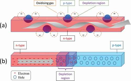
Primarily, gas sensing mechanism in heterostructure can be classified in two categories: conduction channel mechanism and potential energy barrier mechanism, as described in .
Figure 8. Schematic representation of (a) conduction channel mechanism (b) potential energy barrier mechanism of gas sensing in MOx-MOx heterostructures. Red area represents n type MOx, while blue area represents p type MOx. The depletion region is represented by purple or a mixture of red and blue. Gray arrows represent the current flow through the device. Orange coloured dashed empty circles are representative of adsorbed oxygen in (a). ‘-’ represents electrons and small circles represent holes as described in the legend.
Conduction channel
In the conduction channel mechanism, as shown in (a), the depletion or accumulation region formed at the heterojunction impinges on the conduction channel through the primary MOx with transducer function. Here, it is assumed that the movement of charge carriers is taking place in the bulk of the transducer-MOx and thus forms a conduction channel. When another MOx nanostructure is in contact with the transducer-MOx, depending on its majority carriers, a depletion or an accumulation region is formed at the interface or at the heterojunction. If the dimensions of this transducer-MOX nanostructure are comparable to twice the Debye length, any changes in the width of the depletion or accumulation region will have a direct effect on the amount of current flowing through the device. These changes occur due to oxygen adsorption and desorption along the surface of the heterostructure [Citation63,Citation64].
Potential energy barrier
When two dissimilar materials form a heterojunction in such a way that the junction comes directly in between the pathway of current flow, a potential energy barrier is formed, as shown in . When this occurs at grain boundaries of similar type of MOX, e.g. n-n or p-p, a double Schottky barrier is formed at each boundary. Similar to grain boundary model presented in section II.A.2, this potential barrier or a double Schottky barrier dominates the resistance of the heterostructure as charge carriers must overcome this barrier. Changes in the adsorbed oxygen on the surface of the heterostructures on either side of the heterojunction modulate the barrier height and thus modulate the current passing through the device [Citation24,Citation65,Citation66].
2. Shortcomings
Heterostructure-based gas sensors, however, are known to be a little difficult and not so straightforward in some respects. For example, formation of a heterostructure does not always guarantee lower operating temperature [Citation67,Citation68]. Korotchenkov and Cho enlisted heterostructure disadvantages as follows: large number of factors affecting sensor response, issues with reproducibility of results, incomparable to binary MOx, and one factor improves at the cost of others [Citation9].
B. MOx-metal heterostructures
MOx-metal heterostructures usually consist of a MOx nanostructure network decorated with noble metal in the form of nanoparticles (additives, in the following). Noble metals used with MOx for gas sensing generally include Pt, Pd, Ru, Rh, Au, Ag, etc. [Citation69,Citation70]. However, in some cases, n-type MOx are also used with metals like Cu as additives [Citation69,Citation71]. Extensive surveys and reviews done on Metal-MOx prior to this work enlist advantages of MOx-metal heterostructures as operating at lower temperature than MOx, improved selectivity, increased reaction speed and thus reduction in response and recovery times, increased sensor response, and reduced electrical resistance [Citation7–9], while, with respect to light activation (see section IV), increased optical absorption due to surface plasmon resonance. Metal additives also provide an opportunity to improve the receptor function by making the metal-MOx sensor sensitive towards a particular gas (selectivity). These effects are majorly attributed to either chemical or electronic sensitisation of MOx due to the metal catalyst, as explained in , respectively. shows that chemical sensitisation can be achieved by activation of target gas followed by spill over of charge carriers. The change in oxygen concentration on the surface thus leads to a change in resistance. For electronic sensitisation, as shown in , the metal additive acts as an acceptor of electrons. This changes the redox state of the additive, in turn changing the resistance of the surface of MOx [Citation7].
Figure 9. Schematic representing the working principle of (a) chemical and (b) electronic sensitisation of MOx nanostructure with metal additive (represented by M). (a) Chemical sensitisation is when target gas is activated by the metal M, followed by spill over of excess charge carriers. (b) Electronic sensitisation is when the metal additive M acts as an acceptor of electrons and changes its redox state. Adapted from [Citation7].
![Figure 9. Schematic representing the working principle of (a) chemical and (b) electronic sensitisation of MOx nanostructure with metal additive (represented by M). (a) Chemical sensitisation is when target gas is activated by the metal M, followed by spill over of excess charge carriers. (b) Electronic sensitisation is when the metal additive M acts as an acceptor of electrons and changes its redox state. Adapted from [Citation7].](/cms/asset/69f97932-f43a-4f07-b0ea-cfc6899fad41/tapx_a_2044904_f0009_oc.jpg)
1. Chemical sensitisation
Metal additive facilitates chemical reaction of the gas on the MOx semiconductor leading to chemical sensitisation [Citation7]. Referring for instance to the work done by Wang et al. on Pt-functionalised SnO2 sensor, Pt dissociates O2 molecules more easily than SnO2 leading to increased adsorption of oxygen species on SnO2 surface. This is also known as catalysed spill-over effect as shown in schematic in and in detail in . For complex gas detection, for example, ethanol, Pt dissociates C2H2OH molecule into H2 and CO molecular fragments. H2 gas molecules further dissociate into hydrogen radicals or atomic hydrogen due to low dissociation energy barrier on Pt surface and adsorbs on sensor surface. Thus, here Pt increased gas accessibility and encouraged synergistic surface reactions by chemical sensitisation of MOx [Citation72].
Figure 10. Schematic representing difference in sensing mechanisms involved with pristine SnO2 and Pt-SnO2 nanocomposite for ethanol sensing. (a) On the surface of pristine SnO2 hierarchical nanoflower, oxygen adsorption causes a depletion region which changes width when ethanol reacts with adsorbed oxygen and overall oxygen concentration on the surface of SnO2 changes. (b) Chemical sensitisation and, thus, catalysed spill over effect in Pt decorated SnO2 nanocomposite, as Pt helps dissociate oxygen, which leads to more oxygen adsorbed on the surface and ready for reacting with ethanol. Here, the presence of Pt enhances the sensing effect observed in (a). Adapted with permission from [Citation72].
![Figure 10. Schematic representing difference in sensing mechanisms involved with pristine SnO2 and Pt-SnO2 nanocomposite for ethanol sensing. (a) On the surface of pristine SnO2 hierarchical nanoflower, oxygen adsorption causes a depletion region which changes width when ethanol reacts with adsorbed oxygen and overall oxygen concentration on the surface of SnO2 changes. (b) Chemical sensitisation and, thus, catalysed spill over effect in Pt decorated SnO2 nanocomposite, as Pt helps dissociate oxygen, which leads to more oxygen adsorbed on the surface and ready for reacting with ethanol. Here, the presence of Pt enhances the sensing effect observed in (a). Adapted with permission from [Citation72].](/cms/asset/5d86a944-a5f6-42f8-87bc-96fd9c58bcfd/tapx_a_2044904_f0010_oc.jpg)
2. Electronic sensitisation
Another effect that metal additives have on MOx sensors is known as electronic sensitisation. When the metal additive is oxidised in air or other environmental conditions, it introduces a surface space charge layer, which is strongly depleted from electrons at the MOx and the metal-turned-to-MOx interface, represented schematically in . Any interaction with target gas will modify this space charge region like discussed before in the surface depletion model (see section II.A.3) and MOx-MOx heterostructures. An example of this effect is reported in the work done by Xu et al. on Ag-SnO2 sensor: Ag oxidises in air to form Ag2O3, a MOx, and the final heterostructure, Ag2O3-SnO2 is found to be more sensitive to volatile organic compounds [Citation70].
IV. Activation by light exposure
A. Mechanism of light-activated gas sensing
The generally accepted principle of light activation, also known as photo adsorption-desorption model, is described in literature as below. Photons with energy equal to or greater than the band gap of the MOx semiconductor excite an electron from valence band to conduction band, leaving a hole in the valence band. The photogenerated electron-hole pair has a natural tendency to recombine, releasing the excess energy thermally. The lifetime of photogenerated electron-hole pairs is typically in the order of picoseconds. However, if recombination time is sufficiently longer, the photogenerated electron and hole can participate in redox reactions with the compounds adsorbed on the surface of the MOx or in the surrounding atmosphere [Citation73–75,Citation20].
For example, consider the work done by Fan et al. on polycrystalline ZnO in UV light [Citation75]. This can be understood with the help of and the following Equationequations (19)(19)
(19) and (Equation20
(20)
(20) ). When a semiconductor like ZnO is kept in dark in an oxygen environment, oxygen chemisorbs on its surface
. This chemisorbed oxygen is found to be thermally stable and unreactive at room temperature as it has high adsorption energy [Citation74]. When UV light with energy larger than the bandgap is irradiated on ZnO, photogenerated electron-hole pairs are formed.
Figure 11. Schematic diagram depicting mechanisms that take place during photocatalysis. Reproduced from [Citation73].
![Figure 11. Schematic diagram depicting mechanisms that take place during photocatalysis. Reproduced from [Citation73].](/cms/asset/c56dc0c8-714a-4b1e-98b8-13fb1a5604fd/tapx_a_2044904_f0011_oc.jpg)
Figure 12. Diagram illustrating the UV-activated room temperature gas sensing mechanism. The chemisorbed oxygen is thermally stable at room temperature and only has small tendency to react with H2. However, the oxygen ion produced by UV light is able to react with H2 easily at room temperature. Reproduced from [Citation75].
![Figure 12. Diagram illustrating the UV-activated room temperature gas sensing mechanism. The chemisorbed oxygen is thermally stable at room temperature and only has small tendency to react with H2. However, the oxygen ion produced by UV light is able to react with H2 easily at room temperature. Reproduced from [Citation75].](/cms/asset/1718660e-bbbe-42e1-9423-100cfa31d42f/tapx_a_2044904_f0012_oc.jpg)
The photogenerated holes () react with adsorbed oxygen and release it into the atmosphere, while the photogenerated electrons (
) react with atmospheric oxygen helping it adsorb on the surface, as shown in the respective following equations:
The reactions in EquationEquations (19)(19)
(19) and (Equation20
(20)
(20) ) are believed to occur simultaneously and attain an equilibrium state, where most of the oxygen adsorbed on the surface is due to photogenerated electrons (
).
is believed to be loosely bound to the semiconductor surface and thus more reactive than
[Citation73,Citation75]. Therefore, light irradiation is believed to increase adsorption and desorption rates, reducing response and recovery times of MOx gas sensors and, in turn, leading to higher sensitivity [Citation74].
B. Effect of irradiation parameters on gas sensing
Interestingly, modification of the properties by light irradiation can enhance different aspects of MOx gas sensors. Trawka et al. studied Au nanoparticle decorated WO3 nanowire-based sensor with different wavelengths of UV light irradiation. The authors observed that the optical power of UV radiation and its penetration depth heavily affected the gas sensing properties of such nanostructures. However, the role of Au was not clear [Citation76]. A similar study of irradiation parameters on MOx sensors was carried out by Espid et al. They presented a hypothesis that the difference in response of multiple MOx to same light could be due to different oxygen vacancies present. They also concluded that incident photons should have a minimum energy, which is not necessarily the band gap, so that MOx can have stable response to target gas, NO2 in this case, and prevent unwanted adsorption of gas molecules. They confirmed that, when semiconductor gas sensors were irradiated with light of suitable wavelength, relatively high sensitivity, short response time, and long stability and tuneable responses could be achieved even at room temperature [Citation77].
Hyodo et al. observed the humidity had degrading effects of sensitivity of MOx sensors, but UV light irradiation helped improve the response by helping in desorption of water molecules from MOx surface and enhancing adsorption of target gas [Citation78]. Zhang et al. also experimentally confirmed that UV light helped improve sensor performance in presence of humidity, due to the ability of UV light to decompose the physisorbed water molecule [Citation79].
C. Light activation and nanostructures
Nano-size effect on sensor response is discussed in section II; however, it also plays a role in light activated sensors. Peng et al. studied the effect of nanostructure size for UV light activated ZnO nanorod and nanoparticle gas sensors and concluded that as the nanostructure size reduces the number of photogenerated charge carriers also reduces. They observed that the best response to formaldehyde was obtained ZnO nanorods of 40 nm diameter, a nanostructure with large surface to volume ratio, irradiated with 370 nm UV light, which efficiently generated more charge carriers to promote sensing [Citation80] Chinh et al., however, commented that the dependence of the response signal level on the nanowire diameter, for example, is not as straightforward. They suggest the critical diameter of nanowire for obtaining the maximum response signal is a function of the depletion depth of the material, which varies with the free carrier concentration, which in turn varies with irradiation, temperature, and analyte gas concentration [Citation81].
Researchers have also extensively studied light activation in MOx nanostructured porous films and its effect on gas sensing [Citation82,Citation83]. Chen et al. did a comparative study on the effects of UV light activation on gas sensing properties of TiO2 and ZnO nanostructured porous thin films to conclude that MOx semiconductor with lower photo-to-dark current ratio can be more sensitive towards gasses in photoactivated state [Citation82]. Su et al. studied NO2 sensing performance of porous ZnO micro/nanostructured thin films under UV light activation to find that for a certain porosity maximum response increases with film thickness until it reaches a thickness saturation point/maxima point due to light decay inside the porous film. However, the optimal thickness of the film and corresponding response can be tuned by tuning the porosity of the film [Citation83].
D. Light activation and heterostructures
To understand in detail the process of photogenerated charge carrier separation occurring in heterostructures under light irradiation, we refer to the work of Wu et al. [Citation62]. ZnO is a widely used MOx for gas sensing applications with a large band gap energy of 370 nm, which requires UV light for activation. Wu et al. integrated CdSe, a small band gap material which absorbs in the visible spectrum, with ZnO as a heterostructure. The visible light photogenerated electrons in CdSe easily slide from conduction band of CdSe to conduction band of ZnO, while the photogenerated holes remain available in CdSe for reaction with atmospheric gasses. This successful photogenerated charge carrier separation due to heterostructure enhances the sensing performance of ZnO/CdSe heterostructure towards ethanol. A similar work was done by Park et al. with ethanol sensing of UV irradiated ZnO/Cr2O3 sensor, where they emphasised how the heterostructure can prevent recombination of photogenerated electron-hole pairs and increase their lifetime [Citation84].
A similar mechanism is provided for Quantum dots – MOx heterostructures with light activation, where quantum dots act as photosensitiser and serve the purpose of charge carrier generation, while heterojunction avoids recombination [Citation85]. In the work done by Yao et al. and Zhou et al. on light activated metal-MOx heterostructures, they attribute the improvement of sensing properties to photogenerated charge carriers and prevention of recombination. They attributed photogeneration of charge carriers to localised surface plasmon resonance effect and prevention of recombination to the presence of heterojunction. [Citation86,Citation87].
V. Discussion and conclusion
Gas sensors based on MOx nanostructures have been demonstrated to have very attractive performances, attributed to the large surface-over-volume ratio, which enhances the influence of surface reactions on conduction through the sensor, as well as physical effects triggered by the small sizes as compared to typical gas diffusion and electrical length scales. The physical mechanisms underpinning the transducer function of conductometric MOx gas sensors can be reduced to two basic mechanisms, described by the grain boundary model and the surface depletion model. The grain boundary model is applicable to polycrystalline MOx films, where adsorption and desorption of gas molecules leads to modulation of potential barrier height at grain boundaries, in turn varying the macroscopic conduction of the material, related to free carriers. The surface depletion model accounts for the behaviour of 1 D nanostructures that can be approximated in a cylindrical geometry, like nanowires. When , change in the free carrier concentration due to adsorption-desorption of gasses will lead to alteration of conduction through the material. The situation becomes more complex for nanostructure networks, where combined effect of surface depletion due to individual nanostructures and grain boundary barriers due to network of nanostructures can enhance the overall sensing properties. The contributions to sensing properties due to both mechanisms can be disentangled by specific experiments, whose outcomes can drive the design of sensors with optimized properties.
MOx nanostructures also offer wide opportunities to tune the sensing properties by combining different materials into heterostructures. For MOx-MOx heterostructures, the illustrated two mechanisms are specialised cases of basic gas sensing mechanisms. The conduction channel model is a modification of surface depletion model and the potential energy barrier model is an extension of the grain boundary model. For metal-MOx heterostructures, chemical and electronic sensitisation act as additional mechanisms enhancing the electronic response of MOx materials in the surface depletion regime.
Activation of MOx sensing properties is a key subject as it typically relies on the use of high temperature. This, in turn, rises the issue of power consumption hampering mobile applications. Activation using light has been foreseen as an interesting alternative to high temperature for lower power consumption. Light activation promotes the availability of free charge carrier that can participate in redox reactions at the surface.
New device architectures based on the multifunctional properties of MOx nanostructures have recently been proposed, which go beyond the standard conductometric principle of gas sensing. We have seen that the use of the resistive switching mechanism observed in MOx nanostructures has been proposed to enhance the sensitivity, the selectivity, or the recovery time as compared to conventional resistive gas sensors. Other physical phenomena have also been envisioned to promote gas sensing in MOx systems, such as the strain-induced piezoelectric polarization, which can tune the conductivity of ZnO NWs [Citation88], known as piezotronic effect. Following this effect, an external strain has been used to enhance the sensitivity of ZnO NWs to O2 [Citation89], as well as to H2 and NO2 [Citation90]. Keeping in mind the idea of light-activated low power gas sensors, a new concept of integrating photovoltaics with gas sensors, called self-powered gas sensors, has emerged. An extensive review by Liu et al. provides insights into this concept [Citation91]. These non-conventional geometries are currently weakly explored in the domain of gas sensing, and they will need more advanced understanding and modelling for optimizing their properties towards this application.
In the future, the combination of various nanomaterials and low-power activation will enable the development of new generations of MOx gas sensors, with enhanced sensitivity, selectivity, and response/recovery times, fulfilling low-power applications demand driven by IoT. Although the empirical approach that dominated this matter to date will continue playing a major role, the design of next generation MOx gas sensors is expected to beneficiate of an increasingly accurate modelling of the physical phenomena underpinning sensing properties. While basic models have been developed and tested in real devices during the last decades, more accurate models, taking into account the various aspects of MOx nanostructures (i.e. electrical, but also optical, mechanical, etc.) in a comprehensive description of MOx gas sensing properties, are still lacking.
Acknowledgment
The authors acknowledge that this work was carried out in the context of the MASSENA project (PRIDE15/10935404) in the PRIDE scheme of Luxembourg National Research Fund (FNR).
Disclosure statement
No potential conflict of interest was reported by the author(s).
Additional information
Funding
References
- Janata J. Principles of chemical sensors. New York: Springer Science & Business Media; 2010.
- Briand D, Krauss A, Van der Schoot B, et al. Design and fabrication of high-temperature micro-hotplates for drop-coated gas sensors. Sens Actuators B Chem. 2000;68:223–32.
- Simon I, Bàrsan N, Bauer M, et al. Micromachined metal oxide gas sensors: opportunities to improve sensor performance. Sens Actuators B Chem. 2001;73:1–26.
- Semancik S, Cavicchi RE, Wheeler M, et al. Microhotplate platforms for chemical sensor research. Sens Actuators B Chem. 2001;579–591. DOI:10.1016/S0925-4005(01)00695-5.
- Frost, Sullivan. Sensor innovations driving IoT: opportunity analysis. Frost and Sullivan. 2019.
- European commission. [Online]. Available from: https://ec.europa.eu/growth/sectors/mechanical-engineering/equipment-potentially-explosive-atmospheres-atex_en
- Yamazoe N, Sakai G, Shimanoe K. Oxide semiconductor gas sensors. Catalysis Surveys from Asia. 2003;63–75. DOI:10.1023/A:1023436725457.
- Miller DR, Akbar SA, Morris PA. Nanoscale metal oxide-based heterojunctions for gas sensing: a review. Sens Actuators B Chem. 2014;250–272. DOI:10.1016/j.snb.2014.07.074.
- Korotcenkov G, Cho B. Metal oxide composites in conductometric gas sensors: achievements and challenges. Sens Actuators B Chem. 2017;244:182–210.
- Dey A. Semiconductor metal oxide gas sensors: a review. Mater Sci Eng B. 2018;206–217. DOI:10.1016/j.mseb.2017.12.036.
- Comini E, Baratto C, Concina I, et al. Metal oxide nanoscience and nanotechnology for chemical sensors. Sens Actuators B Chem. 2013;3–20. DOI:10.1016/j.snb.2012.10.027.
- Chowdhury N, Bhowmik B. Micro/nanostructured gas sensors: the physics behind the nanostructure growth, sensing and selectivity mechanisms. Nanoscale Adv. 2021;73–93. DOI:10.1039/D0NA00552E.
- Sun Y-F, Liu S-B, Meng F-L, et al. Metal oxide nanostructures and their gas sensing properties: a review. Sensors. 2012;2610–2631. DOI:10.3390/s120302610.
- Choopun S, Hongsith N, Wongrat E. Metal-oxide nanowires for gas sensors, in X. Peng (ed.), Nanowires - Recent Advances. IntechOpen, London; 2012. DOI:10.5772/54385.
- Chen X, Wong CK, Yuan CA, et al. Nanowire-based gas sensors. Sens Actuators B Chem. 2013;178–195. DOI:10.1016/j.snb.2012.10.134.
- Comini E. Metal oxide nanowire chemical sensors: innovation and quality of life. Materialstoday. 2016;19:559–567.
- Mirzaei A, Lee J-H, Majhi SM, et al. Resistive gas sensors based on metal-oxide nanowires. J Appl Phys. 2019. DOI:10.1063/1.5118805.
- Zappa D, Galstyan V, Kaur N, et al. “Metal oxide -based heterostructures for gas sensors”- A review. Anal Chim Acta. 2018;1–23. DOI:10.1016/j.aca.2018.09.020.
- Xu F, Ho H-P. Light-activated metal oxide gas sensors: a review. Micromachines. 2017. DOI:10.3390/mi8110333.
- Kumar R, Liu X, Zhang J, et al. Room-temperature gas sensors under photoactivation: from metal oxides to 2D materials. Nano-Micro Lett. 2020;1–37. DOI:10.1007/s40820-020-00525-y.
- Sze S, Kwok KN. Physics of semiconductor devices. Hoboken, New Jersey, US: John Wiley & Sons; 2006.
- Bàrsan N, Weimar U. Conduction model of metal oxide gas sensors. J Electroceram. 2001;143–167. DOI:10.1023/A:1014405811371.
- Bàrsan N. Conduction models in gas-sensing SnO2 layers: grain-size effects and ambient atmosphere influence. Sens Actuators B Chem. 1994;241–246. DOI:10.1016/0925-4005(93)00873-W.
- Yamazoe N, Shimanoe K. Theory of power laws for semiconductor gas sensors. Sensors and Actuators, B: Chemical. 2008;128(2):566–573. DOI:10.1016/j.snb.2007.07.036.
- Asadzadeh MZ, Köck A, Popov M, et al. Response modeling of single SnO2 nanowire gas sensors. Sens Actuators B Chem. 2019;22–29. DOI:10.1016/j.snb.2019.05.041.
- Hernandez-Ramirez F, Tarancon A, Casals O, et al. High response and stability in CO and humidity measures using a single SnO2 nanowire. Sens Actuators B Chem. 2007;3–17. DOI:10.1016/j.snb.2006.09.015.
- Liao L, Lu H, Li J, et al. Size dependence of gas sensitivity of ZnO nanorods. J Phys Chem C. 2007;1900–1903. DOI:10.1021/jp065963k.
- Tonezzer M, Hieu N. Size-dependent response of single-nanowire gas sensors. Sens Actuators B Chem. 2012;146–152. DOI:10.1016/j.snb.2012.01.022.
- Brunet E, Maier T, Mutinati GC, et al. Comparison of the gas sensing performance of SnO2 thin film and SnO2 nanowire sensors. Sens Actuators B Chem. 2012;110–118. DOI:10.1016/j.snb.2012.02.025.
- Hernandez-Ramirez F, Prades JD, Tarancon A, et al. Insight into the role of oxygen diffusion in the sensing mechanisms of SnO2 nanowires. Adv Funct Mater. 2008. DOI:10.1002/adfm.200701191.
- Alenezi MR, Alzanki T, Almeshal A, et al. Hierarchically designed ZnO nanostructure based high performance gas sensors. RSC AdvancesRSC Advances. 2014;49521–49528. DOI:10.1039/C4RA08732A.
- Alenezi MR, Henley SJ, Emerson NG, et al. From 1D and 2D ZnO nanostructures to 3D hierarchical structures with enhanced gas sensing properties. Nanoscale. 2014;235–247. DOI:10.1039/C3NR04519F.
- Alenezi MR, Alshammari AS, Jayawardena KI, et al. Role of the exposed polar facets in the performance of thermally and UV activated ZnO nanostructured gas sensors. J Phys Chem C. 2013;17850–17858. DOI:10.1021/jp4061895.
- Crêpellière J, Menguelti K, Wack S, et al. Spray deposition of silver nanowires on large area substrates for transparent electrodes. ACS Appl Nano Mater. 2021. DOI:10.1021/acsanm.0c02763.
- Noh -Y-Y, Cheng X, Sirringhaus H, et al. Ink-jet printed ZnO nanowire field effect transistors. Appl Phys Lett. 2007. DOI:10.1063/1.2760041.
- Forró C, László D, Serge W, et al. Predictive model for the electrical transport within nanowire networks. ACS nano. 2018;11080–11087. DOI:10.1021/acsnano.8b05406.
- Benda R, Eric C, Bérengère L. Effective resistance of random percolating networks of stick nanowires: functional dependence on elementary physical parameters. J Appl Phys. 2019. DOI:10.1063/1.5108575.
- Sysoev V, Schneider T, Goschnick J, et al. Percolating SnO2 nanowire network as a stable gas sensor: direct comparison of long-term performance versus SnO2 nanoparticle films. Sens Actuators B Chem. 2009;699–703. DOI:10.1016/j.snb.2009.03.065.
- Comini E, Faglia G, Sberveglieri G, et al. Stable and highly sensitive gas sensors based on semiconducting oxide nanobelts. Appl Phys Lett. 2002;1869–1871. DOI:10.1063/1.1504867.
- Zhang D, Liu Z, Li C, et al. Detection of NO2 down to ppb levels using individual and multiple In2O3 nanowire devices. Nano Lett. 2004;1919–1924. DOI:10.1021/nl0489283.
- Ahn M-W, Park K-S, Heo J-H, et al. On-chip fabrication of ZnO-nanowire gas sensor with high gas sensitivity. Sens Actuators B Chem. 2009;168–173. DOI:10.1016/j.snb.2009.02.008.
- Feng P, Wan Q, Wang T. Contact-controlled sensing properties of flowerlike ZnO nanostructures. Appl Phys Lett. 2005. DOI:10.1063/1.2135391.
- Park S, An S, Ko H, et al. Synthesis of nanograined ZnO nanowires and their enhanced gas sensing properties. ACS Appl Mater Interfaces. 2012;3650–3656. DOI:10.1021/am300741r.
- Khan R, Ra H-WKJ, Jang W, et al. Nanojunction effects in multiple ZnO nanowire gas sensor. Sens Actuators B Chem. 2010;389–393. DOI:10.1016/j.snb.2010.06.052.
- Varpula A. Modeling of transient electrical characteristics for granular semiconductors. J Appl Phys. 2010. DOI:10.1063/1.3457854.
- Varpula A, Sinkkonen J, Novikov S. Modelling of dc characteristics for granular semiconductors. Phys Scr. 2010. DOI:10.1088/0031-8949/2010/T141/014003.
- Caicedo N, Leturcq R, Raskin J-P, et al. Detection mechanism in highly sensitive ZnO nanowires network gas sensors. Sens Actuators B Chem. 2019. DOI:10.1016/j.snb.2019.05.079.
- Doo Seok J, Thomas R, Katiyar R, et al. Emerging memories: resistive switching mechanisms and current status. Rep Prog Phys. 2012;75:076502.
- Kaixuan S, Jingsheng C, Xiaobing Y. The future of memristors: materials engineering and neural networks. Adv Funct Mater. 2020;31:2006773.
- Ungureanu M, Zazpe R, Golmar F, et al. A light-controlled resistive switching memory. Adv Mater. 2012;2496–2500. DOI:10.1002/adma.201200382.
- Puppo F, Di Ventra M, De Micheli G, et al. Memristive sensors for pH measure in dry conditions. Surf Sci. 2014;624:76–79.
- Strukov DB, Snider GS, Stewart DR, et al. The missing memristor found. Nature. 2008;80–83. DOI:10.1038/nature06932.
- Chen J-Y, Hsin C-L, Huang C-W, et al. Dynamic evolution of conducting nanofilament in resistive switching memories. Nano Lett. 2013;3671–3677. DOI:10.1021/nl4015638.
- Hu C, Qi W, Shuai B, et al. The effect of oxygen vacancy on switching mechanism of ZnO resistive switching memory. Appl Phys Lett. 2016;110:073501.
- Nyenke C, Dong L. Effect of NO2 and NH3 on the resistive switching behavior of W/CuxO/Cu devices. J Micromech Microeng. 2017. DOI:10.1088/1361-6439/aa8672.
- Plecenik T, Moško M, Haidry A, et al. Fast highly-sensitive room-temperature semiconductor gas sensor based on the nanoscale Pt–TiO2–Pt sandwich. Sens Actuators B Chem. 2015;351–361. DOI:10.1016/j.snb.2014.10.003.
- Vidis M, Plecenik T, Mossko M, et al. Gasistor: a memristor based gas-triggered switch and gas sensor with memory. Appl Phys Lett. 2019;115:093504.
- Zhang R, Pang W, Feng Z, et al. Enabling selectivity and fast recovery of ZnO nanowire gas sensors through resistive switching. Sens Actuators B. 2017;357–363. DOI:10.1016/j.snb.2016.07.068.
- Zeng W, Liu T, Wang Z. Sensitivity improvement of TiO2-doped SnO2 to volatile organic compounds. Physica E Low Dimens Syst Nanostruct. 2010;633–638. DOI:10.1016/j.physe.2010.10.010.
- Wang L, Kang Y, Wang Y, et al. CuO nanoparticle decorated ZnO nanorod sensor for low-temperature H2S detection. Mater Sci Eng C. 2012;2079–2085. DOI:10.1016/j.msec.2012.05.042.
- Grabowska E, Marchelek M, Paszkiewicz-Gawron M, et al. 3 - Metal oxide photocatalysts. Editor(s): Zaleska-Medynska A, In Metal Oxides, Metal Oxide-Based Photocatalysis, Elsevier. 2018;51–209. ISBN 9780128116340. DOI:10.1016/B978-0-12-811634-0.00003-2.
- Wu B, Lin Z, Sheng M, et al. Visible-light activated ZnO/CdSe heterostructure-based gas sensors with low operating temperature. Appl Surf Sci. 2016;652–657. DOI:10.1016/j.apsusc.2015.11.037.
- Mashock M, Yu K, Cui S, et al. Modulating gas sensing properties of CuO nanowires through creation of discrete nanosized p–n junctions on their surfaces. ACS Appl Mater Interfaces. 2012;4192–4199. DOI:10.1021/am300911z.
- Woo H-S, Na CW, Kim I-D, et al. Highly sensitive and selective trimethylamine sensor using one-dimensional ZnO–Cr2O3 hetero-nanostructures. Nanotechnology. 2012. DOI:10.1088/0957-4484/23/24/245501.
- Aygun S, Cann D. Response kinetics of doped CuO/ZnO heterocontacts. J Phys Chem A. 2005;7878–7882. DOI:10.1021/jp044481a.
- Wang J, Yu M, Xia Y, et al. On-chip grown ZnO nanosheet-array with interconnected nanojunction interfaces for enhanced optoelectronic NO2 gas sensing at room temperature. J Colloid Interface Sci. 2019;554:19–28.
- Wang L, Lou Z, Zhang R, et al. Hybrid Co3O4/SnO2 core-shell nanospheres as real-time rapid-response sensors for ammonia gas. ACS Appl Mater Interfaces. 2016;6539–6545. DOI:10.1021/acsami.6b00305.
- Kim S-J, Na CW, Hwang I-S, et al. One-pot hydrothermal synthesis of CuO–ZnO composite hollow spheres for selective H2S detection. Sens Actuators B Chem. 2012;83–89. DOI:10.1016/j.snb.2012.01.045.
- Tangirala VKK, Gomez-Pozos H, Rodriguez-Lugo V, et al. A study of the CO sensing responses of Cu-, Pt-and Pd-activated SnO2 sensors: effect of precipitation agents, dopants and doping methods. Sensors. 2017. DOI:10.3390/s17051011.
- Xu X, Chen Y, Zhang G, et al. Highly sensitive VOCs-acetone sensor based on Ag-decorated SnO2 hollow nanofibers. J Alloys Compd. 2017;572–579. DOI:10.1016/j.jallcom.2017.01.348.
- Zhang W, Yang B, Liu J, et al. Highly sensitive and low operating temperature SnO2 gas sensor doped by Cu and Zn two elements. Sens Actuators B Chem. 2017;982–989. DOI:10.1016/j.snb.2016.12.095.
- Wang L, Wang Y, Yu K, et al. A novel low temperature gas sensor based on Pt-decorated hierarchical 3D SnO2 nanocomposites. Sens Actuators B Chem. 2016;91–101. DOI:10.1016/j.snb.2016.02.135.
- Kumar K, Chowdhury A. Use of Novel Nanostructured Photocatalysts for the Environmental Sustainability of Wastewater Treatments. Editor(s): Saleem Hashmi, Imtiaz Ahmed Choudhury, Encyclopedia of Renewable and Sustainable Materials, Elsevier. 2020;949–964. ISBN 9780128131961. DOI:10.1016/B978-0-12-803581-8.11149-X.
- Wang J, Shen H, Xia Y, et al. Light-activated room-temperature gas sensors based on metal oxide nanostructures: a review on recent advances. Ceram Int. 2020;47(6):735–37368.
- Fan S-W, Srivastava AK, Dravid VP. UV-activated room-temperature gas sensing mechanism of polycrystalline ZnO. Appl Phys Lett. 2009. DOI:10.1063/1.3243458.
- Trawka M, Smulko J, Hasse L, et al. Fluctuation enhanced gas sensing with WO3-based nanoparticle gas sensors modulated by UV light at selected wavelengths. Sens Actuators B Chem. 2016;453–461. DOI:10.1016/j.snb.2016.05.032.
- Espid E, Noce AS, Taghipour F. The effect of radiation parameters on the performance of photo-activated gas sensors. J Photochem Photobiol A. 2019;95–105. DOI:10.1016/j.jphotochem.2019.01.038.
- Hyodo T, Urata K, Kamada K, et al. Semiconductor-type SnO2-based NO2 sensors operated at room temperature under UV-light irradiation. Sens Actuators B Chem. 2017;630–640. DOI:10.1016/j.snb.2017.06.155.
- Zhang Q, Xie G, Xu M, et al. Visible light-assisted room temperature gas sensing with ZnO-Ag heterostructure nanoparticles. Sens Actuators B Chem. 2018;269–281. DOI:10.1016/j.snb.2017.12.052.
- Peng L, Zhai J, Wang D, et al. Size-and photoelectric characteristics-dependent formaldehyde sensitivity of ZnO irradiated with UV light. Sens Actuators B Chem. 2010;66–73. DOI:10.1016/j.snb.2010.04.045.
- Chinh ND, Quang ND, Lee H, et al. NO gas sensing kinetics at room temperature under UV light irradiation of In2O3 nanostructures. Sci Rep. 2016;1–11. DOI:10.1038/s41598-016-0001-8.
- Chen H, Liu Y, Xie C, et al. A comparative study on UV light activated porous TiO2 and ZnO film sensors for gas sensing at room temperature. Ceram Int. 2012;503–509. DOI:10.1016/j.ceramint.2011.07.035.
- Su X, Duan G, Xu Z, et al. Structure and thickness-dependent gas sensing responses to NO2 under UV irradiation for the multilayered ZnO micro/nanostructured porous thin films. J Colloid Interface Sci. 2017;150–158. DOI:10.1016/j.jcis.2017.04.055.
- Park S, Sun G-J, Jin C, et al. Synergistic effects of a combination of Cr2O3-functionalization and UV-irradiation techniques on the ethanol gas sensing performance of ZnO nanorod gas sensors. ACS Appl Mater Interfaces. 2016;2805–2811. DOI:10.1021/acsami.5b11485.
- Chizhov A, Rumyantseva M, Vasiliev R, et al. Visible light activation of room temperature NO2 gas sensors based on ZnO, SnO2 and In2O3 sensitized with CdSe quantum dots. Thin Solid Films. 2016;253–262. DOI:10.1016/j.tsf.2016.09.029.
- Yao Y, Ji F, Yin M, et al. Ag nanoparticle-sensitized WO3 hollow nanosphere for localized surface plasmon enhanced gas sensors. ACS Appl Mater Interfaces. 2016;18165–18172. DOI:10.1021/acsami.6b04692.
- Zhou F, Wang Q, Liu W. Au@ ZnO nanostructures on porous silicon for photocatalysis and gas-sensing: the effect of plasmonic hot-electrons driven by visible-light. Mater Res Express. 2016. DOI:10.1088/2053-1591/3/8/085006.
- Zhang Y, Liu Y, Wang ZL. Fundamental Theory of Piezotronics. Adv Mater. 2011;3004–3013. DOI:10.1002/adma.201100906.
- Niu HS, Youfan W, Xiaonan Z, et al. Enhanced performance of flexible ZnO nanowire based room-temperature oxygen sensors by Piezotronic effect. Adv Mater. 2013;25:3701–3706.
- Zhou R, Hu G, Yu R, et al. Piezotronic effect enhanced detection of flammable/toxic gases by ZnO micro/nanowire sensors. Nano Energy. 2015;588–596. DOI:10.1016/j.nanoen.2015.01.036.
- Liu X-L, Zhao Y, Wang W-J, et al. Photovoltaic self-powered gas sensing. IEEE Sensors J. 2021;21(5):5628–5644.