
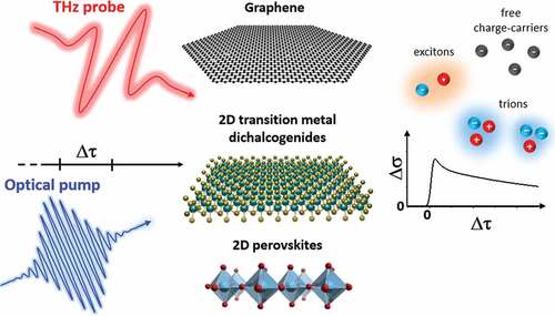
ABSTRACT
In this review, we discuss the rich ultrafast response at terahertz (THz) frequencies of two-dimensional (2D) materials. Thanks to their unique optoelectronic properties and exceptional tunability, van der Waals organic and inorganic 2D materials, such as graphene, transition metal dichalcogenides (TMDs), and 2D perovskites, are emerging as promising platforms for the development of nano-electronic and nano-photonic devices in the THz range. The investigation of the ultrafast charge carriers dynamics resulting from their reduced dimensionality is crucial for guiding the engineering route towards novel nanotechnologies. Here, we first give a brief overview of the state-of-the-art experimental schemes for inspecting the ultrafast response of 2D materials in the THz range, including the generation and the detection of THz light and the prototypical optical pump THz probe setup. Then, we present and discuss the most relevant results, reviewing the THz ultrafast signatures of charge carriers and excitons dynamics in graphene, TMDs, and 2D perovskites. Finally, we provide a vision of the emerging tools for characterizing the ultrafast THz dynamics at the nanoscale.
Graphical Abstract
1. Introduction
Since the discovery of graphene in 2004 [Citation1], 2D materials have become one of the most explored playgrounds for the ultra-scaling of devices for different applications [Citation2–4]. Layered 2D materials, such as graphene, hexagonal boron nitride (hBN), transition metal dichalcogenides (TMDs), and related van der Waals (vdW) heterostructures, have gained great attention as a promising platform for the development of THz photonic and optoelectronic devices [Citation5,Citation6], able to address, with innovative solutions, the high demand for reliable and practical THz technologies. 2D materials present distinctive, highly-tunable optical and electronic properties, support extreme light confinement, and ultrafast charge carriers dynamics, that can be exploited for the manipulation, propagation, generation, and detection of THz waves with an unprecedented level of control [Citation6].
The exploitation of light as a probe of new exotic phenomena in these emerging materials, gives access to delicate details of the physical processes under investigation. The comprehension of the fundamental mechanisms that govern the functionalities of 2D materials is a mandatory step toward their effective exploitation in practical devices. In this respect, ultrafast spectroscopy continuously increased its area of applications becoming one of the most explored characterization techniques for the study of extended as well as isolated systems, due to its capability to investigate physical effects with unprecedented details. In the last decade, time-resolved optical spectroscopy in the near-infrared (NIR) and visible (VIS) range, has been extensively applied to probe the transient response of 2D materials and related heterostructures, unveiling the effects of the strong enhancement of many-body Coulomb interactions that results from quantum confinement and reduced screening in 2D [Citation7,Citation8], testified by the large exciton binding energies (~hundreds meV) and the formation of multiparticle excitations, such as trions and biexcitons [Citation9]. In particular, time-resolved spectroscopy has allowed to observe large renormalization of the optical transition energies upon photoexcitation [Citation10,Citation11], to track the dynamical exciton response [Citation12–14], to probe the strong electron–phonon interaction [Citation15,Citation16], and many other non-linear processes (e.g. harmonics generation) in atomically-thin materials. In this framework, ultrafast spectroscopy in the THz range (1 THz = 300 µm = 4 meV) represents a powerful tool among the time-resolved techniques, as many fundamental excitations, in strongly-correlated electronic systems and nanoscale materials, occur at such low energies. Free carriers and electron-phonon related phenomena as well as low-energy collective oscillations of conduction charges, show their fingerprint in the THz spectral range. Moreover, by lying close to the Fermi level, the charge carriers that are photoexcited by THz waves are closely connected to DC transport. By detecting in the time domain, the amplitude and phase of a THz pulse that has interacted with the 2D material, its complex dielectric function, or complex conductivity, can be directly obtained, without the need for Kramers-Kronig relations. The access to the optical conductivity, combined with the time resolution that results from the short temporal duration of the THz time-domain sources, makes ultrafast THz spectroscopy the key spectroscopy technique for the study of fundamental physical phenomena occurring in 2D materials, where the dynamical response of free charges and bound quasiparticles, together with their interplay with the lattice, are strongly influenced by the dielectric landscape and quantum confinement.
In this review, we focus on the out-of-equilibrium THz response, investigated by optical pump – THz probe (OPTP) spectroscopy, of graphene, atomically thin TMDs, and 2D perovskites, which represent three prototypical classes of 2D materials. In section 2, we discuss different schemes for the generation and detection of THz pulses, the experimental configurations for measuring the charge-carriers dynamics, and the procedures routinely exploited to retrieve the pump-induced optical conductivity in the frequency domain from the THz fields acquired in the time-domain. In section 3, we discuss the most significant results concerning the charge carriers in graphene (section 3.1), and exciton dynamics in TMDs (section 3.2) and 2D perovskites (section 3.3). In the Perspective we discuss ultrafast THz nanoscopy as the emerging tool to enable the extension of ultrafast THz spectroscopy to the nanoscale, explore regimes of strong-light matter interaction and resolve spatial inhomogeneities in the THz response of 2D materials.
2. Ultrafast THz spectroscopy
2.1. Generation of THz radiation
THz radiation can be generated as continuous waveforms (CW) or broadband pulses. CW THz generation can be obtained by exploiting electronic sources, photomixing, and quantum cascade lasers (QCL) [Citation17]. In this review, we focus on the generation of broadband THz pulses that, in contrast with CW THz generation, requires the use of femtosecond laser sources and enable the investigation of ultrafast dynamics by time-resolved THz spectroscopy (TRTS).
The underlying idea is that the large bandwidth and the ultrashort duration of the driving pulse, provided by femtosecond lasers, can be leveraged to obtain transient electromagnetic fields with frequencies in the THz range. This is usually obtained following two different main strategies. The first one is inducing a transient current density of free charges, while the second one is inducing a transient polarization field in a crystal lattice [Citation18].
The first strategy can be accomplished by photoconductive (PC) antennas [Citation19] and this solution is typically employed when the laser system is an oscillator without any additional amplification stage. The reason is that PC antennas do not require high intensities to be operated. In fact, high pulse energies can easily damage them, unless some care is dedicated to choosing a PC antenna with a large enough aperture (and a correspondingly high bias voltage) or to adjusting the pulse energy of the generation beam below the damage threshold [Citation20,Citation21]. PC antennas represent also an attractive solution for the development of on-chip integrated THz systems [Citation22,Citation23].
A growing interest has been recently dedicated to an emerging class of THz sources called spintronic emitters [Citation24]. In these devices, based on layered heterostructures, the photoinduced spin-current in a ferromagnetic material is converted into a transient charge-current in a non-magnetic material. This conversion relies on the inverse spin Hall effect (ISHE).
Concerning the second strategy, based on polarization effects, the generation of THz radiation is typically obtained by exploiting non-linear processes in solids. In this case, high laser intensities are in general beneficial and, the handling conditions of solid-state emitters are usually less demanding, compared to those of PC antennas. For this reason, crystals are the most frequent choice to obtain THz pulses from amplified laser systems.
The working principle of solid-state emitters usually relies on optical rectification (OR). The THz bandwidth obtained by OR is mainly limited by phase-matching conditions and by the absorption in the crystal itself, due to the interaction with phonons in the relevant spectral range. A careful choice of the crystal is therefore critical to extend the bandwidth of the emitted THz pulse up to 10 THz and beyond.
THz generation by laser-induced plasma in air is currently a fairly common technique when a bandwidth of tens of THz needs to be explored. This technique was originally interpreted as four-wave mixing (FWM) rectification in laser-ionized air, due to the coupling of and
components by the third-order susceptibility
[Citation25,Citation26]. A different semi-classical model based on a transient current density of the ionized electrons was then demonstrated to better explain the process [Citation27,Citation28]. A further quantum mechanical model can be found in reference [Citation29].
2.1.1. Photoconductive antennas
A typical PC antenna [Citation30,Citation31], or PC switch, comprises an undoped semiconductive substrate and two metallic electrodes, lithographically fabricated on top of its surface. An ultrashort optical pulse photoexcites electrons to the conduction band of the substrate. In this way the PC switch is turned on and a DC bias voltage applied to the electrodes can drive a current density.
The temporal evolution of this current density is then determined by the recombination dynamics of the photo-excited free charge carriers. The acceleration of the charge carriers is responsible for the emission of radiation, consequently, the switch-on and recovery times determine the frequency range of the emitted pulse. A phenomenological model, clarifying the main physical aspects of THz generation in PC antennas can be found in reference [Citation32]. Monte Carlo simulations were also carried out in references [Citation33,Citation34].
The ultrafast dynamics of the transient current density is consequently responsible for the emission of a THz pulse and, to increase its bandwidth, the optical pulse duration and the recombination time must be as short as possible. For this reason, the most successful substrate operating at an excitation wavelength of 800 nm is made of low-temperature grown GaAs (LT-GaAs). The first PC antennas employed semi-insulating GaAs (SI-GaAs) or radiation-damaged silicon-on-sapphire (SOS). Low-bandgap materials like InGaAs and InGaAs/InAlAs heterostructures are currently attracting more interest, thanks to their higher absorption at the telecom wavelength 1.55 m.
The emitted THz pulse propagates in the substrate, it is then collected by a high-resistivity float-zone (HRFZ) silicon lens attached to the back of the antenna and eventually transmitted to free-space. The combination of the HRFZ silicon lens with an off-axis parabolic (OAP) mirror allows for obtaining a collimated THz beam.
2.1.2. Optical rectification
Optical rectification refers to the generation of a polarization with non-vanishing time-average inside a crystal interacting with intense laser beams [Citation35]. The non-vanishing time-average is due to the zero-frequency, or ”DC-component”, of the non-linear polarization. Thanks to this phenomenon, the transient electrical dipole induced by an ultrashort pulse inside a crystal can radiate a THz pulse. This can also be seen as a difference frequency mixing of the components within the spectrum of the ultrashort pulse.
Second-order optical rectification is usually the dominant contribution to the emission of THz radiation [Citation36], therefore it is convenient to use non-centrosymmetric crystals, where the second-order non-linear susceptibility is non-vanishing. The highest frequency of the emitted THz pulse is virtually limited by the bandwidth of the driving optical pulse, but in practice, the emitted bandwidth is cut off by the phase-matching conditions and by the absorption due to the phonon modes in the crystal itself.
Thanks to the good phase matching at 800 nm and the high second-order non-linearity, the most common crystal used for THz generation with Ti:Sa based laser systems is ZnTe. This crystal offers a bandwidth up to 3 THz, limited by the absorption by IR-active phonons in the crystal. The most straightforward way to extend the bandwidth is to use crystals with optical phonons lying at higher frequencies. A popular choice is GaP, which gives access to a larger bandwidth up to 7 THz [Citation37].
Another possibility is represented by thin GaSe crystals. If care is dedicated to meeting the correct phase-matching conditions, the generated radiation can be tuned in a frequency range approaching 100 THz [Citation38–40]. Efficient THz generation and large bandwidths can be also obtained by organic crystals like DAST, DSTMS and OH1 [Citation41]. These crystals often present a better phase-matching when pumped in the nm range [Citation21].
The generation of high-power THz pulses by optical rectification was also studied in organic crystals [Citation42] and in LiNbO3 [Citation43]. A pulse front tilting scheme is required in LiNbO3 to overcome the high-velocity mismatch between the 800 nm and the generated THz radiation [Citation44].
2.1.3. Laser-induced air plasma
This method relies on the ionization of molecules in the gas phase by a two-color laser pulse and allows to obtain a bandwidth of tens of THz. The asymmetric oscillation of the two-color electric field can induce a drift current of the ionized electrons and this is the main contribution to the emission of a THz pulse [Citation27,Citation45]. This is usually obtained by focusing the nm beam of a Ti:Sa laser through a thin BBO crystal (typically type I,
m-thick) for second harmonic generation (SHG). The generated 400 nm pulse can then interact with the residual 800 nm pulse at the beam waist, forming an intense two-color electric field.
The second harmonic and the fundamental pulse must be synchronized at the beam waist and it is important to maximize the polarization component of the 400 nm parallel to the polarization of the 800 nm [Citation26]. The relative orientation of the polarization can be optimized either by rotating the BBO around the normal direction to find a compromise with SHG efficiency [Citation28], or by using a dual-wavelength wave plate (DWP) [Citation46,Citation47]. Fine-tuning of the relative phase between the fundamental and the second harmonic is also necessary to maximize the generated THz field [Citation27]. Different gases and pressure values were also considered, demonstrating a further possibility to optimize the efficiency of the process [Citation28].
The generation of intense THz pulses by relativistic laser-induced plasma is also attracting increasing attention in recent years [Citation48]. This can provide unprecedented THz field strengths (>GV/m) and pulse energies ( mJ).
2.2. Detection of THz radiation
Time-resolved THz spectroscopy takes advantage of coherent detection techniques, or in other words, of the possibility of accessing both amplitude and phase information from the detected THz pulse. This enables the reconstruction of the complex response of the material under study, without the use of Kramers-Kronig relations. Some incoherent detection methods like Golay cells, pyroelectric sensors, and bolometers exist as well. These detectors can be also coupled to a Michelson interferometer to characterize the power spectrum of the THz pulse, similarly to what is done in Fourier-transform infrared spectroscopy (FTIR). Here, we are going to focus on coherent methods based on PC antennas, electro-optic crystals, and gas photonics.
PC antennas identical to the ones used for THz generation can be also used for THz detection. In this case, the electrodes are not biased by a constant voltage, because the THz electric field itself is responsible for the generation of a measurable photocurrent. This can flow only when free charge carriers are generated by an ultrashort gate pulse in the semiconductive substrate between the electrodes. The measured current is then proportional to the convolution of the THz electric field and the substrate transient photoconductivity [Citation38]. Consequently, it is possible to sample in the time-domain the waveform of the THz electric field, scanning the delay between the THz and gate pulses. The gate pulse and the lifetime of the photogenerated carriers determine the spectral sensitivity of the PC antenna.
The most common detection technique in time-resolved THz spectroscopy is electro-optic sampling (EOS). The electric field of the THz pulse can modify the polarization of an ultrashort optical pulse when these are overlapped in a crystal with a large second-order non-linear response. This can be related to the Pockels electro-optic effect and a complete frequency-domain description of its application for THz detection can be found in reference [Citation49].
The polarization-change is proportional to the THz field and can be measured by a lock-in amplifier, using an ellipsometry setup as explained in reference [Citation49]. The reconstruction in the time-domain of the full THz waveform is then obtained by scanning the delay between the THz and the gate pulse. The same crystals used for THz generation by OR can be used for THz detection with EOS. The absorption inside the crystal, the phase-matching conditions, and the walk-off limit the measurable bandwidth. Thinner crystals can be used to improve the detected bandwidth, at the cost of a smaller electro-optic signal, as a consequence of the shorter interaction length [Citation50,Citation51].
Coherent detection techniques based on gas photonics were also developed to obtain efficient broadband detection. The most common approach is called air-biased coherent detection (ABCD) [Citation52,Citation53]. The detection is based on the third-order coupling of the THz electric field with an ultrashort 800 nm gate pulse and an alternating external bias, applied between two electrodes at the focal point. This interaction generates a second harmonic (400 nm) signal, which is proportional to the THz field and can be measured by a photomultiplier tube (PMT).
2.3. Experimental configurations
shows a typical configuration for performing an OPTP spectroscopy experiment. An ultraviolet-visible (UV-VIS) or NIR light pulse ( eV) is used as a pump to photoexcite the sample generating a high-energy charge carriers distribution. The temporal evolution of the photo-excited charge carriers distribution, is then monitored by measuring the absorption of a second pulse, the probe, which is in the THz range (
meV). Probe detection can be performed in transmission or reflection geometry, depending if the substrate that supports the sample is semi-transparent or reflects the THz light. Common substrates for static transmission measurements on 2D materials include quartz, HR Si, SiC, sapphire, and many polymeric materials (such as polyethylene terephthalate, PET) [Citation54]. To perform OPTP experiments, the choice of the most suitable substrate is limited to those materials, which do not present a pump-probe signal.
Figure 1. Prototypical setup for OPTP spectroscopy experiments. An amplified laser system delivers fs pulses to the THz generation and detection arms and to the wavelength conversion setup exploited for exciting the samples. The two choppers (C1 and C2) modulate the THz generation and the pump pulses at different frequencies to obtain and
E
, respectively. Off-axis parabolic mirrors are exploited to collimate and focus THz radiation. Balanced photodiodes are used to acquire the signals that are demodulated at the relevant frequencies by a lock-in amplifier. The setup is enclosed in a purged N2/ dry air or kept in vacuum to remove THz absorption by water vapor. D1 and D2 are the delay stages used to control the pump-probe and EOS delay respectively.
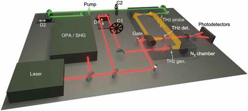
The relative time delay between pump and probe pulses is usually controlled by changing the path length of one of the two pulses, and the temporal resolution is determined by the time duration of the pump and probe pulses. In TMDs, the use of a circularly polarized pump allows for valley-selective excitation or detection. The spot size of the THz probe pulse in OPTP measurements is typically
1 mm imposing a limitation on the sample size and, accordingly, on the type of 2D material that can be investigated.
The pump beam is usually modulated by an optical chopper, so that a lock-in amplifier can be used to measure the pump-induced change of the THz field , where
and
represent the detected THz field with the pump beam on and off, respectively. The relative change of the probe can be evaluated by combining the differential signal
with an independent measurement of
, obtained by modulating the THz generation beam with a different chopper. The pump and generation beams can be also simultaneously modulated at different frequencies to obtain both the
and
signals with a single measurement, as explained in reference [Citation55]. In the cited article, the double modulation technique is proposed using a single chopper wheel, with two different sets of slots. The rotation speed of the chopper is such that the outer set modulates the pump beam at 500 Hz, while the inner one modulates the generation beam at 333 Hz.
The relations used in [Citation55] to compute the waveforms are here derived in a simple way, with the assumption of an instantaneous response of the photodetectors. In realistic modeling of the process, one has to take into account the temporal shape of the detected electric signal, which depends on the acquisition system, as well as on the actual modulation functions of the choppers at the two frequencies. Since all these signals are periodic in the temporal domain, they can be decomposed in the Fourier series with infinite contributions. However, the main mechanism behind the technique can be captured just by stopping these Fourier series to the first two terms, i.e. the CW and the fundamental frequency components. In this case, the current difference provided by the balanced photodetectors and sent to the lock-in amplifier at fixed pump-probe and EOS delays, can be represented by sinusoidal functions. In the absence of the pump beam the signal is written as a cosine function oscillating at 333 Hz :
When the pump beam, modulated at frequency 500 Hz, is photoexciting the sample, the THz probe pulses are modulated by the transient response of the material. The modulation function can be written in this framework as:
where the frequency of the modulation is 500 Hz = . Therefore, the signal sent to the lock-in amplifier can be modeled as
:
When the pump beam is blocked, we can take , therefore T = 1 and the lock-in demodulates at frequency
the amplitude
of the oscillation in EquationEquation (1)
(1) . When the pump beam is unblocked, we can demodulate two signals at different frequencies:
at frequency
and
at frequency
. Looking at EquationEquation (3)
(3) , we can conclude that the output given by the lock-in demodulators will be:
following Iwaszczuk et al., the effect of the non-instantaneous response of the photodetectors can be modeled by dividing EquationEquation (5)(5) by a calibration constant A, which can be experimentally determined. Since the output of the lock-in with the pump beam blocked is interpreted as the reference THz field, we can also take
,
,
and
to be consistent with the reference [Citation55]. Therefore, with these definitions, we find:
which are the relations used by Iwaszczuk et al. The differential signal is consequently given by .
Two different acquisition modes can be used. First of all, it is possible to keep a constant EOS delay and scan the pump-probe delay, obtaining the pump-probe dynamics . This acquisition mode gives frequency-averaged information about the THz probe pulse. The second possibility is to acquire a complete 2D map
, scanning both the EOS and the pump-probe delays.
Let us now introduce how the data are processed in a typical OPTP experiment in transmission geometry. The differential and pump-off
signals can be Fourier-transformed and used in this case to compute the transient transmission function of the sample
. The transmission function can be theoretically modelled and compared with the experimental data. The transient response function of the material can be then retrieved by different numerical approaches [Citation56–58]. When the photo-excited material can be considered a thin-film, as it is usually the case for samples of 2D materials, the photoconductivity is commonly directly related to the transient transmission function by the following relation [Citation59,Citation60]:
where and
are the real refractive indices of the media surrounding the thin-film,
is the thickness of the photo-excited material, and
is the impedance of free-space. When the photoinduced change is small, so that
, EquationEquation (8)
(8) is often replaced by the further approximated relation [Citation60,Citation61]:
The photoconductivity is related to the photoinduced change of the dielectric function by . Therefore, if the THz response of bound charges is changing because of the pump, this will also appear in the photoconductivity spectra [Citation58].
We now consider only the pump-induced change due to the free charge carriers. In the simplest case, the THz conductivity of the sample before and after the photo-excitation can be described by the Drude model with . With this assumption, the response of the free carriers is approximately the real frequency-independent conductivity
and EquationEquation (9)
(9) relates the optical pump-THz probe dynamics to the photoconductivity. We can also write an approximated relation for the photoconductivity, at the first order in the variations
and
:
where and
are respectively the mobility and the carrier density when the pump beam is off. If
is negligible with respect to the photogenerated carrier density
, as it typically happens in intrinsic semiconductors, EquationEquation (10)
(10) becomes
.
The applicability of these hypotheses must be always carefully evaluated because the role of bound charges and collective excitations can significantly complicate the physical interpretation of OPTP dynamics [Citation60,Citation62]. The most complete set of information can be retrieved by the frequency-resolved photoconductivity spectra.
3. Ultrafast THz response of 2D materials
In this section, we present a compendium of the most recent studies of charge carrier dynamics in 2D materials, including graphene and graphene-based heterostructures, TMDs, and 2D perovskites, as investigated by ultrafast THz spectroscopy. For graphene, the response to THz driving fields is dominated by the interaction with mass-less Dirac electrons, giving rise to strong non-linear response, mostly facilitated by intraband conductivity [Citation63]. In the following, we present the key experiments on graphene charge carrier dynamics, showing dependence on intrinsic (e.g. doping) and extrinsic parameters (e.g. defect, substrate), with a focus on the several results of OPTP that have significantly contributed to the understanding of graphene THz nonlinearity. For TMDs, OPTP spectroscopy revealed the free charges, excitons, and trions dynamics. Moreover, it allowed understanding of the impact of the growth conditions, e.g. the role of defects, substrate, and doping. For the 2D perovskites case, OPTP allowed observing the presence of excitons at room temperature and their interplay with the polaronic unbound carriers, confirming the exciton-polaron picture.
3.1. Graphene
Graphene is an elemental semimetal endowed with large electron mobility (>100000 cm2V–1s–1 [Citation64]), broadband optical absorption [Citation65], easily-tunable Fermi energy (up to
1 eV) by electrostatic gating, ensued by the linear dispersion of its conduction (CB) and valence (VB) bands, crossing at the Dirac points, at which there is a vanishing electron density of states [Citation66], see .
Figure 2. (a)Electronic band structure of graphene. Conduction and valence bands cross at six K points, at which they have linear dispersion relation forming Dirac cones, corresponding to the energy spectrum of massless Dirac fermions [Citation83]. (b) Calculated optical absorption of graphene as a function of the photon energy at different Fermi level/ sheet resistance R [Citation84]. (c) Broadband THz frequency-dependent conductivity of graphene measured with commercial and air plasma TDS systems and fit with Drude model of EquationEquation 12(12) (dashed black line), from Ref. [Citation54].
![Figure 2. (a)Electronic band structure of graphene. Conduction and valence bands cross at six K points, at which they have linear dispersion relation forming Dirac cones, corresponding to the energy spectrum of massless Dirac fermions [Citation83]. (b) Calculated optical absorption of graphene as a function of the photon energy at different Fermi level/ sheet resistance R [Citation84]. (c) Broadband THz frequency-dependent conductivity of graphene measured with commercial and air plasma TDS systems and fit with Drude model of EquationEquation 12(12) (dashed black line), from Ref. [Citation54].](/cms/asset/653b53a2-f6d9-40f5-98c3-2dd95952e1e1/tapx_a_2120416_f0002_oc.jpg)
Steady-state transport properties of graphene are controlled by charge carriers residing near the Fermi level, while, the transport in high-speed devices depends on higher-energy charge carriers, whose temperature is increased by the presence of dynamic external fields.
First studies of the relaxation dynamics of the charge carriers in single-layer graphene (SLG) were mainly driven by the scientific interest in the effect of reduced dimensionality on the electron–electron and electron–phonon interactions [Citation67–71]. More recently, the interest has multiplied by the emergence of highly promising optoelectronic applications exploiting the ultrafast dynamics of graphene carriers, such as ultrafast THz photodetectors [Citation72–75], high-speed large-bandwidth optical modulators [Citation76,Citation77], ultrafast THz saturable absorbers [Citation78,Citation79], efficient terahertz frequency multiplier [Citation80] and phase-shifters [Citation81,Citation82].
Light absorption in SLG is defined by the interplay of interband [Citation85,Citation86] and intraband [Citation87–90] electronic transitions, see . The first dominates in the VIS, NIR and mid-infrared ranges and can be described by the interband optical conductivity: [Citation91]:
where e is the electron charge, is the Boltzmann constant,
is the chemical potential and
is the charge-carriers temperature describing the Fermi-Dirac (FD) distribution of charge-carriers in SLG. For large photon energies (
)
reduces to
giving a frequency independent absorbance A
2.3% where
is the fine structure constant [Citation65].
At THz frequencies, interband transitions are usually inhibited by Pauli blocking since a SLG is always endowed with finite doping (>30 meV), i.e. 2
and intraband carrier transitions dominate [Citation92]. The intraband absorption
is well-described by the Drude model of a 2D electron gas [Citation93]:
where is the DC conductivity at
= 0 and
is the scattering time. The Drude weight D of graphene differs from that of conventional metals and semiconductors, being D =
with
the Fermi velocity and
the charge carrier density [Citation90,Citation94,Citation95] and
the Planck constant. A microscopic description of intraband optical conductivity can be found in Ref. [Citation96], where long-range Coulomb scattering with impurities is included in the calculation of the energy-momentum dependent scattering rate
. Semiclassical Boltzmann transport theory [Citation91] allows to extract
and the carrier mobility
from the
and
as follows [Citation54]:
Accordingly, THz spectroscopy measurements, in transmission and reflection mode [Citation54,Citation97], enables for a non-destructive characterization of the electrical properties of SLG, see .
The charge carrier dynamics in SLG has been extensively investigated using pump-probe techniques in which the charge carriers are brought out-of-equilibrium by impulsive excitation with an electrical or optical pulse, and, the equilibrium recovery is studied in the time-domain.
Impulsive excitation via interband absorption of femtosecond VIS or NIR pulses can be exploited to induce non-thermal distributions of charge carriers [Citation68,Citation69], peaked at half of the pump photon energy from the Dirac point, in the CB for electrons and the CV for holes. This first stage of the relaxation dynamics, needed by the carriers to assume FD distributions with defined temperature and a larger momentum spreading, is referred in the literature as thermalization. The subsequent decay through quasi-equilibrium states described in terms of a hot
is called cooling.
The thermalization occurs on sub-100 fs timescale, and it has been rationalized in terms of electron-electron Coulomb scattering processes [Citation68–70,Citation98], such as interband and intraband carrier-carrier scattering and Auger processes. The latter includes impact ionization or carrier multiplication, and the Auger recombination [Citation69,Citation70,Citation98,Citation99]. This ultrafast carrier heating was first observed by time-resolved ARPES by Gierz et al. [Citation70] in 2013, as a smearing of the electron FD distribution in the energy-momentum space. Interestingly, the thermalization is accompanied by hot carrier photoluminescence (HotPL) [Citation100–102], first discovered by Lui et al. [Citation103], due to the radiative recombination of the excited charge carriers emitting a broad spectrum extended from the VIS [Citation104] to the THz [Citation105] with a frequency-dependence resembling the emission of a gray body at temperature [Citation102,Citation103], see .
Figure 3. (a-c) Schematic illustration of the HotPL emission mechanism in n-doped SLG from Ref. [Citation102]. Dirac cones populated by e (red)-hole (h,blue) with thermal distribution at T0 at the equilibrium (a); out-of-equilibrium charge distributions formed within 20 fs after ultrafast laser excitation (b), thermalized e-h distributions at >T0 with two different chemical potentials formed on a time scale comparable with the pump pulse duration leading to radiative electron-hole recombination, i.e. HotPL, restoring the initial equilibrium h density (c). (d) HotPL spectrum at different Te from Ref. [[Citation103]].(e-f) Photoinduced change in the THz transmission through graphene (e) and inferred change in the graphene conductivity (f) from Ref.[Citation106] [].(g) Temporal evolution of the change in the maxima of the transmitted THz waveforms normalized by the THz probe for different pump fluences [Citation106]. The inset shows the decay times extracted by fitting the dynamics with single exponential function. Panels e-g are reprinted with permission from Ref.[Citation106]. Copyright {2022} American Chemical Society.
![Figure 3. (a-c) Schematic illustration of the HotPL emission mechanism in n-doped SLG from Ref. [Citation102]. Dirac cones populated by e (red)-hole (h,blue) with thermal distribution at T0 at the equilibrium (a); out-of-equilibrium charge distributions formed within 20 fs after ultrafast laser excitation (b), thermalized e-h distributions at >T0 with two different chemical potentials formed on a time scale comparable with the pump pulse duration leading to radiative electron-hole recombination, i.e. HotPL, restoring the initial equilibrium h density (c). (d) HotPL spectrum at different Te from Ref. [[Citation103]].(e-f) Photoinduced change in the THz transmission through graphene (e) and inferred change in the graphene conductivity (f) from Ref.[Citation106] [].(g) Temporal evolution of the change in the maxima of the transmitted THz waveforms normalized by the THz probe for different pump fluences [Citation106]. The inset shows the decay times extracted by fitting the dynamics with single exponential function. Panels e-g are reprinted with permission from Ref.[Citation106]. Copyright {2022} American Chemical Society.](/cms/asset/de843ab0-f938-4b76-9c6b-4d77e67c1384/tapx_a_2120416_f0003_oc.jpg)
The cooling of the hot thermalized charge carriers has been studied by OPTP spectroscopy [Citation71,Citation96,Citation106–112] which allows following the time-evolution of as an ultrafast electron thermometer, monitoring the induced modifications to the THz absorption. In intrinsic graphene (
0.1 eV), the ultrafast photoexcitation produces an increase of the THz conductivity, as expected for a semiconductor after interband photoexcitation. In doped graphene (
0.1 eV), instead, a reduction in the THz conductivity was observed by several groups [Citation71,Citation96,Citation106,Citation110,Citation111,Citation113], detected in transmission geometry as a transmission increase
0, that scales roughly linearly (or weakly sub-linearly) with the change
in the temperature of the charge-carrier distribution. The negative THz photoconductivity, which indicates that the ultrafast interband excitation makes doped graphene more resistive to THz fields, was explained in terms of hot-carrier multiplication [Citation71,Citation96,Citation114], i.e. the scattering of photoexcited electrons with the background electrons in the Fermi sea which increases their energy. This electron-electron scattering has a rate that can largely exceed that of electron-phonon scattering and is related to the ultrafast thermalization processes producing the increase of
by supporting fast energy and momentum exchange within the entire electron population.
The ultrafast electron transport in graphene, on timescales longer than that of the thermalization, is described considering time-dependent quasi-equilibrium within the electron population, using a thermodynamic model of the conductivity [Citation96,Citation115,Citation116]. Charge carrier heating can be induced also by intraband excitation with strong THz fields acting on the free carriers in the vicinity of the Fermi level [Citation115,Citation117]. Since the thermalization is much faster than the duration of the THz field cycle, the THz energy is quasi-instantaneously converted into the thermal energy of the electron population, which is simply described by its instantaneous temperature , which accumulates during the THz field oscillation as shown in .
Figure 4. (a) The calculated time-dependent in graphene during the interaction with the THz fields in the range 2.3–120 kVcm–1 compared to the absolute value of the experimentally measured ultrafast electric field transient as a gray area, from Ref. [Citation115]. (b) Sketch of the evolution of the FD distribution (fD) and charge carrier population Ne with Te, T* T0, from Ref. [Citation116], in case of adherence (dashed red solid line) or violation (solid red line) of particle number conservation, implying constant or down-shifted chemical potential, respectively. (c) Change in the complex-valued conductivity spectrum of doped graphene with
in case of spectral weight conservation, from Ref. [Citation116].
![Figure 4. (a) The calculated time-dependent in graphene during the interaction with the THz fields in the range 2.3–120 kVcm–1 compared to the absolute value of the experimentally measured ultrafast electric field transient as a gray area, from Ref. [Citation115]. (b) Sketch of the evolution of the FD distribution (fD) and charge carrier population Ne with Te, T* T0, from Ref. [Citation116], in case of adherence (dashed red solid line) or violation (solid red line) of particle number conservation, implying constant or down-shifted chemical potential, respectively. (c) Change in the complex-valued conductivity spectrum of doped graphene with in case of spectral weight conservation, from Ref. [Citation116].](/cms/asset/9b65ba6d-9c56-4129-a686-3e54e278ce18/tapx_a_2120416_f0004_oc.jpg)
The carrier heating must obey the conservation of carrier density, which implies that the chemical potential decreases with increasing Te while the FD distribution broadens, as depicted in . The downshift of the chemical potential, in turn, causes an increase in the number of optically active interband transitions at energies 2
and explains the reduction of intraband conductivity due to conservation of the total spectral weight, as sketched in . The heating efficiency per photoexcitation energy
has been evaluated in Ref. [Citation108] as
with
corresponding to the heat absorbed by the electron bath, and varies with the excitation fluences, from 1, standing for total energy conversion, to an asymptote of
approached at high fluences due to the competition with energy dissipation channels such as the optical phonon emission [Citation108].
The combination of the reduced THz absorption due to the highly efficient THz-induced carrier heating, and the ultrafast heating/cooling dynamics of hot electrons, results in an intense nonlinear response of graphene at THz energy which allowed observing THz harmonics with multicycle THz pulse [Citation118].
Hot charge carriers cooling proceeds via energy transfer to the lattice through the emission of strongly coupled optical phonons (SCOP) till a common temperature is reached. Then, the thermalized electron-optical phonon bath relaxes via anharmonic coupling to the acoustic phonons.
Optical phonons emission requires minimum excess energy, corresponding to G Raman mode (wavevector q = 0, 1560 cm–1, equivalently
meV) [Citation15] of the lowest-energy optical phonon branch, and it can involve either intraband transitions causing the electrons to cascade down to Dirac point, or electron–hole recombination or intervalley scattering by zone boundary phonons. Despite this energy constraint, this cooling channel is rather efficient thanks to the continuous re-thermalization of the electronic system through carrier-carrier scattering, which guarantees the presence of carriers with enough energy to emit optical phonons [Citation112,Citation119], see .
Figure 5. (a) Schematic overview of the hot-carrier relaxation channels in graphene including the thermalization to hot FD distributions, hotPL, cooling via emission of optical phonons anharmonically coupled with acoustic phonons, near-field coupling to the substrate phonons, from Ref. [Citation120]. b)Schematic illustration of electron relaxation via supercollision cooling with acoustic phonons without (left) and with (right) disorder, where the presence of disorder supports the emission of finite momentum qd acoustic phonons, from Ref. [Citation121]. Panel a is reproduced from Ref. [[Citation120]] with permission from the Royal Society of Chemistry.
![Figure 5. (a) Schematic overview of the hot-carrier relaxation channels in graphene including the thermalization to hot FD distributions, hotPL, cooling via emission of optical phonons anharmonically coupled with acoustic phonons, near-field coupling to the substrate phonons, from Ref. [Citation120]. b)Schematic illustration of electron relaxation via supercollision cooling with acoustic phonons without (left) and with (right) disorder, where the presence of disorder supports the emission of finite momentum qd acoustic phonons, from Ref. [Citation121]. Panel a is reproduced from Ref. [[Citation120]] with permission from the Royal Society of Chemistry.](/cms/asset/3913ef7a-2c79-43c9-8c2e-fb78ec8e0c2c/tapx_a_2120416_f0005_oc.jpg)
The direct coupling of the hot electronic system to acoustic phonons is in principle an inefficient cooling channel, which would lead to hundreds of picoseconds recovery time, due to the moment conservation constraints limiting the interaction to low-energy acoustic phonons with momentum , with the Fermi momentum
. However, defects or disorder can mediate the scattering with high-energy acoustic phonons providing the required extra momentum. The disorder-assisted scattering is referred to as supercollision cooling which is expected to be especially relevant for carriers near the Dirac point and in high-disorder low-electrical mobility graphene [Citation121,Citation122], see .
Following Ref. [Citation121], which is based on the theory developed in Ref. [Citation123], the supercollision cooling time can be estimated as , where
is the lattice temperature, and
. Here the mean free path is
, with the momentum scattering time given by
, and
, where
is the mass density,
is the sound velocity and
is the electron-phonon deformation potential which can be determined by transport measurements assuming phonon-limited momentum scattering [Citation124]. Accordingly, supercollision theory predicts a decrease in the cooling time for increasing defects density, as it has been observed by NIR pump-probe spectroscopy on SiO2-supported graphene [Citation125]. Currently, there are contrasting views in the literature regarding supercollision theory with some studies, such as Ref. [Citation126] questioning its role.
3.1.1. Graphene-based heterostructures
Graphene deposited on standard SiO2 presents a high degree of crystal disorder. Charge carriers scattering with impurities, defects and SiO2-optical phonon reduces the carrier mobility. Moreover, graphene tends to conform to the silicon oxide substrate forming strong spatial perturbations which have been observed by scanning tunneling microscopy [Citation127]. Charged impurities trapped in the substrate or at the graphene/substrate interface result in an effective p- or n-doping. OPTP measurements revealed that in high-quality ( 10 000 cm2V–1s–1) suspended graphene [Citation112] the charge-carrier relaxation is dominated by the cooling through optical phonons, which is more efficient than disorder-assisted supercollision cooling for which a much slower cooling time (
ps) is predicted.
Encapsulation with different dielectric materials has been proposed to preserve the superior properties (i.e. high-quality graphene with mobility as large as cm2V–1s–1 and low intrinsic doping) of suspended graphene without losing the advantages of having a substrate. Among the different encapsulants, hexagonal boron nitride (hBN) has been identified as a promising candidates being an isomorph of graphite with a small lattice mismatch (
= ahBN/agraphene = 1.8% [Citation127]), transparent to VIS and NIR thanks to the large electronic gap (
eV). Furthermore, due to the strong ionic nature of the in-plane bonding, it is relatively inert and free of dangling bonds and surface charge traps. Its surface is planar on the atomic scale and suppresses graphene rippling reducing the charge carrier scattering induced by surface roughness.
The hot electrons cooling in hBN-encapsulated graphene has been investigated by several techniques, including transport [Citation128], time-resolved photocurrent, NIR-transient absorption and OPTP [Citation129]. These studies demonstrate the appearance of an additional relaxation channel: the near-field coupling of the graphene charge carriers with the hyperbolic phonons (HP) of hBN whose theoretical definition is provided in Ref. [Citation130]. HP in hBN have mid-infrared energies ( 110 and 140 meV) and are associated with large phonon densities boosting the hot electrons cooling dynamics by supporting a very efficient Super-Planckian out-of-plane heat transfer [Citation129,Citation130].
To suppress the hyperbolic cooling and obtain longer-living charge carriers excitation, the encapsulation with thin films of TMDs, which have reduced hyperbolicity [Citation112] compared to hBN, has been proposed. High-quality devices with mobility up to 100 000 cm2 V–1 [Citation131] have been obtained using WSe2. However, the cooling dynamics of high-quality graphene is intrinsically limited by the relaxation via emission of SCOPs, which dominates the cooling when competitive channels are suppressed, imposing cooling time of few picoseconds. Similar dynamics have been observed by OPTP measurements in suspended high-quality graphene [Citation112] where interaction with the substrate is inherently excluded, see .
Figure 6. (a) hBN encapsulated graphene showing near-field energy transfer from hot electrons to the encapsulant explaining the observed picosecond OPTP dynamics, from Ref. [Citation129].(b) Calculated dielectric constants of hBN (blue lines) and WSe2 (red lines) along the in-plane directions (xx and yy, solid lines) and along the c-axis (zz, dashed lines) showing reduced hyperbolicity, from Ref. [Citation112]. (c) OPTP dynamics of suspended graphene from Ref. [Citation112]. Further permission related to the material excerpted to produce panels b-c, should be directed to the ACS.
![Figure 6. (a) hBN encapsulated graphene showing near-field energy transfer from hot electrons to the encapsulant explaining the observed picosecond OPTP dynamics, from Ref. [Citation129].(b) Calculated dielectric constants of hBN (blue lines) and WSe2 (red lines) along the in-plane directions (xx and yy, solid lines) and along the c-axis (zz, dashed lines) showing reduced hyperbolicity, from Ref. [Citation112]. (c) OPTP dynamics of suspended graphene from Ref. [Citation112]. Further permission related to the material excerpted to produce panels b-c, should be directed to the ACS.](/cms/asset/e7925cb2-9081-479d-b373-569f0996c6b1/tapx_a_2120416_f0006_oc.jpg)
In high-quality graphene, diffusive cooling becomes competitive with optical phonon emission as an additional relaxation channel [Citation132] that however is observed only with m size pump and probe spots.
3.1.2. Gate-tunability
By tuning the chemical potential via electrostatic gating, below or above the half frequency of impinging radiation, large tunability of the static and transient [Citation133] interband absorption of graphene has been demonstrated in the VIS and NIR.
At THz frequencies, modulation of the charge carrier density using either electrostatic gating or optical excitation allows for achieving large tunability of the intraband absorption (.
OPTP measurements as a function of , revealed that the THz photoconductivity of graphene can be continuously tuned from semiconductor-like positive values, displayed at near-zero carrier density reached at gate voltage
, to metal-like negative values at high carrier densities [Citation110,Citation111,Citation134], see .
Figure 7. (a) Sketch of the OPTP experiment on gated SLG, where the differential transmission of a THz probe pulse is investigated as a function of the Fermi level controlled by field-effect with a gate voltage [Citation110]. (b) Temporal evolution of the change in the THz field transmission
, proportional to SLG differential conductivity
, as a function of the Fermi energy
. (c) Instantaneous
signal at zero pump-probe delay showing the change of sign as increasing the doping from the charge neutrality point (
=0). The corresponding change in THz conductivity
is shown at the right axis. Panel a is adapted from Ref. [Citation110]. Panels b-c are adapted with permission from Ref. [Citation111] Copyright {2022} American Chemical Society.
![Figure 7. (a) Sketch of the OPTP experiment on gated SLG, where the differential transmission of a THz probe pulse is investigated as a function of the Fermi level controlled by field-effect with a gate voltage [Citation110]. (b) Temporal evolution of the change in the THz field transmission , proportional to SLG differential conductivity , as a function of the Fermi energy . (c) Instantaneous signal at zero pump-probe delay showing the change of sign as increasing the doping from the charge neutrality point (=0). The corresponding change in THz conductivity is shown at the right axis. Panel a is adapted from Ref. [Citation110]. Panels b-c are adapted with permission from Ref. [Citation111] Copyright {2022} American Chemical Society.](/cms/asset/ba5e43f6-d5a2-406b-8347-8b2abd971f3f/tapx_a_2120416_f0007_oc.jpg)
The multiple sign change in the THz photoconductivity (see , has been related [Citation110] to the temperature-dependence of the Drude weight and of the scattering rate , see ). It was shown [Citation96] that the ultrafast electronic thermalization in photoexcited undoped graphene (
0.1 eV), can also lead to free carrier multiplication via interaction with the VB states, in addition to the hot carrier multiplication, which instead preserves the total number of free carriers. Carrier multiplication was first predicted by Winzer et al. [Citation135], observed by Plötzing et al. [Citation136] and rationalized in terms of electron kinetics by Tomadin et al. [Citation96].
The doping allows also to tune the fluence dependence of the signal, exploiting the variation of the -dependence of the electronic heat capacity, which is quadratic at the charge-neutrality point CNP and becomes linear at high doping [Citation111].
The conversion efficiency of THz third-harmonic generation [Citation137] can be controlled by electrostatic gating exploiting the dependence of electronic heat capacity on doping. The THz nonlinearity of graphene has been indeed attributed to the collective thermodynamic response of free-carriers to the THz field. Increasing the free carriers, i.e. , enhances the power absorption leading to an increasing nonlinearity, scaling approximately with the square of
. However, the THz-induced electronic temperature rise, decreases with increasing doping because the absorbed THz energy is shared among a very large number of carriers, diminishing the material’s thermodynamic nonlinearity. Accordingly, there is an optimal doping to enhance graphene’s THz nonlinearity [Citation137].
3.2. Transition metal dichalcogenides
Atomically thin TMDs are inorganic 2D crystals emerging as novel quantum materials, that, differently from graphene, exploit a direct band gap to conduct electricity whenever the electrons absorb enough energy through heat, light, and other means, therefore promising groundbreaking impacts in nano-electronics and nano-photonics. In analogy with graphite, TMDs can be easily thinned down to one atomic layer using mechanical as well as chemical exfoliation techniques. Moreover, they can be synthesized as single and multilayers with bottom-up approaches like Chemical Vapour Deposition (CVD) and Metal-Organic Chemical Vapour Deposition (MOCVD) techniques. At the single-layer limit, the physical properties of TMDs are dominated by the Coulomb interaction between the carriers resulting from the reduced dielectric screening and strong quantum confinement. Therefore, in contrast with other inorganic semiconductors, a single layer of TMDs shows a rich and robust exciton population at room temperature that promotes them as one of the most explored classes of materials for beyond state-of-the-art (opto)electronics. Both geological and synthesized TMDs are naturally doped, with the consequent electron/hole excess that has a sizeable impact on their electronic and optical properties.
Ultrafast THz spectroscopy emerged as a powerful technique to study the carrier dynamics in monolayer and few-layers TMDs, thanks to its peculiarities. The THz probe strongly couples to charged particles like free carriers and intra-exciton transitions as far as the probe photon energy matches some allowed 1s bright to np dark states transition [Citation138,Citation139]. When these transitions are not accessible by the probe bandwidth or cannot be resolved at room temperatures, it is still possible to obtain an indirect signature of the presence of the excitons in the THz transient photoconductivity. Indeed, bound e-h pairs induce a negative Im due to the exciton dielectric polarization and the related capacitive response [Citation140,Citation141].
As mentioned in Sec. 1, THz spectroscopy can access the complex photoconductivity spectrum by acquiring the entire waveform of the THz electric field at different pump-probe delays. Alternatively, it is possible to obtain the frequency-averaged real and imaginary photoconductivity by measuring the change of two special points of the THz waveform, as a function of the pump-probe delay. One point is the peak of the electric field, which is sensitive to amplitude variations and is slightly affected by small phase changes. A pure amplitude change is given by the low-frequency response of a photoexcited free-carrier gas. Therefore, in the absence of a large temporal shift induced by the pump, the dynamic of the peak reflects the conductive response (current in phase with electric field) of the sample and it is routinely described as the frequency-averaged real part of the photoconductivity. The other point is the zero-crossing, which is sensitive to phase shifts but not to amplitude variations. A phase shift can be induced by the polarizability of an exciton population [Citation141], which is related to a positive change of the real dielectric function and a correspondingly negative change of the imaginary photoconductivity. For this reason, the dynamics of the zero-crossing point reflects the capacitive response (polarization in phase with the electric field) and it is routinely described as the frequency-averaged imaginary part of the photoconductivity [Citation62].
Molybdenum Disulphide (MoS2) has been the most studied TMD, since the observation of the enhancement of the PL emission and the crossover from indirect to a direct band gap in the limit of the single monolayer [Citation142]. Concerning the carrier and exciton dynamics, a debate started after the observation of trion, a three-bodies quasiparticle formed by two electrons (holes) and one hole (electron), in the optical response of monolayer MoS2 [Citation143].
C. H. Lui and coworkers in their seminal work exploited OPTP spectroscopy to investigate the THz dynamic response of CVD grown monolayer MoS2 [[Citation144]]. The top panels of show the THz probe electric field in the time domain together with a sketch describing the pump-probe experiment. The bottom panels report an unexpected positive pump-induced THz response that would mean a persistent decrease of the conductivity of the material after the photo-injection of additional charge. In details, the bottom left panel shows a 150 ps long positive (
) composed by a short (
ps) and long (
ps) component, while the transient conductivity spectra reported in the bottom right panel shows negative real (Re(
) and imaginary (Im(
) parts. This counter-intuitive response observed regardless of the temperature (
K) and the fluence (
J
cm2), was explained by considering the presence of a doping-induced extra charge in the pristine monolayer that couples with the photo-generated el-h pairs forming negative trion (two electrons and one hole). The effective mass m
of this quasiparticle is higher as compared to the one of the unexcited material with the consequent decrease of the carrier mobility
. From EquationEquation 10
(10) , it follows that the transient response
becomes negative in presence of heavier carriers in the photo-excited material.
Figure 8. (a) The THz electric fields exploited as probe and (b) a sketch of the OPTP experiment; (c) and (b) the frequency-averaged and frequency-resolved pump induced THz response of monolayer MoS2, respectively (adapted from Ref. [Citation144]).
![Figure 8. (a) The THz electric fields exploited as probe and (b) a sketch of the OPTP experiment; (c) and (b) the frequency-averaged and frequency-resolved pump induced THz response of monolayer MoS2, respectively (adapted from Ref. [Citation144]).](/cms/asset/aff46834-f136-4b80-a16d-8cea05d226f2/tapx_a_2120416_f0008_oc.jpg)
The attribution of the negative conductivity to trion has been confirmed by exploiting different pump photon energies in OPTP experiments. When the pump photon energy falls below the A excitonic resonance, neither free carriers nor excitons can be generated in the material, and the THz response is totally quenched. As the pump photon energy approaches the A exciton, then the formation of exciton occurs and THz response sharply increases, in the absence of photo-generated free carriers. As the THz probe cannot couple with charge-neutral species and intra-exciton transitions lie at much higher energy with respect to the meV probe used for the experiments, the resulting negative THz dynamics can be solely ascribed to the presence of a charged exciton, i.e. the trion. In [[Citation144]] the authors further confirmed this claim by tuning the doping of the pristine monolayer. Remarkably, the effect of the p doping, which reduces the initial free charge, is the suppression of the trion formation, while n doping partially restores the pristine monolayer PL and THz dynamic response. These results support that trions form from the coupling of the doping-induced charge with the photo-generated e-h pairs population.
Although strong evidence supports the picture developed in [[Citation144]], C. J. Docherty et al. observed a different ultrafast THz response for a CVD grown monolayer MoS2. In particular, in [Citation145] a positive transient THz conductivity (, see EquationEquation10
(10) ) has been reported, with a signal that recovers within hundreds of fs with a simple exponential decay, regardless of resonant or non-resonant photo-excitation, suggesting that monomolecular processes are at play. Doping and fluence-dependent measurements allowed to assign of the fast recombination to trap-assisted processes at the surface due to the presence of a trap density higher than
cm–2. The frequency-resolved transient conductivity spectra reported in confirm the differences observed in the frequency-averaged THz response. In [Citation145] indeed, the authors observed a positive Re
accompanied by a negative Im
. This behavior typically occurs when a restoring force acts on the photo-generated free carriers, or when the probe photon energy matches a resonance, such as phonons, plasmons, or excitons. In this respect, trions in monolayer MoS2 have a binding energy of
meV (
THz) that falls in the
THz (
meV) spectral range of the probe used in [Citation145]. Therefore, J. C. Docherty et al. fitted the
with a Drude-Lorentz model, where an oscillator at
THz (15 meV) is needed to account for the trion resonance and the Drude term accounts for a small fraction of free charges. For the trilayer MoS2, J.C. Docherty et al observed a similar response but with the resonance located at much higher energy outside the THz probe region. As the trion is expected to occur for the monolayer only, this resonance can be related to excitons only. For the trilayer, the exciton binding energy is
meV (15 THz) and matches the dominant 1s-2p intra-excitonic transition [Citation146], thus inducing the Lorentz lineshape for the
.
Figure 9. (a) Top and bottom panels reports the photoconductivity of monolayer and trilayer MoS2, respectively (adapted with permission from Ref. [Citation145]). (b) Frequency-averaged (top-right and bottom-left panel) and frequency-resolved (bottom-right panel) photoconductivity of monolayer MoS2 adapted with permission from [Citation147].
![Figure 9. (a) Top and bottom panels reports the photoconductivity of monolayer and trilayer MoS2, respectively (adapted with permission from Ref. [Citation145]). (b) Frequency-averaged (top-right and bottom-left panel) and frequency-resolved (bottom-right panel) photoconductivity of monolayer MoS2 adapted with permission from [Citation147].](/cms/asset/2df72346-fb1b-4c7c-b3e5-6553c1666c74/tapx_a_2120416_f0009_oc.jpg)
In 2016, P. D. Cunningham et al. investigated CVD grown monolayer MoS2 with OPTP in the THz spectral region [Citation147]. Here the authors observed an increased photo-conductivity with an hundreds of fs dynamics similar to the one reported in [Citation145] (see the top-right panel of ), but sizeable differences in the conductivity spectra, i.e. a positive Re
with an almost negligible Im
(see bottom-right panel of ). This outcome points to a free-carrier dominated conductivity, and the deviation from a pure Drude dispersion has been ascribed to carrier back-scattering at defects or grain boundaries where random disorder causes destructive interference among carrier scattering events. This leads to a non-Drude conductivity that can instead be described by the phenomenological Drude
Smith model [Citation148]. The authors suggested that the absence of the signature for the trions, i.e. the negative photo-conductivity and the resonance at
meV, can be explained by considering the oxygen neutralization of the n
type doping at the grain boundaries.
The striking differences observed in the dynamical THz responses suggest that the parameters adopted for the CVD growth of monolayer MoS2 play a crucial role in determining the morphology and the doping level of the material. These in turn influence the formation of trions. Another detrimental aspect is the role of the substrate and the capping layer if present. Indeed, they determine the dielectric landscape for the monolayer and consequently the exciton and trion binding energies.
For the multi-layer case, the ultrafast THz dynamics of a chemically exfoliated free-standing MoS2 laminate consisting of layers were studied by S. Kar et al. In [Citation149] the authors performed a fluence-dependent study and analyzed the frequency-averaged THz response of the sample. The authors interpreted the results by developing a system of rate equations incorporating defect-assisted Auger scattering of photo-excited electrons, holes, and excitons. The dynamics of the laminate resulted to be composed of a fast (
ps) and a slow (hundreds of ps) relaxation channel. It emerged that defect states are used on a sharing basis by the free carriers as well as the excitons in relaxation kinetics. The rate coefficients of the free carrier and exciton capture obtained by the fit of the dynamics with the solutions of the rate equations were almost comparable and excitons bound to defects emerged to have a slower relaxation with respect to the free charge.
Concomitantly with the work of C. H. Lui et al. on the monolayer, J. H. Strait et al. presented their ultrafast THz investigation of bulk MoS2 [Citation150]. In this work, the authors performed OPTP spectroscopy to study the carrier mobility and the dynamics associated with carrier relaxation. Here, by varying the temperature in the K range, a free-carrier like THz conductivity was observed. From the fit with the Drude model, the authors extracted carrier mobility of
cm2V–1s–1 at 30 K. From the temperature dependence of the scattering time, they found how the mobility is intrinsically limited by acoustic phonon scattering below 200 K, while at the higher temperature the contribution of optical phonon becomes evident. Concerning the carrier recombination, by varying the fluence and fitting the dynamics with the solutions of a system of rate equations, the authors obtained that the carrier relaxation is characterized by a picosecond cooling time followed by recombination lasting tens of nanoseconds mainly attributed to Auger scattering into defects.
In the family of TMDs, the carriers and excitons ultrafast dynamics of CVD grown layers WS2 laminate ha been investigated using OPTP spectroscopy. In [Citation151], the authors reported the methodology adopted to disentangle the free carriers and exciton contributions. As summarized in the introduction of this section, by following the peak and the zero-crossing points it is possible to grab the bound and unbound carrier contributions to the frequency-averaged complex photoconductivity (see ). In this case, a restoring force provided by the excitons was also proposed as the origin of the localization of the unbound carriers. shows the frequency-averaged Re(
) and Im(
), both characterized by a 4 ps formation time that is, the concomitant ultrafast formation of free carriers and excitons, respectively. Remarkably, the relaxation dynamics of the Im(
) emerged to be much faster than the Re(
), suggesting that excitons recombine faster than free carriers. As shown in , Re(
) was fitted with a tri-exponential curve which describes the contribution of el-ph scattering (
ps), many-body effects (
ps), unbound el-h recombination
ps. An offset has been also included in the model to consider mid-gap trap-assisted processes (1 ns). The relaxation dynamics of Im(
) were conversely fitted with a bi-exponential curve that returns two fluence-independent decay times of
ps and
ps assigned to exciton-phonon coupling and exciton lifetime, respectively (see ).
Figure 10. (a) Reference (black curve) and the pump modulated (red curve) electric fields in the time-domain. The vertical dashed lines lie at those points in the time domain used to acquire the frequency-averaged real (peak of the electric field) and imaginary (zero-crossing point) photoconductivity. (b) Pump-probe scans were performed at the peak and at the zero-crossing points. (c) and (d) Fluence-dependent scans of the real and imaginary photoconductivity of WS2, respectively [Citation151].
![Figure 10. (a) Reference (black curve) and the pump modulated (red curve) electric fields in the time-domain. The vertical dashed lines lie at those points in the time domain used to acquire the frequency-averaged real (peak of the electric field) and imaginary (zero-crossing point) photoconductivity. (b) Pump-probe scans were performed at the peak and at the zero-crossing points. (c) and (d) Fluence-dependent scans of the real and imaginary photoconductivity of WS2, respectively [Citation151].](/cms/asset/b61ac18e-40c9-4a8e-a723-75c54eb6cda8/tapx_a_2120416_f0010_oc.jpg)
The frequency-resolved transient THz conductivity of WS2 shown in returns a Drude-Lorentz response, in analogy with the MoS2 laminate case, where the authors added an oscillator to the fit function to follow the negative Im(). While for MoS2 the Lorentz line-shapes were directly attributed either to trion or exciton resonances, for WS2 X. Xing et al. invoked a restoring force acting on the free carriers induced by the exciton polarization field as the origin of the charge localization.
Figure 11. (a) Photoconductivity of multilayer WS2 obtained with (left panel) different fluences and at (right panel) different pump-probe delays (adapted with permission from [Citation151]). (b) Photoconductivity of monolayer WS2 acquired at different pump-probe delays in the THz spectral range (adaptedwith permission from [Citation152]).
![Figure 11. (a) Photoconductivity of multilayer WS2 obtained with (left panel) different fluences and at (right panel) different pump-probe delays (adapted with permission from [Citation151]). (b) Photoconductivity of monolayer WS2 acquired at different pump-probe delays in the THz spectral range (adaptedwith permission from [Citation152]).](/cms/asset/d43639cd-18e5-4622-a8c2-5241b4acda92/tapx_a_2120416_f0011_oc.jpg)
For the monolayer WS2, the ultrafast THz response of CVD-grown samples has been investigated and the results have been published in 2019 by S. Xu et al. and J. K. Gustafson et al. [Citation152,Citation153].
In Ref. [Citation153] the first measurement of the THz photo-conductivity of monolayer WS2 is reported. Here the authors, from the fit with a bi-exponential curve of the 15 ps long dynamics, obtained fast (hundreds of fs) and slow (few ps) components assigned to charge carrier loss induced by the exciton formation and Auger recombination plus surface trapping, respectively. The THz conductivity spectrum reported by S. Xu et al. shows a positive Re() accompanied by a small but negative Im(
), which points to a free carriers conductivity. The authors fitted this spectrum at different delays with the Drude
Smith model and obtained a localization parameter of
, which indicates a relevant localization of the free carriers at the grain boundaries of the CVD-grown materials. The author also argued that the influence of excitons through their polarization field cannot be ruled out; however, if this were the case, the Drude
Smith model should have returned a c parameter around
, which would have led to a shape identical to the Lorentz oscillator.
In Ref. [Citation152] the authors performed ultrafast THz spectroscopy of monolayer WS2 at 20 K with a probe pulse covering the THz spectral region and with pump photons resonant and non-resonant with the A exciton at
eV. J. K. Gustafson et al. directly excited the A resonance and observed an increase of the conductivity that recovers within tens of ps. The authors argued that no free carriers can be generated using a sub-bandgap excitation and that the 1s
p intra-exciton transition falls outside the probe region. Therefore, the observed positive photo-conductivity can be solely ascribed to trions. This charged quasiparticle has an overall positive charge and forms through the coupling of excitons with a free holes population. This excess of positive charge in the valence band is photo-excited into trap states by the sub-band gap pump photon energy, which, as a result, creates free holes in the valence band [Citation152]. By increasing the fluence up to
photons/cm2, the frequency-averaged THz photo-conductivity saturates, which suggests that defect-mediated processes are at play. The recovery of the frequency-averaged dynamics has been fitted with a bi-exponential curve that returns fast (hundreds of fs) and slow (few ps) components tentatively addressed to trion-phonon scattering and trion dissociation, respectively. Further evidence for the trion origin of the positive transient conductivity can be obtained by looking at the photo-conductivity spectra reported in . Here the complex
presents a sharp and broad resonance at
THz and
THz, respectively, plus a non-vanishing trend when
. Therefore, the authors adopted a Drude-Lorenz model consisting of i) a Drude-term, describing the motion of the charged trion as heavy free
carriers under the influence of the THz field; ii) a Lorentz oscillator at
THz accounting for the accumulation of an extra-charge (trions) at the grain boundaries of the material that gives rise to a restoring force acting on the other trions; iii) a Lorentz oscillator at
THz (
meV) that matches the trion binding energy. J. K. Gustafson et al. ruled out the picture proposed by X. Xing et al. about the polarization field sustained by excitons as the origin of the negative Im(
) and non-Drude conductivity as they demonstrated that charge-neutral exciton did not form in their experiment.
The results obtained with OPTP on multilayer and monolayer WS2 can be rationalized by considering the different analyzed samples. X. Xing et al. and S. Xu et al. exploited the same THz probe ( THz,
meV) but studied two different systems, the multilayer, and the monolayer WS2, respectively. It is known that for TMDs the exciton binding energy largely blueshifts from the bulk to the monolayer case. Therefore, the indirect presence of excitons observed in [Citation151] for the multilayer is compatible with the reduced exciton binding energy. In [Citation153], the authors studied the ultrafast THz response of the monolayer WS2 and it is reasonable that the presence of excitons and trions could not be detectable, not even indirectly. J. K. Gustafson et al., on the other hand, studied the monolayer in different experimental conditions as compared with S. Xu et al. Indeed, in [Citation152], the authors used pump photons resonant with the excitons (no free carriers generation) and exploited a broader THz probe spectrum that covers the trions binding energy. Therefore, they were able to directly observe the spectral fingerprint of trions at
THz and confirm the presence at room temperature of bound carriers.
In the family of Tungsten-based TMDs, the ultrafast THz response of bulk WSe2 has been investigated by C. He et al. [Citation154]. On one hand the authors reported frequency-averaged dynamics for both Re() and Im(
) in analogy with the WS2 laminate [Citation151]. On the other hand, they found different formations times for the two dynamics. As previously discussed, while the former is related to the contribution of free carriers, the latter reflects the presence of excitons. Free carriers are photo-generated via phonon-assisted processes and then undergo rapid cooling. After the hot carrier thermalization, excitons can be formed thanks to the binding energy which is greater than thermal energy at room temperature and then can dissociate after 700 fs. A system of rate equations has been developed considering the free carriers, defect-assisted, and phonon-assisted recombination pathways plus a term for free carriers generation via exciton dissociation. Concerning exciton dynamics, beyond the dissociation term, the rate equation includes the exciton recombination via phonon-assisted processes. The photo-conductivity spectrum of WSe2 reflects the concomitant presence of free carriers and excitons. A Drude-Smith term considers the effect of back-scattering on mobile charge, while the Lorentz term describes the presence of excitons due to the effect of the polarization field on the localization of the free carriers.
3.2.1. TMDs heterostructures
VdW heterostructures (HS) are made up of vertically stacked TMDs monolayers. These systems, thanks to the weak VdW force between the layers, preserve the electronic band structure of the single constituents but acquire additional features. TMDs HS typically show a type-II band alignment with the valence band maximum and the conduction band minimum belonging to different layers. For TMDs HS after the photoexcitation, a rapid intralayer exciton dissociation occurs with the consequent charge separation and interlayer exciton formation. These quasiparticles are bound el-h pairs where the pristine carriers belong to different constituents and have lifetime orders of magnitude longer than intralayer ones making them promising candidates for those applications where an efficient charge extraction is needed (e.g. optoelectronic and light-harvesting).
S. Kumar et al. investigated the ultrafast THz response of a VdW HS composed of two semiconductive monolayers, namely CVD-grown MoSe2/MoS2 HS. The authors observed an efficient charge transfer () from the MoSe2 to the MoS2 layer [Citation155] with the consequent formation of interlayer excitons. Frequency-averaged dynamics returned a manifold enhancement of the THz conductivity change and similar relaxation time for the photo-injected carriers in the single-layer and the HS (see ) [Citation155].
Figure 12. (a) Top panels: Differential THz reflectivity of monolayer MoSe2 and of the heterostructure obtained with eV pump photon energy; bottom panels: decay times and related amplitudes obtained from the fit with a bi-exponential curve of the
(adapted with permission from ref [Citation155]. © The Optical Society); (b) top-left panel static (red curve) and pump-induced (blue curve) THz waveforms exploited for the experiments and top-right panel differential transmission through the heterostructure; bottom panels transient THz transmission signals of (bottom-left) monolayer WTe2 and (bottom-right) monolayer MoTe2 (adapted with permission from [Citation156]).
![Figure 12. (a) Top panels: Differential THz reflectivity of monolayer MoSe2 and of the heterostructure obtained with eV pump photon energy; bottom panels: decay times and related amplitudes obtained from the fit with a bi-exponential curve of the (adapted with permission from ref [Citation155]. © The Optical Society); (b) top-left panel static (red curve) and pump-induced (blue curve) THz waveforms exploited for the experiments and top-right panel differential transmission through the heterostructure; bottom panels transient THz transmission signals of (bottom-left) monolayer WTe2 and (bottom-right) monolayer MoTe2 (adapted with permission from [Citation156]).](/cms/asset/5f21f16d-fc53-430e-9470-5c51fe06d0a9/tapx_a_2120416_f0012_oc.jpg)
K. Lee et al. studied the THz response of a semiconductor/semimetal HS composed by CVD grown MoTe2 and WTe2 laminates in their 2 H and Td phase, respectively [Citation156]. By exploiting sub- and above-bandgap excitation and varying the fluence, the authors reported significantly shorter decay times for Re() in MoTe2/WTe2 as compared to the decays observed for the two distinct components. Remarkably, ground-state charge transfer (CT) and band gap renormalization were excluded as a possible origin for the faster recombination because i) the static conductivity (
) of the HS returned to be the summation of the two individual contributions; ii) the presence of a Schottky Barrier higher than thermal energy which hampers thermionic emission without photoexcitation. By following the dynamics of Im(
), the authors also invoked the presence of the exciton contribution in the recombination processes of the HS. From the analysis of Im(
) for the individual constituents and the HS as reported in , it emerged a weak exciton contribution to the overall carrier relaxation for the semimetallic WTe2, a strong intralayer exciton contribution for semiconductive MoTe2, and a strong exciton contribution in MoTe2/WTe2, confirming that the charge species population was dominated by excitons. The overall sub-ps dynamics observed for the HS has been assigned to the formation of interlayer exciton via CT across the interface and their consequent dissociation via interfacial effects with a weak phonon contribution.
3.3. 2D perovskites
Metal halide perovskites (MHPs) are ‘soft lattice’ ionic 3D semiconductors with a direct band gap with very interesting physical properties that promote them as a promising candidate for photovoltaics and light-emitting applications. The fascinating physical properties of MHPs are mainly due to the coupling of the anharmonic modes of the soft lattice with the photoinjected charge resulting in the formation of large polarons [Citation157–160]. 2D MHPs consist of layers of inorganic Pb–I octahedra alternated with layers of organic cations. Thanks to the quantum confinement and the reduced Coulomb screening, 2D MHPs show a robust exciton population at room temperature with binding energy in the order of
meV [Citation161]. Remarkably, these bound pairs are made of the photogenerated polaronic carriers, that are free carriers that bear the coupling with the lattice [Citation162,Citation163].
A first study on the carriers dynamics on 2D perovskites revealed the effect of excitons on the THz conductivity [Citation164]. In details, R. L. Milot et al. exploited OPTP spectroscopy to study the role of the reduced screening in determining the charge carriers recombination dynamics of 2D perovskites by varying the chemical composition of the system. shows the evolution from the bulk to 2D perovskite passing from an intermediate phase as a function of the phenethylammonium (PEA) content. The authors performed a fluence-dependent study of the frequency-averaged THz response of 3D, intermediate, and 2D samples, as shown in . Here the author fit the dynamics with the following rate equation:
Figure 13. (a) and (b) Cartoon and frequency-averaged THz response of the bulk (left), intermediate (center) and 2D perovskite structure (adapted with permission from Ref. [Citation164]; (c) photo-conductivity of 2D perovskites at different pump-probe delays together with the Drude-Lorentz fit (adapted with permission from Ref. [Citation166]).
![Figure 13. (a) and (b) Cartoon and frequency-averaged THz response of the bulk (left), intermediate (center) and 2D perovskite structure (adapted with permission from Ref. [Citation164]; (c) photo-conductivity of 2D perovskites at different pump-probe delays together with the Drude-Lorentz fit (adapted with permission from Ref. [Citation166]).](/cms/asset/56c231c4-43f5-4446-82fe-84d9f7deb60a/tapx_a_2120416_f0013_oc.jpg)
where ,
and
are the monomolecular, bimolecular and many-body decay rates, respectively. The global fit with EquationEquation 15
(15) of the data acquired at different fluences showed that a lower density of traps and a larger population of excitons are obtained, moving from the bulk to the pure 2D systems. Indeed, while for bulk-like and intermediate systems the monomolecular recombination rate constant
(
, where
is the carrier density) decreases indicating a lower trap density, for confined systems it starts to increase under the influence of the emerging exciton population. Moreover, bimolecular (
) processes monotonically increase and become dominant up to the intermediate system due to the increase in the electronic density of states near the band edge, and then drop for the purely 2D MHP as the photon-to-charge branching ratio
counteracts the rise in
in the measured quantity
because of the exciton formation. A similar trend has been observed for the Auger (
) recombination rate
, whose increase has been attributed to stronger Coulomb interaction. This trend is inverted for the purely confined system because of the decrease of
.
The presence of excitons in 2D MHPs has been then demonstrated by exploiting broadband THz generation with a THz pulse covering the THz (
meV) spectral range [Citation165]. The sample analyzed in this work is PEA2PbI4 which shows an excitonic peak at
nm and the band-edge onset at
nm. The authors observed different dynamics by directly pumping the excitonic resonance or pumping at the band edge. Indeed, if large excess energy is transferred to the carriers, then they need to thermalize and condense to reach equilibrium. After this rapid cooling and the formation of excitons, the frequency-averaged dynamics follows the same recombination dynamics and recovers within 100 ps. Concerning the conductivity spectra, A. Burgos-Caminal et al. observed a non-Drude response composed by a positive and increasing Re(
) accompanied by negative Im(
). Invoking multiple intra-excitonic transitions, the observed transient conductivity has been modeled by a Drude-Smith term that describes the motion of free carriers under back-scattering events plus a Lorentz oscillator that accounts for intra-excitonic transitions. Remarkably, the global fit analysis returned that the density of free carriers has an instantaneous formation time peaked
fs after the photo-excitation, and then rapidly decreases to a stable value of
of its maximum value. At the same time, the excitonic resonance takes
fs to stabilize to its maximum value, confirming the dynamics extracted via the analysis of the frequency-averaged response.
Together with the work of A. Burgos-Caminal et al., G. Folpini et al. obtained an indirect confirmation of the concomitant presence of free carriers and exciton in 2D perovskites. In [Citation166], the ultrafast THz response of NBT2PbI4 was investigated in the THz spectral region. The ultrafast response of the sample showed a buildup of the signal within the instrument response function followed by a fluence independent recovery within the first
ps. Here the data were fitted with a rate equation that consider bimolecular processes only, as linear and cubic terms in the carrier density (trap-assisted and Auger processes, respectively) resulted to be negligible, suggesting that the signal arises from the minority free carriers that do not contribute to the sub-ps formation of excitons. Differently from the data reported in [Citation165], in [Citation166] the narrower THz probe is not directly sensitive to the exciton resonance, hence returning the contribution of intraband absorption only. This picture was supported by analyzing the spectral THz response of the sample, reported in . Firstly, the pump-induced conductivity confirmed the polaronic nature of the free carriers due to the presence of phonon signatures, in analogy with the 3D bulk counterpart [Citation160]. This confirms the exciton-polarons pictures proposed by S. Neutzner et al by exploiting linear and non-linear optical spectroscopy [Citation162]. Moreover, Re(
) vanishes for
and monotonically grows with the increase in frequency, while Im(
) is negative at all frequency. This points to the presence of a restoring force acting on the polaronic carriers, as for the TMDs case discussed in Section 3.2. The conductivity spectra were thus fitted with a combination of a Drude term plus a Lorentz oscillator to describe the motion of the free carriers under the influence of the restoring force originated by the polarization field sustained by excitons playing the role of an ensemble of interacting dipoles.
4. Perspectives
4.1 THz near-field imaging
A major challenge to the investigation of the THz response of van der Waals 2D materials is the long free-space wavelength of THz radiation that, due to diffraction, severely limits the achievable spatial resolution (0.3 mm at 1 THz, according to the Rayleigh criterion), and imposes constraints to the sample size, hindering the investigation with far-field optics of few-microns samples, like those prepared by exfoliation, or prevents the study of unavoidable spatial inhomogeneities at the nanoscale.
Near-field microscopy [Citation167–174] represents a powerful tool for circumventing diffraction limits and investigate the infrared light–matter interaction in the far infrared, in graphene [Citation175–177] and other 2D materials [Citation178–181]. Among the different near-field probing schemes developed to date to probe the THz optical response, apertureless, scattering-type scanning near-field optical microscopy (s-SNOM) achieves the highest spatial resolution, which is wavelength-independent and reaches the tens of nanometers range [Citation182–184], corresponding to field confinements as large as /4600 [Citation185].
Near-field approaches have allowed mapping charge carrier density distribution with unprecedented spatial resolution [Citation186–189], exploiting the inherent sensitivity of THz fields to free-carriers. Broadband THz sources, such as TDS (covering the range 0.4–1.8 THz) [Citation184,Citation190], free-electron lasers [Citation191], multimode THz frequency combs [Citation192], and synchrotron radiation [Citation193,Citation194], allow the characterization with spatial and spectral control, while the 3D confinement of THz fields provides the tomographic sensitivity for retrieving depth-dependent dielectric properties, as recently done with thin films of topological insulators, in the mid-infrared [Citation195,Citation196] and THz ranges [Citation197,Citation198]. THz near-field experiments applied to investigate low-dimensional materials includes also THz control of photoemission [Citation199] and THz photocurrent nanoscopy. The latter directly gives access to the transport properties of the material and is based on the detection of the currents arising from local near-field photoexcitation. It was used to reveal acoustic plasmons in graphene [Citation177] and to identify the photodetection mechanisms in semiconductor nanowires [Citation200], with straightforward implications for the development of efficient room-temperature THz detectors.
Moreover, THz s-SNOM enables to probe collective excitations in 2D materials [Citation201–204] exploiting the strong light confinement achieved with light compression into sub-diffractional volumes, to access regimes of strong light–matter interaction in which THz photons can couple with material excitations to form polaritons, which are quasiparticles composed of a THz-photon and an oscillating charge [Citation201] that can be either free charge carriers within metals and doped-semiconductors (plasmon polaritons) or ionic charges on a polar crystal lattice (phonon polaritons, PPhs) [Citation197,Citation198]. Most importantly, s-SNOM allows to map in the real space the propagation of THz polaritons giving access to their energy dispersion relation and damping channels [Citation191,Citation205], as recently done in graphene [Citation177,Citation206] and topological insulators [Citation197,Citation198]. The THz polaritons supported by 2D materials, offer unique opportunities for extreme THz light confinement at the atomic limit with groundbreaking perspectives for the development of ultra-sensitive plasmonic devices [Citation207] and tailored nanophotonics [Citation208].
Ultrafast studies exploiting the near-field approach to study photoinduced dynamics in 2D materials with nanoscale spatial resolution can play a pivotal role in guiding the development of nanotechnologies in the THz range. Pump-probe scheme with NIR pump and mid-IR probe pulses coupled to a s-SNOM has allowed investigation of the ultrafast local photoconductivity of graphene [Citation209], insulator–metal phase-change materials [Citation210], transient surface plasmons in graphene [Citation211] and interface polaritons in black phosphorus on SiO2 [Citation178].
At THz frequencies, sub-picosecond charging dynamics of single nanoparticles was resolved by coupling a few THz field to a scanning tunneling microscope for electrical detection of local currents [Citation212]. However, the first demonstration of an all-optical time-resolved near-field experiment in the THz range was presented in 2014, using a near-field pulse as pump and a multi-THz pulse as probe, detected by EOS, to monitor the transient dielectric properties of semiconducting InAs nanowires [Citation213] with sub-cycle temporal resolution and nanometer tomographic sensitivity, see .
Figure 14. (a) Schematics of the experimental set-up for ultrafast THz s-SNOM from Ref. [Citation213] used to measure THz nano-movie frames of nanowire photoexcitation (maps at the bottom), using NIR (1.56 m) pump pulses and multi-THz probe pulses, focused onto the atomic force microscope (AFM) tip of a s-SNOM, detecting the scattered electric near field by EOS or with a MCT photodiode to perform FTIR spectroscopy; (b) Schematic of OPTP near-field experiments on a WS2/WSe2 vdW heterostructure interrogating photo-generated e–h pairs (blue and red spheres) using a THz probe pulse, detected as a function of the pump–probe delay tp, see Ref. [Citation214], together with a schematic of the type-II band alignment of the heterostructure and the tunneling of charge carriers through the vdW gap. The map shows the magnitude of the pump-induced changes in characteristic lifetime
. (c) Ultrafast THz polarization nanoscopy of monolayer and bilayer to study exciton Mott transition from Ref. [Citation179], together with the carrier density dynamics in bilayer WSe2 for increasing pump fluence, extracted from the peak of the pump-induced change to the THz scattered field.
![Figure 14. (a) Schematics of the experimental set-up for ultrafast THz s-SNOM from Ref. [Citation213] used to measure THz nano-movie frames of nanowire photoexcitation (maps at the bottom), using NIR (1.56 m) pump pulses and multi-THz probe pulses, focused onto the atomic force microscope (AFM) tip of a s-SNOM, detecting the scattered electric near field by EOS or with a MCT photodiode to perform FTIR spectroscopy; (b) Schematic of OPTP near-field experiments on a WS2/WSe2 vdW heterostructure interrogating photo-generated e–h pairs (blue and red spheres) using a THz probe pulse, detected as a function of the pump–probe delay tp, see Ref. [Citation214], together with a schematic of the type-II band alignment of the heterostructure and the tunneling of charge carriers through the vdW gap. The map shows the magnitude of the pump-induced changes in characteristic lifetime . (c) Ultrafast THz polarization nanoscopy of monolayer and bilayer to study exciton Mott transition from Ref. [Citation179], together with the carrier density dynamics in bilayer WSe2 for increasing pump fluence, extracted from the peak of the pump-induced change to the THz scattered field.](/cms/asset/d357f818-7800-413b-b2ce-aaccbc8aed55/tapx_a_2120416_f0014_oc.jpg)
More recently, ultrafast THz nanoscopy has been applied to investigate 2D materials [Citation179,Citation214] using time-resolved THz polarization nanoscopy [Citation179,Citation214] and laser terahertz emission nanoscopy [Citation214], see ).
The former is based on time-resolved detection of the pump-induced local THz emission, which is outcoupled by the s-SNOM tip and electro-optically sampled in the far-field. Applied to WSe2/WS2 heterostructure, it has allowed to detecting the 1 ps THz emission generated by the out-of-plane current associated with interlayer exciton transfer. The latter is based on the measurement of amplitude and phase change of a tip-scattered THz pulse and it has been applied to interrogate excitons of TMDs. The THz field concentrated beneath the tip extends out-of-plane and is able to displace photoexcited excitons [Citation214], depending on their polarizability. Interestingly, THz field is sensitive to the entire exciton population, differently from interband techniques only probing the excitons that obey specific selection rules, such that this technique has allowed to track the Mott transition of TMDs excitons into electron-hole plasma in monolayer and stacked twisted bilayer WSe2 [Citation179].
These pioneering near-field studies highlighted the crucial role of nanoscale inhomogeneities in defining the ultrafast THz response of 2D materials, e.g. the spatial variation of Mott transition threshold leads to the inhomogeneous broadening observed by spatially averaged techniques [Citation179]. Many promising research opportunities still have to be explored, including the study of the optical control of THz polaritons and electronic waves with important perspectives for ultrafast plasma electronics, as recently demonstrated with black-phosphorus-based heterostructure, where mid-IR plasmon waves have been activated with ultrafast NIR light with femtosecond switching times [Citation178]. Therefore, ultrafast THz nanoscopy offers great opportunities to expand our understanding of the optoelectronic properties of 2D materials in a path towards the design of efficient nanotechnologies for the detection, modulation and emission of THz radiation, especially of ultrafast components like ultrafast switch, saturable absorbers and amplitude and phase modulators. On the other hand, it appears the ideal tool for probing local quantum phenomena in low-dimensional materials.
In conclusion, in this review we reported the most recent results obtained on 2D materials by exploiting ultrafast OPTP spectroscopy. We highlighted the effectiveness of THz-based investigation techniques in addressing ultrafast processes in 2D materials, which are at the base of their optical response over a broad spectral range.
OPTP measurements of graphene have revealed the efficiency of the collective response of Dirac electrons in converting THz fields into electronic heat, giving rise to broadband strong THz nonlinearities, to be exploited for nonlinear wave conversion and efficient THz high harmonics generation [Citation137]. Moreover, OPTP spectroscopy has allowed to follow the picoseconds cooling dynamics of the hot charge carriers which enables a number of applications such as ultrafast broadband detection of THz light by photo-thermoelectric and bolometric effects [Citation75], ultrafast THz modulation [Citation76,Citation77] and saturable absorption [Citation78] for THz pulses generation. The investigations of the cooling dynamics of graphene hot carriers as a function of different control knobs, such as defects density, doping and dielectric environment, has unveiled a large tunability ultimately constrained by the strong coupling of the hot electrons to graphene optical phonons.
In TMDs, studies by OPTP has targeted the dynamics of both charge carriers and excitons, the latter being associated to strong absorption resonances in the VIS. For TMDs, the interplay between free carrier and excitons emerged to be not only layer-dependent, but also strongly influenced by the growth protocol and doping.
The technological relevance of the observed ultrafast processes is enhanced by the compatibility of 2D materials with existing electronic technologies, like CMOS-based electronics. Accordingly, a large number of applications to generate, detect and manipulate THz waves has been envisioned ranging from telecommunications, based on the ability of THz frequency carriers to enable higher data-rate communication for next-generation technologies, to gas and bio-sensing, based on both the extreme THz confinement enabled by waveguided modes, plasma waves and polaritons, and on the exploitation of the THz molecular fingerprints.
Disclosure statement
No potential conflict of interest was reported by the author(s).
Additional information
Funding
References
- Novoselov KS, Geim AK, Morozov SV, et al. Electric field effect in atomically thin carbon films. Science. 2004;306:666–48.
- Radisavljevic B, Radenovic A, Brivio J, et al. Single-layer MoS2 transistors. Nat Nanotechnol. 2011;6:147–150.
- Li L, Yu Y, Ye GJ, et al. Black phosphorus field-effect transistors. Nature Nanotechnol. 2014;9:372–377.
- Tao L, Cinquanta E, Chiappe D, et al. Silicene field-effect transistors operating at room temperature. Nat Nanotechnol. 2015;10:227–231.
- Ferrari AC, Bonaccorso F, Fal’Ko V, et al. Science and technology roadmap for graphene, related two-dimensional crystals, and hybrid systems. Nanoscale. 2015;7:4598–4810.
- Viti L, Vitiello MS. Tailored nano-electronics and photonics with two-dimensional materials at terahertz frequencies. J Appl Phys. 2021;130:170903.
- Qiu DY, da Jornada FH, Louie SG. Optical spectrum of MoS2: many-body effects and diversity of exciton States. Phys Rev Lett. 2013;111:216805.
- Ugeda MM, Bradley AJ, Shi SF, et al. Giant bandgap renormalization and excitonic effects in a monolayer transition metal dichalcogenide semiconductor. Nat Mater. 2014;13:1091–1095.
- Pei J, Yang J, Yildirim T, et al. Many-body complexes in 2D semiconductors. Adv Mater. 2019 31;31:1706945.
- Pogna EAA, Marsili M, De Fazio D, et al. Photo-induced bandgap renormalization governs the ultrafast response of single-layer MoS2. ACS Nano. 2016;10:1182–1188.
- Jeong TY, Kim H, Choi S-J, et al. Spectroscopic studies of atomic defects and bandgap renormalization in semiconducting monolayer transition metal dichalcogenides. Nature Commun. 2019;10:3825.
- Sun D, Rao Y, Reider GA, et al. Observation of rapid exciton–exciton annihilation in monolayer molybdenum disulfide. Nano Lett. 2014;14:5625–5629.
- Ceballos F, Cui Q, Bellusa MZ, et al. Exciton formation in monolayer transition metal dichalcogenides. Nanoscale. 2016;8:11681–11688.
- Trovatello C, Katsch F, Borys NJ, et al. The ultrafast onset of exciton formation in 2D semiconductors. Nat Commun. 2020;11:5277.
- Ferrari AC, Meyer JC, Scardaci V, et al. Raman spectrum of graphene and graphene layers. Phys Rev Lett. 2006;97:187401.
- Efetov DK, Kim P. Controlling electron-phonon interactions in graphene at ultrahigh carrier densities. Phys Rev Lett. 2010;105:256805.
- Chevalier P, Amirzhan A, Wang F, et al. Widely tunable compact terahertz gas lasers. Science. 2019;366:856–860.
- Neu J, Schmuttenmaer CA. Tutorial: an introduction to terahertz time domain spectroscopy (thz-tds). J Appl Phys. 2018;124:231101.
- Jepsen P, Cooke D, Koch M. Terahertz spectroscopy and imaging – modern techniques and applications. Laser Photonics Rev. 2011;5:124–166.
- Schmuttenmaer CA. Exploring dynamics in the far-infrared with terahertz spectroscopy. Chem Rev. 2004;104:1759–1780.
- Spies JA, Neu J, Tayvah UT, et al. Terahertz spectroscopy of emerging materials. J Phys Chem C. 2020;124:22335–22346.
- Xie J, Ye W, Zhou L, et al. A review on terahertz technologies accelerated by silicon photonics. Nanomaterials. 2021;11:1646.
- Chen P, Hosseini M, Babakhani A. An integrated germanium-based thz impulse radiator with an optical waveguide coupled photoconductive switch in silicon. Micromachines. 2019;10:367.
- Papaioannou ET, Beigang R. Thz spintronic emitters: a review on achievements and future challenges. Nanophotonics. 2021;10:1243–1257.
- Cook DJ, Hochstrasser RM. Intense terahertz pulses by four-wave rectification in air. Opt Lett. 2000;25:1210–1212.
- Xie X, Dai J, Zhang XC. Coherent control of thz wave generation in ambient air. Phys Rev Lett. 2006;96:075005.
- Kim KY, Glownia JH, Taylor AJ, et al. Terahertz emission from ultrafast ionizing air in symmetry-broken laser fields. Opt Express. 2007;15:4577–4584.
- Kim KY, Taylor AJ, Glownia JH, et al. Coherent control of terahertz supercontinuum generation in ultrafast laser–gas interactions. Nat Photon. 2008;2:605–609.
- Karpowicz N, Zhang XC. Coherent terahertz echo of tunnel ionization in gases. Phys Rev Lett. 2009;102:093001.
- Burford NM, El-Shenawee MO. Review of terahertz photoconductive antenna technology. Opt Eng. 2017;56:1–20.
- Bacon DR, Madéo J, Dani KM. Photoconductive emitters for pulsed terahertz generation. J Opt. 2021;23:064001.
- Jepsen PU, Jacobsen RH, Keiding SR. Generation and detection of terahertz pulses from biased semiconductor antennas. J Opt Soc Am B. 1996;13:2424–2436.
- Castro-Camus E, Lloyd-Hughes J, Johnston MB. Three-dimensional carrier-dynamics simulation of terahertz emission from photoconductive switches. Phys Rev B. 2005;71:195301.
- Upadhya PC, Fan W, Burnett A, et al. Excitation-density-dependent generation of broadband terahertz radiation in an asymmetrically excited photoconductive antenna. Opt Lett. 2007;32:2297–2299.
- Bass M, Franken PA, Ward JF, et al. Optical rectification. Phys Rev Lett. 1962;9:446–448.
- Rice A, Jin Y, Ma XF, et al. Terahertz optical rectification from <11> zinc-blende crystals. Appl Phys Lett. 1994;64:1324–1326.
- Aoki K, Savolainen J, Havenith M. Broadband terahertz pulse generation by optical rectification in gap crystals. Appl Phys Lett. 2017;110:201103.
- Ashida M. Ultra-broadband terahertz wave detection using photoconductive antenna. Jpn J Appl Phys. 2008;47:8221–8225.
- Reimann K, Smith RP, Weiner AM, et al. Direct field-resolved detection of terahertz transients with amplitudes of megavolts per centimeter. Opt Lett. 2003;28:471–473.
- Huber R, Brodschelm A, Tauser F, et al. Generation and field-resolved detection of femtosecond electromagnetic pulses tunable up to 41 thz. Appl Phys Lett. 2000;76:3191–3193.
- Jazbinsek M, Puc U, Abina A, et al. Organic crystals for thz photonics. Appl Sci. 2019;9:882.
- Vicario C, Ovchinnikov AV, Ashitkov SI, et al. Generation of 0.9-mj thz pulses in dstms pumped by a Cr:Mg2SiO4 laser. Opt Lett. 2014;39:6632–6635.
- Hirori H, Doi A, Blanchard F, et al. Single-cycle terahertz pulses with amplitudes exceeding 1 mv/cm generated by optical rectification in linbo3. Appl Phys Lett. 2011;98:091106.
- Hebling J, Almási G, Kozma IZ, et al. Velocity matching by pulse front tilting for large-area thz-pulse generation. Opt Express. 2002;10:1161–1166.
- Andreeva VA, Kosareva OG, Panov NA, et al. Ultrabroad terahertz spectrum generation from an air-based filament plasma. Phys Rev Lett. 2016;116:063902.
- Minami Y, Kurihara T, Yamaguchi K, et al. High-power thz wave generation in plasma induced by polarization adjusted two-color laser pulses. Appl Phys Lett. 2013;102:041105.
- Dai J, Karpowicz N, Zhang XC. Coherent polarization control of terahertz waves generated from two-color laser-induced gas plasma. Phys Rev Lett. 2009;103:023001.
- Liao GQ, Li YT. Review of intense terahertz radiation from relativistic laser-produced plasmas. IEEE Trans Plasma Sci. 2019;47:3002–3008.
- Gallot G, Grischkowsky D. Electro-optic detection of terahertz radiation. J Opt Soc Am B. 1999 Aug;16:1204–1212.
- Wu Q, Litz M, Zhang X. Broadband detection capability of znte electro‐optic field detectors. Appl Phys Lett. 1996;68:2924–2926.
- Wu Q, Zhang XC. 7 terahertz broadband gap electro-optic sensor. Appl Phys Lett. 1997;70:1784–1786.
- Ho IC, Guo X, Zhang XC. Design and performance of reflective terahertz air-biased-coherent-detection for time-domain spectoscopy. Opt Express. 2010;18:2872–2883.
- Dai J, Xie X, Zhang XC. Detection of broadband terahertz waves with a laser-induced plasma in gases. Phys Rev Lett. 2006;97:103903.
- Whelan PR, Zhou B, Bezencenet O, et al. Case studies of electrical characterisation of graphene by terahertz time-domain spectroscopy. 2D Mater. 2021;8:022003 doi:10.1088/2053-1583/abdbcb.
- Iwaszczuk K, Cooke DG, Fujiwara M, et al. Simultaneous reference and differential waveform acquisition in time-resolved terahertz spectroscopy. Opt Express. 2009 Nov;17:21969–21976.
- Duvillaret L, Garet F, Coutaz JL. A reliable method for extraction of material parameters in terahertz time-domain spectroscopy. IEEE J Sel Top Quantum Electron. 1996;2:739–746.
- Beard MC, Turner GM, Schmuttenmaer CA. Subpicosecond carrier dynamics in low-temperature grown gaas as measured by time-resolved terahertz spectroscopy. J Appl Phys. 2001;90:5915–5923.
- Ulbricht R, Hendry E, Shan J, et al. Carrier dynamics in semiconductors studied with time-resolved terahertz spectroscopy. Rev Mod Phys. 2011 Jun;83:543–586.
- Neu J, Regan KP, Swierk JR, et al. Applicability of the thin-film approximation in terahertz photoconductivity measurements. Appl Phys Lett. 2018;113:233901.
- Ulatowski AM, Herz LM, Johnston MB. Terahertz conductivity analysis for highly doped thin-film semiconductors. J Infrared Millimet Terahertz Waves. 2020 Dec;41:1431–1449.
- Nienhuys HK, Sundström V. Intrinsic complications in the analysis of optical-pump, terahertz probe experiments. Phys Rev B. 2005 Jun;71:235110.
- Cunningham PD. Accessing terahertz complex conductivity dynamics in the time-domain. IEEE Transact Terahertz Sci Technol. 2013;3:494–498.
- Hafez HA, Kovalev S, Tielrooij K-J, et al. Terahertz nonlinear optics of graphene: from saturable absorption to high-Harmonics generation. Adv Opt Mater. 2020;8:1900771.
- Banszerus L, Schmitz M, Engels S, et al. Ultrahigh-mobility graphene devices from chemical vapor deposition on reusable copper. Sci Adv. 2015;1:e1500222.
- Nair RR, Blake P, Grigorenko AN, et al. Fine structure constant defines visual transparency of graphene. Science. 2008;320:1308.
- Castro Neto AH, Guinea F, Peres NMR, et al. The electronic properties of graphene. Rev Mod Phys. 2009 Jan;81:109–162.
- George PA, Strait J, Dawlaty J, et al. Ultrafast optical-pump terahertz-probe spectroscopy of the carrier relaxation and recombination dynamics in epitaxial graphene. Nano Lett. 2008;8:4248–4251.
- Breusing M, Kuehn S, Winzer T, et al. Ultrafast nonequilibrium carrier dynamics in a single graphene layer. Phys Rev B. 2011;83:153410.
- Brida D, Tomadin A, Manzoni C, et al. Ultrafast collinear scattering and carrier multiplication in graphene. Nat Commun. 2013;4:1–9.
- Gierz I, Petersen JC, Mitrano M, et al. Snapshots of non-equilibrium dirac carrier distributions in graphene. Nat Mater. 2013;12:1119–1124.
- Tielrooij KJ, Song J, Jensen SA, et al. Photoexcitation cascade and multiple hot-carrier generation in graphene. Nat Phys. 2013;9:248–252.
- Bandurin DA, Svintsov D, Gayduchenko I, et al. Resonant terahertz detection using graphene plasmons. Nat Commun. 2018;9:1–8.
- Castilla S, Terrés B, Autore M, et al. Fast and sensitive terahertz detection using an antenna-integrated graphene pn junction. Nano Lett. 2019;19:2765–2773.
- Viti L, Purdie DG, Lombardo A, et al. HBN-encapsulated, graphene-based, room-temperature terahertz receivers, with high speed and low noise. Nano Lett. 2020;20:3169–3177.
- Viti L, Cadore AR, Yang X, et al. Thermoelectric graphene photodetectors with sub-nanosecond response times at terahertz frequencies. Nanophotonics. 2021;10:89–98.
- Sensale-Rodriguez B, Yan R, Rafique S, et al. Extraordinary control of terahertz beam reflectance in graphene electro-absorption modulators. Nano Lett. 2012;12:4518–4522.
- Di Gaspare A, Pogna EAA, Salemi L, et al. Tunable, grating-gated, graphene-on-polyimide terahertz modulators. Adv Fun Mater. 2021;31:2008039.
- Bianchi V, Carey T, Viti L, et al. Terahertz saturable absorbers from liquid phase exfoliation of graphite. Nat Commun. 2017;8:15763.
- Kakenov N, Balci O, Takan T, et al. Observation of gate-tunable coherent perfect absorption of terahertz radiation in graphene. ACS Photonics. 2016;3:1531–1535.
- Deinert JC, Alcaraz Iranzo D, Pérez R, et al. Grating-graphene metamaterial as a platform for terahertz nonlinear photonics. ACS Nano. 2021;15:1145–1154.
- AzimBeik M, Moradi G, Shirazi RS. Graphene-based switched line phase shifter in thz band. Optik. 2018;172:431–436.
- Kakenov N, Ergoktas MS, Balci O, et al. Graphene based terahertz phase modulators. 2D Mater. 2018;5:035018.
- Castro Neto AH, Guinea F, Peres NMR, et al. The electronic properties of graphene. Rev Mod Phys. 2009;81:109–162.
- Balci O, Polat E O, Kakenov N and Kocabas C. (2015). Graphene-enabled electrically switchable radar-absorbing surfaces. Nat Commun, 6(1), 10.1038/ncomms7628
- Mak KF, Sfeir MY, Wu Y, et al. Measurement of the optical conductivity of graphene. Phys Rev Lett. 2008;101:196405.
- Mak KF, Ju L, Wang F, et al. Optical spectroscopy of graphene: from the far infrared to the ultraviolet. Solid State Commun. 2012;152:1341–1349.
- Falkovsky L. Optical properties of graphene. J Phys Conf Ser. 2008;129:012004.
- Ando T, Zheng Y, Suzuura H. Dynamical conductivity and zero-mode anomaly in honeycomb lattices. J Phys Soc Jpn. 2002;71:1318–1324.
- Gusynin V, Sharapov S, Carbotte J. Unusual microwave response of dirac quasiparticles in graphene. Phys Rev Lett. 2006;96:256802.
- Horng J, Chen CF, Geng B, et al. Drude conductivity of dirac fermions in graphene. Phys Rev B. 2011;83:165113.
- Stauber T, Peres NMR, Geim AK. Optical conductivity of graphene in the visible region of the spectrum. Phys Rev B. 2008;78:085432.
- Malard LM, Mak KF, Neto AC, et al. Observation of intra-and inter-band transitions in the transient optical response of graphene. New J Phys. 2013;15:015009.
- Sarma SD, Adam S, Hwang E, et al. Electronic transport in two-dimensional graphene. Rev Mod Phys. 2011;83:407.
- Mak KF, Shan J, Heinz TF. Seeing many-body effects in single-and few-layer graphene: observation of two-dimensional saddle-point excitons. Phys Rev Lett. 2011;106:046401.
- Gusynin V, Sharapov S, Carbotte J. On the universal ac optical background in graphene. New J Phys. 2009;11:095013.
- Tomadin A, Hornett SM, Wang HI, et al. The ultrafast dynamics and conductivity of photoexcited graphene at different Fermi energies. Sci Adv. 2018;4:eaar5313.
- Mackenzie DM, Whelan PR, Bøggild P, et al. Quality assessment of terahertz time-domain spectroscopy transmission and reflection modes for graphene conductivity mapping. Opt Express. 2018;26:9220–9229.
- Gierz I, Calegari F, Aeschlimann S, et al. Tracking primary thermalization events in graphene with photoemission at extreme time scales. Phys Rev Lett. 2015;115:086803.
- Tani S, Blanchard F, Tanaka K. Ultrafast carrier dynamics in graphene under a high electric field. Phys Rev Lett. 2012;109:166603.
- Liu WT, Wu SW, Schuck PJ, et al. Nonlinear broadband photoluminescence of graphene induced by femtosecond laser irradiation. Phys Rev B. 2010;82:081408.
- Freitag M, Chiu HY, Steiner M, et al. Thermal infrared emission from biased graphene. Nat Nanotechnol. 2010;5:497–501.
- Ghirardini L, Pogna EAA, Soavi G, et al. Tunable broadband light emission from graphene. 2D Mater. 2021;8:035026 doi:10.1088/2053-1583/abf08d.
- Lui CH, Mak KF, Shan J, et al. Ultrafast photoluminescence from graphene. Phys Rev Lett. 2010;105:127404.
- Kim YD, Kim H, Cho Y, et al. Bright visible light emission from graphene. Nat Nanotechnol. 2015;10:676–681.
- Bahk YM, Ramakrishnan G, Choi J, et al. Plasmon enhanced terahertz emission from single layer graphene. ACS Nano. 2014;8:9089–9096.
- Jnawali G, Rao Y, Yan H, et al. Observation of a transient decrease in terahertz conductivity of single-layer graphene induced by ultrafast optical excitation. Nano Lett. 2013;13:524–530.
- Strait JH, Wang H, Shivaraman S, et al. Very slow cooling dynamics of photoexcited carriers in graphene observed by optical-pump terahertz-probe spectroscopy. Nano Lett. 2011;11:4902–4906.
- Jensen SA, Mics Z, Ivanov I, et al. Competing ultrafast energy relaxation pathways in photoexcited graphene. Nano Lett. 2014;14:5839–5845.
- Frenzel A, Lui C, Fang W, et al. Observation of suppressed terahertz absorption in photoexcited graphene. Appl Phys Lett. 2013;102:113111.
- Frenzel AJ, Lui CH, Shin YC, et al. Semiconducting-to-metallic photoconductivity crossover and temperature-dependent Drude weight in graphene. Phys Rev Lett. 2014;113:056602.
- Shi SF, Tang TT, Zeng B, et al. Controlling graphene ultrafast hot carrier response from metal-like to semiconductor-like by electrostatic gating. Nano Lett. 2014;14:1578–1582.
- Pogna EAA, Jia X, Principi A, et al. Hot-carrier cooling in high-quality graphene is intrinsically limited by optical phonons. ACS Nano. 2021;15:11285–11295 doi:10.1021/acsnano.0c10864.
- Hafez HA, Al-Naib A, Dignam MM, et al. Nonlinear terahertz field-induced carrier dynamics in photoexcited epitaxial monolayer graphene. Phys Rev B. 2015;91:035422.
- Song JCW, Tielrooij K-J, Koppens FHL, et al. Photoexcited carrier dynamics and impact-excitation cascade in graphene. Phys Rev B. 2013;87:155429.
- Mics Z, Tielrooij, K. J., Parvez, K., et al. Thermodynamic picture of ultrafast charge transport in graphene. Nat Commun. 2015;6 :1–7/7655.
- Ivanov I, Bonn M, Mics Z, et al. Perspective on terahertz spectroscopy of graphene. Europhys. Lett. 2015;111:6 .
- Tani S, Blanchard F, Tanaka K, et al. Ultrafast carrier dynamics in graphene under a high electric field. Phys Rev Lett. 2012;109:166603.
- Hafez HA, Kovalev S, et al. Extremely efficient terahertz high-harmonic generation in graphene by hot dirac fermions. Nature. 2018;561:507.
- Ikeda S, Otani C, Yamashita M. Hot carrier dynamics and electron-optical phonon coupling in photoexcited graphene via time-resolved ultrabroadband terahertz spectroscopy. Phys Rev Res. 2021;3:043143.
- Massicotte M, Soavi G, Principi A, et al. Hot carriers in graphene-fundamentals and applications. Nanoscale. 2021;13:8376–8411.
- Graham MW, Shi SF, Ralph DC, et al. Photocurrent measurements of supercollision cooling in graphene. Nat Phys. 2013;9:103–108.
- Graham MW, Shi SF, Wang Z, et al. Transient absorption and photocurrent microscopy show that hot electron supercollisions describe the rate-limiting relaxation step in graphene. Nano Lett. 2013;13:5497–5502.
- Song JC, Reizer MY, Levitov LS. Disorder-assisted electron-phonon scattering and cooling pathways in graphene. Phys Rev Lett. 2012;109:106602.
- Dean CR, Young AF, Meric I, et al. Boron nitride substrates for high-quality graphene electronics. Nat Nanotechnol. 2010;5:722–726.
- Alencar TV, Silva MG, Malard LM, et al. Defect-induced supercollision cooling of photoexcited carriers in graphene. Nano Lett. 2014;14:5621–5624.
- Mihnev MT, Kadi F, Divin CJ, et al. Microscopic origins of the terahertz carrier relaxation and cooling dynamics in graphene. Nat Commun. 2016;7:1–11.
- Lui CH, Liu L, Mak KF, et al. Ultraflat graphene. Nature. 2009;462:339–341.
- Yang W, Berthou S, Lu X, et al. A graphene zener–klein transistor cooled by a hyperbolic substrate. Nat Nanotechnol. 2018;13:47–52.
- Tielrooij KJ, Hesp NC, Principi A, et al. Out-of-plane heat transfer in van der waals stacks through electron–hyperbolic phonon coupling. Nat Nanotechnol. 2018;13:41–46.
- Principi A, Lundeberg MB, Hesp NC, et al. Super-planckian electron cooling in a van der waals stack. Phys Rev Lett. 2017;118:126804.
- Banszerus L, Sohier T, Epping A, et al. Extraordinary high room-temperature carrier mobility in graphene-WSe_2 heterostructures. arXiv preprint arXiv:190909523. 2019.
- Block A, Principi A, Hesp NC, et al. Observation of giant and tunable thermal diffusivity of a dirac fluid at room temperature. Nat Nanotechnol. 2021;16:1195–1200.
- Pogna EAA, Tomadin , A, Balci, O et al . (2022). Electrically Tunable Nonequilibrium Optical Response of Graphene. ACS Nano, 16(3), 3613–3624. 10.1021/acsnano.1c04937
- Hafez HA, Lévesque PL, Al-Naib I, et al. Intense terahertz field effects on photoexcited carrier dynamics in gated graphene. Appl Phys Lett. 2015;107:251903.
- Winzer T, Knorr A, Malic E. Carrier multiplication in graphene. Nano Lett. 2010;10:4839.
- Plötzing T, Winzer T, Malic E, et al. Experimental verification of carrier multiplication in graphene. Nano Lett. 2014;14:5371.
- Kovalev S, Hafez HA, Tielrooij KJ, et al. Electrical tunability of terahertz nonlinearity in graphene. Sci Adv. 2021;7:eabf9809.
- Cha S, Sung JH, Sim S, et al. 1s-intraexcitonic dynamics in monolayer MoS2 probed by ultrafast mid-infrared spectroscopy. Nat Commun. 2016;7:10768.
- Steinleitner P, Merkl P, Nagler P, et al. Direct observation of ultrafast exciton formation in a monolayer of WSe2. Nano Lett. 2017;17:1455–1460.
- Hendry E, Schins JM, Candeias LP, et al. Efficiency of exciton and charge carrier photogeneration in a semiconducting polymer. Phys Rev Lett. 2004;92:196601.
- Wang F, Shan J, Islam MA, et al. Exciton polarizability in semiconductor nanocrystals. Nat Mater. 2006;5:861–864.
- Mak KF, Lee C, Hone J, et al. Atomically thin MoS2: a new direct-gap semiconductor. Phys Rev Lett. 2010;105:136805.
- Mak KF, Keliang H, Lee C, et al. Tightly bound trions in monolayer MoS2. Nat Mater. 2013;12:207.
- Lui CH, Frenzel AJ, Pilon DV, et al. Trion-induced negative photoconductivity in monolayer MoS2. Phys Rev Lett. 2014 Oct;113:166801.
- Docherty CJ, Parkinson P, Joyce HJ, et al. Ultrafast transient terahertz conductivity of monolayer MoS2 and WSe2 grown by chemical vapor deposition. ACS Nano. 2014;8:11147–11153.
- Kaindl RA, Hägele D, Carnahan MA, et al. Transient terahertz spectroscopy of excitons and unbound carriers in quasi-two-dimensional electron-hole gases. Phys Rev B. 2009;79:045320.
- Cunningham PD, McCreary KM, Hanbicki AT, et al. Charge trapping and exciton dynamics in large-area cvd grown MoS2. J Phys Chem C. 2016;120:5819–5826.
- Smith NV. Classical generalization of the drude formula for the optical conductivity. Phys Rev B. 2001 Sep;64:155106.
- Kar S, Su Y, Nair RR, et al. Probing photoexcited carriers in a few-layer MoS2 laminate by time-resolved optical pump–terahertz probe spectroscopy. ACS Nano. 2015;9:12004–12010.
- Strait JH, Nene P, Rana F. High intrinsic mobility and ultrafast carrier dynamics in multilayer metal-dichalcogenide MoS2. Phys Rev B. 2014 Dec;90:245402.
- Xing X, Zhao L, Zhang Z, et al. Role of photoinduced exciton in the transient terahertz conductivity of few-layer WS2 laminate. J Phys Chem C. 2017;121:20451–20457.
- Gustafson JK, Cunningham PD, McCreary KM, et al. Ultrafast carrier dynamics of monolayer WS2 via broad-band time-resolved terahertz spectroscopy. J Phys Chem C. 2019;123:30676–30683.
- Xu S, Yang J, Jiang H, et al. Transient photoconductivity and free carrier dynamics in a monolayer WS2 probed by time resolved terahertz spectroscopy. Nanotechnology. 2019;30:265706.
- He C, Zhu L, Zhao Q, et al. Competition between free carriers and excitons mediated by defects observed in layered WSe2 crystal with time-resolved terahertz spectroscopy. Adv Opt Mater. 2018;6:1800290.
- Kumar S, Singh A, Kumar S, et al. Enhancement in optically induced ultrafast thz response of MoSe2MoS2 heterobilayer. Opt Express. 2021;29:4181–4190.
- Lee K, Li J, Cheng L, et al. Sub-picosecond carrier dynamics induced by efficient charge transfer in Mote2/Wte2 van der waals heterostructures. ACS Nano. 2019;13:9587–9594.
- Wehrenfennig C, Eperon GE, Johnston MB, et al. High charge carrier mobilities and lifetimes in organolead trihalide perovskites. Adv Mater. 2014;26:1584–1589.
- Zhu XY, Podzorov V. Charge carriers in hybrid organic–inorganic lead halide perovskites might be protected as large polarons. J Chem Phys Lett. 2015;6:4758–4761.
- Lan Y, Dringoli BJ, Valverde-Chávez DA, et al. Ultrafast correlated charge and lattice motion in a hybrid metal halide perovskite. Sci Adv. 2019;5:eaaw5558.
- Cinquanta E, Meggiolaro D, Motti SG, et al. Ultrafast THz probe of photoinduced polarons in lead-halide perovskites. Phys Rev Lett. 2019;122:166601.
- Ishihara T, Takahashi J, Goto T. Exciton state in two-dimensional perovskite semiconductor (C10H2InH3)2PbI4. Solid State Commun. 1989;69:933–936.
- Neutzner S, Thouin F, Cortecchia D, et al. Exciton-polaron spectral structures in two-dimensional hybrid lead-halide perovskites. Phys Rev Mater. 2018 Jun;2:064605.
- Thouin F, Valverde-Chávez DA, Quarti C, et al. Phonon coherences reveal the polaronic character of excitons in two-dimensional lead halide perovskites. Nat Mater. 2019 Apr;18:349–356.
- Milot RL, Sutton RJ, Eperon GE, et al. Charge-carrier dynamics in 2d hybrid metal–halide perovskites. Nano Lett. 2016;16:7001–7007.
- Burgos-Caminal A, Socie E, Bouduban MEF, et al. Exciton and carrier dynamics in two-dimensional perovskites. J Chem Phys. 2020;11:7692–7701.
- Folpini G, Gatto L, Cortecchia D, et al. Ultrafast charge carrier dynamics in quantum confined 2D perovskite. J Chem Phys. 2020;152:214705.
- Knoll B, Keilmann F, Kramer A, et al. Contrast of microwave near-field microscopy. Appl Phys Lett. 1997;70:2667–2669.
- Hillenbrand R, Taubner T, Keilmann F. Phonon-enhanced light–matter interaction at the nanometre scale. Nature. 2002;418:159–162.
- Chen HT, Kersting R, Cho GC. Terahertz imaging with nanometer resolution. Appl Phys Lett. 2003;83:3009–3011.
- Keilmann F, Huber AJ, Hillenbrand R. Nanoscale conductivity contrast by scattering-type near-field optical microscopy in the visible, infrared and thz domains. J Infrared Millimet Terahertz Waves. 2009;30:1255–1268.
- Amarie S, Keilmann F. Broadband-infrared assessment of phonon resonance in scattering-type near-field microscopy. Phys Rev B. 2011;83:045404.
- Liewald C, Mastel S, Hesler J, et al. All-electronic terahertz nanoscopy. Optica. 2018;5:159–163.
- McLeod A, Van Heumen E, Ramirez J, et al. Nanotextured phase coexistence in the correlated insulator V2O3. Nat Phys. 2017;13:80–86.
- Mittleman DM. Frontiers in terahertz sources and plasmonics. Nat Photon. 2013;7:666–669.
- Lundeberg MB, Gao Y, Asgari R, et al. Tuning quantum nonlocal effects in graphene plasmonics. Science. 2017;357:187–191.
- Zhang J, Chen X, Mills S, et al. Terahertz nanoimaging of graphene. ACS Photonics. 2018 jul;5:2645–2651.
- Alonso-González P, Nikitin AY, Gao Y, et al. Acoustic terahertz graphene plasmons revealed by photocurrent nanoscopy. Nat Nanotechnol. 2017;12:31–35.
- Huber MA, Mooshammer F, Plankl M, et al. Femtosecond photo-switching of interface polaritons in black phosphorus heterostructures. Nat Nanotechnol. 2017;12:207–211.
- Siday T, Sandner F, Brem S, et al. Ultrafast nanoscopy of high-density exciton phases in WSe2. Nano Lett. 2022;6:2561–2568.
- Giordano MC, Mastel S, Liewald C, et al. Phase-resolved terahertz self-detection near-field microscopy. Opt Express. 2018;26:18423–18435.
- Pogna EAA, Silvestri C, Columbo LL, et al. Terahertz near-field nanoscopy based on detectorless laser feedback interferometry under different feedback regimes. APL Photon. 2021;6:061302.
- Adam AJL. Review of near-field terahertz measurement methods and their applications. J Infrared Millimet Terahertz Waves. 2011;32:976–1019.
- von Ribbeck HG, Brehm M, van der Weide D, et al. Spectroscopic thz near-field microscope. Opt Express. 2008 Mar;16:3430–3438.
- Moon K, Park H, Kim J, et al. Subsurface nanoimaging by broadband terahertz pulse near-field microscopy. Nano Lett. 2015;15:549–552.
- Kuschewski F, von Ribbeck HG, Döring J, et al. Narrow-band near-field nanoscopy in the spectral range from 1.3 to 8.5 thz. Appl Phys Lett. 2016;108:113102.
- Huber AJ, Keilmann F, Wittborn J, et al. Terahertz near-field nanoscopy of mobile carriers in single semiconductor nanodevices. Nano Lett. 2008;8:3766–3770.
- Stiegler J, Huber A, Diedenhofen S, et al. Nanoscale free-carrier profiling of individual semiconductor nanowires by infrared near-field nanoscopy. Nano Lett. 2010;10:1387–1392.
- Berweger S, Blanchard PT, Brubaker MD, et al. Near-field control and imaging of free charge carrier variations in gan nanowires. Appl Phys Lett. 2016;108:073101.
- Jung L, Pries J, Maß TW, et al. Quantification of carrier density gradients along axially doped silicon nanowires using infrared nanoscopy. ACS Photonics. 2019;6:1744–1754.
- Aghamiri NA, Huth F, Huber AJ, et al. Hyperspectral time-domain terahertz nano-imaging. Opt Express. 2019;27:24231–24242.
- de Oliveira TV, Nörenberg T, Álvarez-Pérez G, et al. Nanoscale-confined terahertz polaritons in a van der waals crystal. Adv Mater. 2021;33:2005777.
- Pistore V, Pogna EAA, Viti L, et al. Self-induced phase locking of terahertz frequency combs in a phase-sensitive hyperspectral near-field nanoscope. Adv Sci. 2022;2200410. DOI:10.1002/advs.202200410.
- Schade U, Holldack K, Kuske P, et al. Thz near-field imaging employing synchrotron radiation. Appl Phys Lett. 2004;84:1422–1424.
- Hermann P, Hoehl A, Patoka P, et al. Near-field imaging and nano-Fourier-transform infrared spectroscopy using broadband synchrotron radiation. Opt Express. 2013 Feb;21:2913–2919.
- Govyadinov AA, Mastel S, Golmar F, et al. Recovery of permittivity and depth from near-field data as a step toward infrared nanotomography. ACS Nano. 2014;8:6911–6921.
- Mooshammer F, Sandner F, Huber MA, et al. Nanoscale near-field tomography of surface states on (Bi0.5Sb0.5)2Te3. Nano Lett. 2018;18:7515–7523.
- Pogna EAA, Viti L, Politano A, et al. Mapping propagation of collective modes in Bi2Se3 and Bi2Te2.2Se0.8 topological insulators by near-field terahertz nanoscopy. Nat Commun. 2021;12:1–11.
- Chen S, Bylinkin A, Wang Z, et al. Hillenbrand RReal-space nanoimaging of THz polaritons in the topological insulator Bi2Se3. Nat Commun. 2022;13:1–9.
- Wimmer L, Herink G, Solli DR, et al. Terahertz control of nanotip photoemission. Nat Phys. 2014;10:432–436.
- Pogna EAA, Asgari M, Zannier V, et al. Unveiling the detection dynamics of semiconductor nanowire photodetectors by terahertz near-field nanoscopy. Light: Sci Appl. 2020;9:1–12.
- Basov D, Fogler M, Garca de Abajo F. Polaritons in van der waals materials. Science. 2016;354:aag1992.
- Low T, Chaves A, Caldwell JD, et al. Polaritons in layered two-dimensional materials. Nat Mater. 2017;16:182–194.
- Fei Z, Rodin AS, Andreev GO, et al. Gate-tuning of graphene plasmons revealed by infrared nano-imaging. Nature. 2012;487:82–85.
- Chen J, Badioli M, Alonso-González P, et al. Optical nano-imaging of gate-tunable graphene plasmons. Nature. 2012;487:77–81.
- Dai S, Fei Z, Ma Q, et al. Tunable phonon polaritons in atomically thin van der waals crystals of boron nitride. Science. 2014;343:1125–1129.
- Soltani A, Kuschewski F, Bonmann M, et al. Direct nanoscopic observation of plasma waves in the channel of a graphene field-effect transistor. Light: Sci Appl. 2020;9:97.
- Autore M, Li P, Dolado I, et al. Boron nitride nanoresonators for phonon-enhanced molecular vibrational spectroscopy at the strong coupling limit. Light: Sci Appl. 2018;7:17172.
- Jablan M, Buljan H, Soljačić M. Plasmonics in graphene at infrared frequencies. Phys Rev B. 2009;80:245435.
- Wagner M, Fei Z, McLeod AS, et al. Ultrafast and nanoscale plasmonic phenomena in exfoliated graphene revealed by infrared pump–probe nanoscopy. Nano Lett. 2014;14:894–900.
- Huber MA, Plankl M, Eisele M, et al. Ultrafast mid-infrared nanoscopy of strained vanadium dioxide nanobeams. Nano Lett. 2016 feb;16:1421–1427.
- Ni GX, Wang L, Goldflam MD, et al. Ultrafast optical switching of infrared plasmon polaritons in high-mobility graphene. Nat Photon. 2016;10:244–247.
- Cocker TL, Jelic V, Gupta M, et al. An ultrafast terahertz scanning tunnelling microscope. Nat Photon. 2013;7:620–625.
- Eisele M, Cocker TL, Huber MA, et al. Ultrafast multi-terahertz nano-spectroscopy with sub-cycle temporal resolution. Nat Photon. 2014;8:841–845.
- Plankl M, Faria Junior PE, Mooshammer F, et al. Subcycle contact-free nanoscopy of ultrafast interlayer transport in atomically thin heterostructures. Nat Photon. 2021;15:594–600.