
ABSTRACT
GaN-based semiconductors are deemed to be a potential candidate for developing spintronic devices owing to the artificially controllable spin-orbit coupling and the high Curie temperature of GaN-based diluted magnetic semiconductors. Spin injection, spin relaxation dynamics, and spin manipulation are the key issues in the development of GaN-based spintronic devices, which have been reviewed in this article. In the end, a brief section presents the research progress of GaN-based spintronic devices.
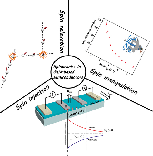
Graphical Abstract
1 Introduction
Nowadays, conventional complementary metal oxide semiconductor (CMOS) devices encounter a performance bottleneck as the feature size approaches the physical limit. The International Technology Roadmap of Semiconductors (ITRS) has identified several alternate technologies that have the potential to optimize current CMOS technology. Spintronics, which focuses on manipulating electron spin degrees of freedom, is one of the feasible routes to continue the miniaturization of integrated circuits due to its potentials of high integration, low power consumption, and high operating speed [Citation1–4].
Metal-based spintronic devices have been widely used in logic memory applications for the discovery of giant magnetoresistance. Compared with metals, semiconductors have also received extensive attentions in spintronics over the past decades. The semiconductor spintronic devices mainly include spin-LEDs [Citation5], spin-lasers [Citation6], spin field effect transistors (SFETs) [Citation7] and magnetic bipolar transistors [Citation8], etc. The core of these semiconductor spintronic devices is to convert the intrinsic spin information into electrical and optical output signals. Hence, efficient spin injection, suppressed spin relaxation, and artificial spin manipulation are issues worthy of attention in semiconductor spintronic device development.
The premise of spintronic device operation is to polarize the carriers spin in the semiconductors. Generally, spin injection methods contain optical injection and electrical injection [Citation9,Citation10]. Optical spin injection is a simple and efficient method, but the optical spin injection is not conducive to the device integration. Electrical spin injection is beneficial to integrate with current technology, and it is generally assisted by ferromagnetic metals. However, there is a conductance mismatch between the ferromagnetic metals and the semiconductors, which results in low efficiency of spin injection [Citation11–13]. Spin injection tunneling barriers, such as MgO (Al2O3) [Citation14–18] or Schottky barriers [Citation19–21] are widely employed to address this problem and improve spin-injection polarization. However, the spin tunneling injection would be greatly aggravated by interface localized states [Citation22–25], the interface random magnetic field [Citation26,Citation27] and the interface energy band bending [Citation28,Citation29]. Therefore, an excellent tunneling junction is necessary to realize the efficient electrical spin injection. It is worth noting that the Curie temperature of GaN-based diluted magnetic semiconductors was expected to be higher than room temperature [Citation30–32], which could solve the conductance mismatch problems diametrically.
After injecting spin-polarized carriers into the non-magnetic semiconductor, the non-equilibrium spin-polarized carriers will relax to an equilibrium state, thus affecting the operation of spintronic devices. The spin relaxation mechanisms in semiconductors mainly involve Elliott-Yafet (EY) mechanism, D’yakonov-Perel’ (DP) mechanism, Bir-Aronov-Pikus (BAP) mechanism, and nuclear spin hyperfine interaction effect [Citation33–36]. For GaN-based semiconductors, the spin relaxation of conduction band electrons is mainly determined by the DP relaxation mechanism [Citation37–39]. Since bulk GaN has the weak inherent spin-orbit coupling [Citation40], the DP spin relaxation will be weakened [Citation41,Citation42], and thus the spin polarization can survive a long time within spintronic devices.
In order to satisfy the demands of integrated circuit logic operations, a controllable output signal should be realized in spintronic devices. The spin-orbit coupling plays a decisive role in the artificial manipulation of spins because it can be modulated by gate voltage [Citation43], interface effect [Citation44] and even the crystal orientation of semiconductor channel [Citation45]. The gate-controlled spin-orbit coupling can adjust the spin precession rate as discussed in the SFET concept [Citation4,Citation46–48]. The spin relaxation rate [Citation49] and spin diffusion length [Citation50] can be regulated by gate-controlled spin-orbit coupling as well. For the GaN-based heterostructures, the controllable manipulation of the spin-orbit coupling can be directly realized by modulating the piezoelectric polarization field under uniaxial strain [Citation51–53].
In this review, we present the fundamental conception of spin-orbit coupling in GaN-based semiconductors in Section 2. After a brief introduction of the DP spin relaxation mechanism, the spin relaxation dynamics of GaN-based semiconductors measured by circularly polarized spectroscopy are described in Section 3. We focus on the electrical spin injection with magnetotransport measurements in Section 4 and the influences of polarization field in GaN-based heterostructures on spin manipulation in Section 5. Finally, the status quo and outlook of spintronic devices are presented in Section 6 and a conclusion is presented in Section 7.
2 Spin-orbit coupling in GaN-based semiconductors
Spin-orbit coupling plays a key role in semiconductor spintronics research. It can induce spin relaxation and realize spin manipulation. According to the special theory of relativity, an electron moving in an electric field is affected by an effective magnetic field. This interaction between the electron spin and the effective magnetic field induces spin-orbit coupling. The corresponding spin-orbit coupling Hamiltonian is
where m0 is the electron mass, is the reduced Planck constant, c is the speed of light,
is the Pauli matrix of the electron, V is the electric potential, and
is the canonical momentum. In semiconductors, the motion of electrons can be described by the Bloch wave vector
. The potential V includes the periodic potential of the lattice and the applied potential. Since the periodic potential of a semiconductor lattice is closely related to its crystal structure, the spin-orbit coupling basically depends on the symmetry of the semiconductor.
When semiconductor satisfies the space inversion and the time reversal symmetry simultaneously, its energy band has spin degeneracy [Citation36]. Thus, the emergency of spin-orbit coupling Hamiltonian requires breaking one of these two symmetries. The time reversal symmetry is usually broken by means of an external magnetic field. The breaking of the spatial inversion symmetry comes from the bulk inversion asymmetry (BIA) of the constituent material itself or the structural inversion asymmetry (SIA) introduced by the extrinsic electric field.
GaN belongs to the hexagonal wurtzite structure without spatial inversion symmetry. Owing to the BIA, GaN electrons have non-zero spin-orbit coupling Hamiltonian which can be expressed as . The effective magnetic field is in the form of [Citation37]
where kx, ky, kz are the wave vectors in the directions of x, y, z (,
,
),
,
is the Rashba term coefficient and
and b are the parameters of Dresselhaus spin-orbit coupling term [Citation37]. The Rashba term coefficient
(
from weak antilocalization experiments by other group) and the Dresselhaus term parameters
and b = 3.959 (a dimensionless constant characterizing anisotropy) [Citation54–56]. Unlike the case of zinc blende semiconductors, the k-linear Rashba term appears in the intrinsic spin-orbit coupling Hamiltonian of GaN due to hexagonal wurtzite characteristics [Citation57,Citation58].
In addition to the spin-orbit coupling generated by the periodic lattice potential of the crystal, the applied electric field generated by the gate voltage or the built-in electric field in the heterostructures can also generate Rashba spin-orbit coupling due to the SIA. With the Löwdin partition method, this Rashba spin-orbit coupling Hamiltonian can be simply written as [Citation36]
here is the Rashba spin-orbit coupling coefficient, which is proportional to the strength of the extrinsic electric field [Citation43,Citation59], and
is the unit vector along the direction of the electric field. In GaN-based heterostructures or top-gate devices, the external electric field is usually parallel to the c-axis (z direction,
), and the resulting Rashba spin-orbit coupling has the same form as the k-linear term in BIA spin-orbit coupling of GaN, which is,
.
In GaN-based heterostructures or quantum wells, the spin-orbit coupling is small as compared to the Fermi energy of the system, and thus the Fermi contours are almost circles [Citation60]. In one band occupied case, in EquationEquation 2
(2) can be replaced by the square of the Fermi wave vector
, where
is the electron sheet density [Citation60]. Therefore, the effective magnetic field can be expressed as [Citation60]
Considering the quantum confinement in heterojunctions, the term becomes a parameter depending on the well width, which can be designed to enhance spin relaxation time [Citation51]. Further, in the AlGaN/GaN heterostructures, the total spin-orbit coupling coefficient can attain
[Citation61]. The researchers confirmed that Rashba coefficient was about ten times larger than Dresselhaus coefficient by using the circular photogalvanic effect (CPGE) in AlGaN/GaN heterostructures indicating that Rashba effect was the dominant factor [Citation53]. The large Rashba spin-orbit coupling is proven to be relevant to the strong spontaneous and piezoelectric polarization at the heterointerface in GaN-based heterostructures [Citation52,Citation53,Citation61]. The built-in polarization electric field has been modulated by methods such as adjustments of the barrier layer Al compositions [Citation61], illuminations [Citation62] and uniaxial strains [Citation52,Citation53] in AlGaN/GaN heterostructures.
For quasi-one-dimensional GaN nanowires (NWs), its intrinsic spin-orbit coupling form is the same as the bulk GaN. However, due to the high surface-to-volume ratio, the SIA induced by the surface electric field introduces an extrinsic effective magnetic field. This corresponding effective magnetic field of a wurtzite GaN NW with the growth direction along [0001] can be expressed as
where and
are the spin-orbit coupling coefficients governing the strength of the surface-induced effective magnetic field perpendicular and parallel to the wurtzite GaN NWs c-axis. As shown in [Citation63], the intrinsic effective magnetic field and surface-induced effective magnetic field have different distribution planes in momentum space, which are perpendicular to each other. It is worth noting that the surface-induced effective magnetic field can greatly affect spin relaxation [Citation64] and thus needs to be carefully considered.
Figure 1. (a) The distribution of the intrinsic spin-orbit coupling effective magnetic field in momentum space. (b) The interface spin-orbit coupling effective magnetic field in momentum space [Citation63].
![Figure 1. (a) The distribution of the intrinsic spin-orbit coupling effective magnetic field in momentum space. (b) The interface spin-orbit coupling effective magnetic field in momentum space [Citation63].](/cms/asset/dd9391d0-51eb-4da2-9a00-56e923a9a056/tapx_a_2158757_f0001_oc.jpg)
3 Spin relaxation dynamics in GaN-based semiconductors
Spin relaxation refers to the process in which a carrier ensemble with spin polarization evolves with time, and the spin polarization gradually disappears. Preservation of spin information is important for spintronic device operation, and both Dresselhaus spin-orbit coupling and Rashba spin-orbit coupling will lead to spin relaxation.
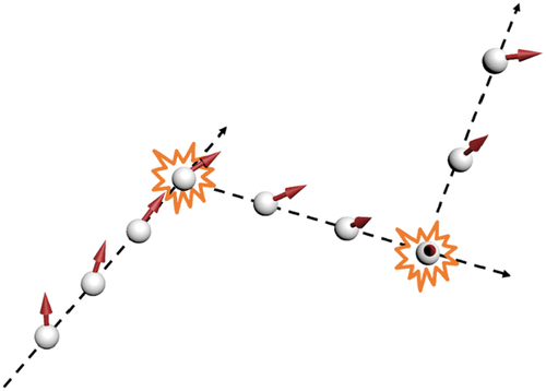
The behavior of spin relaxation of GaN conduction band electrons is explained by the DP spin relaxation mechanism [Citation37–39]. The physical image of the DP spin relaxation mechanism is briefly introduced as follows. The spin-orbit coupling is related with momentum , as shown in EquationEquation 1
(1) , meaning that the effective field
depends on
(EquationEquation 2
(2) ). The direction and magnitude of
varies with the change of
due to the scattering, and thus leads to a change in spin precession angle as shown in . Meanwhile, the faster the momentum relaxation, the slower the spin dephasing since the electron barely has enough time to cause a spin flip by precession, i.e. spin relaxation time is inversely proportional to momentum scattering time. The theoretical formula of DP spin relaxation rate is expressed as
Figure 2. Illustration of the DP spin relaxation mechanism. The spin precesses around a randomly fluctuating magnetic field caused by scattering events and thus loses its initial polarization message.
where is the momentum scattering time,
denotes averaging over the momentum distribution of electrons,
is the spin-orbit coupling induced effective magnetic field and
. It can be seen that the spin relaxation time
is inversely proportional to
.
In 2010, J. H. Buss et al. presented an analytic expression based on DP mechanism to describe the spin relaxation in bulk GaN [Citation37]. Assuming a Boltzmann distribution for the electron momentum, an isotropic effective electron mass m* = 0.2 m0 and neglecting the dependence of b, the DP relaxation rate of bulk GaN electron spins can be evaluated as [Citation37]
where ,
,
are the spin relaxation rate for Rashba contribution, Dresselhaus contribution, and interference term, T is the temperature, and kB is the Boltzmann constant. Here, we assume that the spin polarization is along the z-axis of GaN. As demonstrated in previous works [Citation54,Citation56],
and
. For a momentum scattering time
, the temperature-dependent spin relaxation times are calculated by EquationEquation 7
(7) as shown in . It is obvious that the spin relaxation in bulk GaN is almost completely governed by the Rashba term contribution.
Figure 3. (a) Temperature dependence of the calculated spin relaxation time for only the Rashba contribution (dotted red line), for only the Dresselhaus contribution (dashed blue line) and for both contributions including the interference term (solid black line), for a scattering time
= 40 fs. (b) Temperature dependence of the spin relaxation time
in the absence of an applied magnetic field (black triangles) and in the presence of an applied magnetic field (red circles), respectively. The line shows spin relaxation time calculated according to EquationEquation 7
(7) for a scattering time
= 40 fs [Citation37].
![Figure 3. (a) Temperature dependence of the calculated spin relaxation time for only the Rashba contribution (dotted red line), for only the Dresselhaus contribution (dashed blue line) and for both contributions including the interference term (solid black line), for a scattering time = 40 fs. (b) Temperature dependence of the spin relaxation time in the absence of an applied magnetic field (black triangles) and in the presence of an applied magnetic field (red circles), respectively. The line shows spin relaxation time calculated according to EquationEquation 7(7) for a scattering time = 40 fs [Citation37].](/cms/asset/680ac553-e88b-4929-9ae4-c792e6c0b5cc/tapx_a_2158757_f0003_oc.jpg)
Furthermore, the researchers used time resolved Kerr rotation (TRKR) experiment to verify the above theoretical analysis [Citation37]. TRKR measurement is a pump-probe circularly polarized spectroscopy, which can detect the spin relaxation process with ultrahigh time resolution and give the spin relaxation time directly. As shown in , the spin relaxation time measured by TRKR experiments fits well with the time calculated theoretically by EquationEquation 7(7) . At the same time, the external magnetic field increases the spin relaxation time by a factor of 4/3 as depicted in . This increasing relaxation time with the magnetic field originates from the anisotropy of the effective magnetic field [Citation38,Citation41].
The effects of doping concentration [Citation65] on spin relaxation of bulk GaN have also been thoroughly studied. The shallow bound states introduced by doping donor impurities such as Si in GaN can yield a longer spin relaxation time. The longest spin relaxation time of the conduction band electrons occurs at the carrier density nc which is determined via and usually locates near the metal-semiconductor phase transition point at room temperature (the doping concentration of the GaN sample is about
[Citation66]). The non-monotonic decrease of spin relaxation time with doping concentration is verified in heavily doped degenerate GaN, and the obtained dependence
in the degenerate regime is consistent with the DP mechanism [Citation67].
Recently, the effect of GaN fine band structure on spin relaxation dynamics was revealed by S. X. Zhang et al. [Citation9]. Three reversals of the spin orientation and a remarkable reduction of spin relaxation time were found in experiments, which was caused by the photon-energy dependent transitions from the heavy and light hole bands to the exciton levels and the conduction band edge. It is worth noting that most of the GaN spintronic device researches are based on conduction band electrons because GaN holes have short spin lifetime caused by the valence band mixing [Citation68].
At the GaN-based heterojunction interface, the two-dimensional electron gas (2DEG) induced by a strong polarization field has ultra-high mobility and high concentration, which is very suitable for electronic devices. Therefore, it is very necessary to study the spin relaxation properties of 2DEG.
Lately, S. X. Zhang et al. investigated the spin dynamics in GaN/Al0.1Ga0.9N quantum well with complex band edge structure by photon-energy dependent TRKR experiment [Citation69]. The electron spin relaxation time of 7 ps in the quantum well is much shorter than that of 40 ps in the bulk GaN or 140 ps in Al0.1Ga0.9N barrier layer due to the built-in polarization electric field [Citation69] as depicted in . According to the Boltzmann distribution of the electron momentum at room temperature, the DP spin relaxation time can be expressed as [Citation69]
Figure 4. (a) TRKR signals at an excitation energy of 3.402 and 3.573 eV, corresponding to the electron spin relaxation in the bulk GaN buffer layer and the Al0.1Ga0.9N barrier. (b) TRKR signals at an excitation energy of 3.513 eV, corresponding to the spin relaxation of two-dimensional electron gas in the GaN quantum well [Citation69].
![Figure 4. (a) TRKR signals at an excitation energy of 3.402 and 3.573 eV, corresponding to the electron spin relaxation in the bulk GaN buffer layer and the Al0.1Ga0.9N barrier. (b) TRKR signals at an excitation energy of 3.513 eV, corresponding to the spin relaxation of two-dimensional electron gas in the GaN quantum well [Citation69].](/cms/asset/23149084-117e-4257-a14d-95deed920ee7/tapx_a_2158757_f0004_oc.jpg)
which indicates that the larger spin-orbit coupling can cause shorter spin relaxation time. The shorter spin relaxation time of the quantum well measured in the experiments is consistent with EquationEquation 8(8) , demonstrating the built-in electric field can greatly affect the electron spin dynamics [Citation69]. Subsequently, this research group continued to study the spin relaxation dynamics of 2DEG at the AlGaN/GaN heterojunction interface. Combined with the variable temperature TRKR experiment and Hall measurement, at the AlGaN/GaN interface, 2DEG has spin diffusion length up to 313 nm due to its high electron mobility. Even at room temperature, the spin diffusion length of 2DEG can reach 174 nm as well [Citation70].
According to EquationEquation 6(6) , the spin relaxation time under the DP mechanism is inversely proportional to the variance of the spin-orbit coupling effective magnetic field. In the case of one-dimensional NWs with radial quantum confinement, the orientation of the electron Bloch wave vector is restricted to a certain direction, resulting in a reduction in the spin-orbit coupling effective magnetic field variance determined by the momentum distribution.
It has been theoretically concluded that the spin relaxation in GaN NWs with mesoscopic confinement is found to be governed by the cubic Dresselhaus term, which is almost negligible for spin relaxation in the bulk [Citation71]. As investigated by J. H. Buß, the spin relaxation rate of GaN NWs at temperatures above 100 K could be well fitted by the DP mechanism, but it was much higher than the theoretical value when k-cubic spin-orbit coupling term dominated [Citation64]. The reason for that is the existence of the surface-induced effective magnetic field as expressed in Section 2. Previous studies have shown that the surface electric field of GaN NWs originates from surface localized states [Citation72,Citation73]. Recently, X. C. Liu et al. used CPGE to demonstrate that the Fermi level pinning of the surface states resulted in a weak modulation of the surface-field-induced spin-orbit coupling by gate voltage [Citation63]. Since the spin manipulation demands effective regulation of spin-orbit coupling, the realization of GaN NW-based spintronic devices needs suppression of the interfacial spin-orbit coupling, which requires in-depth analysis of the surface states in GaN NWs in subsequent studies [Citation74,Citation75].
4 Electrical Spin injection in GaN-based semiconductors
The efficient spin injection into semiconductors is a critical issue in semiconductor spintronics. As mentioned in the above discussion, spin injection methods contain optical spin injection and electrical spin injection. Optical spin injection is a process that uses circularly polarized light to excite spin-polarized carriers in semiconductors and is closely related to the optical selection rule for the fine band structure of semiconductors. In wurtzite GaN, the valence band splits into heavy-hole band (HH band, Γ9 symmetry), light-hole band (LH band, Γ7 symmetry), and crystal-field split-off band (CH band, Γ7 symmetry). It is noteworthy that the HH and LH bands of wurtzite GaN have obvious energy splitting. Considering the optical selection rule of the transition from HH and LH bands to conduction band, the spin polarization of the photogenerated carriers can reach up to 100% when the energy of circular polarized light resonates with various fine energy levels. This light-helicity controllable spin orientation can be utilized for optical information storage [Citation76] but is not conducive to the device integration of modern circuits. Up to now, the optical spin injection into GaN-based semiconductors has been mainly used to explore the properties of spin dynamics, for example TRKR spectroscopy [Citation9,Citation37,Citation64,Citation69,Citation70], CPGE [Citation52,Citation53,Citation63], anomalous CPGE [Citation77], and photoinduced anomalous Hall effect [Citation78] etc.
As discussed above, the electric spin injection is affected by the conductance mismatch problem. A spin injection tunneling barrier or a diluted magnetic semiconductor has been proven effective to solve this problem [Citation36].
The conductivity of diluted magnetic semiconductor is an order of magnitude of the non-magnetic semiconductor channel and the diluted magnetic semiconductor can be epitaxially grown in situ as well. As a result, it is possible to achieve high spin injection efficiency by using diluted magnetic semiconductors as spin polarization sources. As a representative diluted magnetic semiconductor, (Ga, Mn)As has realized spin injection into GaAs-based semiconductors at low temperature [Citation79,Citation80]. The Curie temperature of (Ga, Mn)As is about 173 K [Citation81] that hinders the development of room temperature devices. As shown in , GaN was predicted to have a higher Curie temperature compared with other materials [Citation82] and a Curie temperature as high as 940 K was reported for GaN in 2002 [Citation83]. GaN-based diluted magnetic semiconductors have been used to be the spin injectors for the spin-LEDs [Citation84,Citation85]. D. Banerjee et al. used Cr-doped GaN to realize the electrical spin injection into GaN-based quantum wells. The circular polarization degree of luminescence of the spin-LEDs based on this injector is 2.5% at 200 K [Citation84]. The room temperature spin injection has been achieved through Mn-doped GaN [Citation85]. However, the saturation magnetization of GaN-based diluted magnetic semiconductors is still small and the spin-injection polarization is to be improved.
Figure 5. Computed values of the Curie temperature TC for variable semiconductors. P-type Mn-doped GaN can attain a TC above room temperature [Citation82].
![Figure 5. Computed values of the Curie temperature TC for variable semiconductors. P-type Mn-doped GaN can attain a TC above room temperature [Citation82].](/cms/asset/e9f22c54-a3a6-4c97-a26d-e48ff79e6d63/tapx_a_2158757_f0005_oc.jpg)
Another technical route to achieve electrical spin injection is the fabrication of spin tunneling junctions. However, the injection process is greatly affected by the quality of the tunneling junction [Citation22–25]. In order to determine the effective spin injection and quantitatively obtain the tunneling junction quality, the Hanle effect [Citation86] and the non-local magnetoresistance [Citation87] of lateral non-local spin valve in GaN-based semiconductors have been studied in the past few years.
As depicted in , the four-terminal spin valve is a non-local geometry, which can be divided into a spin injection loop (Electrodes I and II) and a spin detection loop (Electrodes III and IV). Electrodes II and III with different coercivities are spin injection junction and spin detection junction, which can be magnetized either in parallel or antiparallel directions. Electrodes I and IV are positioned far away from the middle two electrodes, which ensures that the average spin polarization at Electrodes I and IV is essentially zero [Citation88]. A constant current Iinject passes through Electrodes I and II, and then a spin dependent voltage Vs [Citation89] is generated between Electrodes III and IV due to the difference in the spin dependent electrochemical potential of the diffusing electrons.
Figure 6. Illustration of the non-local four terminal spin valve. In this geometry, spin-polarized carriers diffuse from injection Electrode II to detection Electrode III. The spin polarization will generate a spin dependent voltage between Electrode III and distal Electrode IV. Hanle effect signal and non-local magnetoresistance signal can be obtained by the magnetotransport measurement under different magnetic field angles.
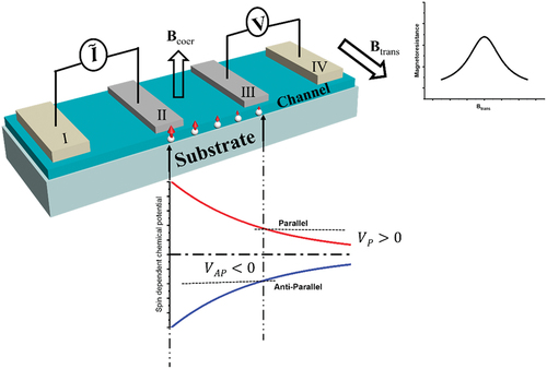
With the magnetic field Bcoer sweeping, the spin dependent voltage will be positive (negative) by manipulating the spin injection Electrode II and the detection Electrode III to be parallel (antiparallel) magnetization, then giving a measurement of the non-local magnetoresistance. The channel length L dependent non-local magnetoresistance can be investigated to estimate the spin-injection polarization Pinject and spin diffusion length using the equation
where is the non-local magnetoresistance,
is the measured non-local voltage equals to 2
,
is the resistivity of the semiconductor, and A is the cross-sectional area of the semiconductor. Pinject and
can be obtained by fitting the
experimental curve with a linear function.
Meanwhile, the Hanle effect signal will appear when the transverse magnetic field Btrans is applied. This signal originates from the spin precession as well as spin dephasing of the diffusing electron spins. The spin relaxation time can be obtained by fitting the Hanle effect expression which is
where Ds is the spin diffusion coefficient and is the Larmor precession frequency, which is proportional to Btrans. The (+) and (-) sign corresponds to the parallel and antiparallel magnetization of Electrodes II and III, respectively. It can be seen that the Hanle effect and the non-local magnetoresistance are essential to judge the electrical spin injection into semiconductors and extract the spin transport parameters.
In 2012, researchers grew a MnAs (ferromagnetic layer, 35 nm)/AlAs (tunneling layer, 1 nm) injection junction on bulk GaN by molecular beam epitaxy (MBE) [Citation90]. This tunneling junction effectively suppresses the interface state density through MBE growth, and thus achieves a high-quality injection structure. A three-terminal spin valve (Electrodes II and III are the same electrode) has successfully realized room temperature spin injection. The spin relaxation time is 44 ps extracted from the three-terminal Hanle signals which are expressed as
by simplifying EquationEquation 10(10) . And the spin diffusion length reaches 175 nm calculated through the relation
. It is worth noting that the three-terminal spin valve measurement replaces the spin diffusion coefficient Ds with the charge diffusion coefficient De, so the spin diffusion length cannot be accurately extracted. Four years later, A. Bhattacharya et al. successfully fabricated a GaN four-terminal non-local spin valve by electron beam evaporation of FeCo(80 nm)/MgO(1 nm) as a spin injection junction [Citation91]. The non-local magnetoresistance of four-terminal spin valve is shown in [Citation91]. According to the channel length-dependent magnetoresistance, the spin-injection polarization and spin diffusion length are 7.9% and 137 nm, respectively. A spin relaxation time of 37 ps is obtained from the four-terminal Hanle effect signals as depicted in [Citation91]. From the relationship
, the spin diffusion length is estimated to be 176 nm, which is consistent with the value derived from the non-local magnetoresistance measurements within the limits of errors [Citation91].
Figure 7. (a) Non-local magnetoresistance as a function of applied magnetic field in GaN-based four-terminal spin valve (channel length is 250 nm) at room temperature. The black and red lines indicate increasing and decreasing magnetic field sweeps, respectively. (b) Hanle effect signal measured for a four-terminal spin valve at 300 K. The red and green lines correspond to parallel and antiparallel magnetization of the two ferromagnetic electrodes. The spin relaxation time is 37 ps by fitting the experimental curve and the spin diffusion length is about 176 nm by using [Citation91].
![Figure 7. (a) Non-local magnetoresistance as a function of applied magnetic field in GaN-based four-terminal spin valve (channel length is 250 nm) at room temperature. The black and red lines indicate increasing and decreasing magnetic field sweeps, respectively. (b) Hanle effect signal measured for a four-terminal spin valve at 300 K. The red and green lines correspond to parallel and antiparallel magnetization of the two ferromagnetic electrodes. The spin relaxation time is 37 ps by fitting the experimental curve and the spin diffusion length is about 176 nm by using [Citation91].](/cms/asset/12f20149-d73c-40a8-a562-ff7d99e5f925/tapx_a_2158757_f0007_oc.jpg)
Recently, X. C. Liu et al. systematically studied the influences of interfacial effects on GaN spin injection junctions by three-terminal spin valve measurements [Citation92]. The spin scattering induced by surface random magnetic fields at low temperatures was observed. This additional spin relaxation process has been confirmed by the inverted Hanle effect, which is commonly recognized as a spin-dependent signal caused by rough interface [Citation24], as shown by the black line in . Compared with sample A, the root-mean-square roughness (RMS) of sample B is lower, that is, it has a smoother surface, which suppresses the spin relaxation induced by the random magnetic field and the inverted Hanle effect disappears. Furthermore, the spin relaxation process induced by surface band bending can be effectively suppressed with increasing temperature and the large injection current can also reduce the probability of spin-polarized electrons being trapped by surface localized states. These conclusions are confirmed by comparison with the intrinsic spin relaxation time measured by TRKR spectroscopy as illustrated in .
Figure 8. (a) The Hanle (red line) and inverted Hanle (black line) curves in sample A at 2 K. (b) The Hanle curve (red line) and vanished inverted Hanle curve (black line) in sample B at 9 K. (c) extracted by Hanle curves (green symbols) under Iinj = 0.1 mA and TRKR measurements (black box symbols) in sample B at various temperatures. The corresponding bias voltage is also shown as red symbols. (d) The bias current-dependent
and bias voltage at 160 K. The corresponding
extracted from TRKR is also shown [Citation92].
![Figure 8. (a) The Hanle (red line) and inverted Hanle (black line) curves in sample A at 2 K. (b) The Hanle curve (red line) and vanished inverted Hanle curve (black line) in sample B at 9 K. (c) extracted by Hanle curves (green symbols) under Iinj = 0.1 mA and TRKR measurements (black box symbols) in sample B at various temperatures. The corresponding bias voltage is also shown as red symbols. (d) The bias current-dependent and bias voltage at 160 K. The corresponding extracted from TRKR is also shown [Citation92].](/cms/asset/fcb9655e-6021-4265-8868-5bc29461dc52/tapx_a_2158757_f0008_oc.jpg)
With the gradual maturity of the spin tunneling junction fabrications in GaN-based semiconductors, a spin-injection polarization of 12% has been realized by magnetron sputtering and atomic layer deposition of Co/Al2O3 at room temperature based on bulk GaN [Citation93]. By integrating this optimized spin tunneling junction into GaN-based spin-LEDs, a circular polarization of 9.2% was achieved at room temperature [Citation93].
It is worth noting that it is not easy to realize spin injection in GaN-based heterostructures. There is a large conductance mismatch between the ferromagnet and the barrier of the 2DEG, and the extra spin dephasing in the barrier is also the obstacle. The effective spin injection requires the thickness of the barrier layer to be very thin. However, the 2DEG of general AlGaN/GaN will be greatly affected or even disappear when the barrier layer is less than 5 nm [Citation94,Citation95]. AlN/GaN heterostructures [Citation96] and In0.18Al0.82N/GaN heterostructures[Citation97] have been proven to have ultra-thin barrier layers in previous studies, respectively. In 2021, X. Y. Zhang et al. achieved the first efficient electric spin injection into GaN-based 2DEG by using AlN/GaN heterostructures [Citation98]. The innovative idea in the experiment is that the 2.5 nm AlN barrier layer was used as the barrier layer of the heterostructure as well as the tunneling layer to overcome conductance mismatch simultaneously, as shown in [Citation98]. As shown in , the coexistence of the Hanle and inverted Hanle effect signals in the same device guarantees the validity of spin injection.
Figure 9. (a) Illustration of electron spin injection with Co/AlN/GaN structure. Ef refers to Fermi level. E1 and E2 are schematic wave functions of the two sub-bands existing in the AlN/GaN heterostructure. (b) Three-terminal magnetoresistance under a magnetic field perpendicular and parallel to the surface at 55 K with AC 0.3 mA. Inset shows zero-bias resistance as a function of temperature of one junction [Citation98].
![Figure 9. (a) Illustration of electron spin injection with Co/AlN/GaN structure. Ef refers to Fermi level. E1 and E2 are schematic wave functions of the two sub-bands existing in the AlN/GaN heterostructure. (b) Three-terminal magnetoresistance under a magnetic field perpendicular and parallel to the surface at 55 K with AC 0.3 mA. Inset shows zero-bias resistance as a function of temperature of one junction [Citation98].](/cms/asset/90b56ef4-2786-4895-b4e1-1c8c89c25d8f/tapx_a_2158757_f0009_oc.jpg)
In 2012, researchers at the University of Michigan fabricated a MgO/CoFe (1 nm/60 nm) spin tunneling junction based on a single GaN NW [Citation99]. A scanning electron microscope image of this device is shown in . From the magnetoresistance and spin accumulation measurements, the spin diffusion length and spin relaxation time of the NW spin valve are 260 nm and 100 ps at room temperature, respectively, which are much higher than those of the bulk GaN. The downside of this device is the spin-injection polarization of only 0.7%. Five years later, the spin-injection polarization of four-terminal non-local spin valve based on GaN NWs grown perpendicular to the non-polar plane was confirmed to achieve 9% at room temperature, while the spin diffusion length and spin relaxation time also reached 710 nm and 150 ps, respectively [Citation100]. These single-crystal NWs have a triangular cross-section defined by the ,
and
planes to explore the crystallographic dependence of spin transport as shown in . Researchers found that the spin injection and the spin transport were closely related to the spontaneous polarization in polar face or semi-polar face of these trigonal GaN NWs [Citation100].
Figure 10. (a) A SEM figure of the lateral spin valve fabricated on a 4 long NW using e-beam lithography. Electrodes 1 and 4 are non-ferromagnetic Ti/Au detector contacts and Electrodes 2 and 3 are the ferromagnetic tunnel contacts [Citation99]. (b) Schematic cross-sectional view of ferromagnetic electrode in contact with the GaN NW and the high-angle annular dark field images with the 40 nm scale bars [Citation100].
![Figure 10. (a) A SEM figure of the lateral spin valve fabricated on a 4 long NW using e-beam lithography. Electrodes 1 and 4 are non-ferromagnetic Ti/Au detector contacts and Electrodes 2 and 3 are the ferromagnetic tunnel contacts [Citation99]. (b) Schematic cross-sectional view of ferromagnetic electrode in contact with the GaN NW and the high-angle annular dark field images with the 40 nm scale bars [Citation100].](/cms/asset/bc7aefcb-7f96-4a1e-ab09-d95a637f1d43/tapx_a_2158757_f0010_oc.jpg)
From bulk GaN to GaN-based low-dimensional structures, spin injection has been successfully implemented and gradually optimized to improve efficiency. These research results lay the foundation for the subsequent development of GaN-based spintronic devices.
5 Spin manipulation in GaN-based heterostructures
An important manner for spin manipulation is to control the spin-orbit coupling interaction. The Rashba spin-orbit coupling has been proven to play an indispensable role in the GaN-based semiconductors, especially GaN-based heterostructures due to the polarization field [Citation51–53,Citation61,Citation69]. Therefore, in order to realize the spin manipulation of GaN-based heterostructures, the artificial control of the polarization electric field is an important research topic.
In 2007, N. Tang et al. investigated the spin-orbit coupling strength via various Al compositions in AlGaN/GaN heterostructures [Citation61]. It is found that the spin-orbit coupling coefficient in the AlGaN/GaN heterostructures increases with the increasing piezoelectric polarization electric field, which depends on the Al composition of the barrier layer. This research group also adjusted the spin splitting of 2DEG in the AlGaN/GaN heterostructures by illumination as shown in [Citation62]. The illumination increases the concentration of 2DEG to enhance the screening effect of the built-in electric field at the heterointerface, thereby reducing the Rashba spin-orbit coupling. However, the composition changes of the barrier layer or the influences of illumination make it difficult to quantitatively control the spin-orbit coupling in the GaN-based heterostructures.
Figure 11. The second derivative of the Shubnikov–de Haas (SdH) oscillation resistance of the 2DEG in AlGaN/GaN heterostructure (a) before and (b) after the illumination as a function of the applying magnetic field. After the illumination, the beating nodes shift to lower magnetic field which indicates the decrease of the zero-field spin-splitting energy [Citation62]. (c) The amplitude of the CPGE current (proportional to the spin-orbit coupling strength) as a function of the uniaxial strain in Al0.30Ga0.70N/GaN heterostructure. The current increases linearly with increasing uniaxial strain and the inset shows the schematic diagram of the uniaxial strain equipment [Citation53].
![Figure 11. The second derivative of the Shubnikov–de Haas (SdH) oscillation resistance of the 2DEG in AlGaN/GaN heterostructure (a) before and (b) after the illumination as a function of the applying magnetic field. After the illumination, the beating nodes shift to lower magnetic field which indicates the decrease of the zero-field spin-splitting energy [Citation62]. (c) The amplitude of the CPGE current (proportional to the spin-orbit coupling strength) as a function of the uniaxial strain in Al0.30Ga0.70N/GaN heterostructure. The current increases linearly with increasing uniaxial strain and the inset shows the schematic diagram of the uniaxial strain equipment [Citation53].](/cms/asset/c0acbb81-e30d-451e-84f7-1612368cf077/tapx_a_2158757_f0011_b.gif)
The strong piezoelectric polarization field in AlGaN/GaN heterostructures mainly originates from the large tensile strain in the AlGaN barrier layer [Citation101]. Therefore, applying an external strain can effectively and quantitatively control the built-in electric field strength [Citation51–53].
The spin-orbit coupling strength in the Al0.25Ga0.75N/GaN heterostructure was investigated and found to be sensitive to the applied uniaxial strain through CPGE measurements [Citation52]. The CPGE amplitude, which is proportional to the spin-orbit coupling coefficient, increased linearly with increasing uniaxial strain on the heterostructures [Citation52]. Also, using uniaxial strain to change piezoelectric polarization, C. M. Yin et al. systematically performed CPGE measurements on AlGaN/GaN heterostructures with different Al composition barrier layers [Citation53]. They found that the spin-orbit coupling strength could be effectively manipulated by uniaxial strain regardless of the composition of the barrier layers as illustrated in ) [Citation53]. Extracted from the relationships between the spin-orbit coupling and the uniaxial strain, the ratio of the Rashba spin-orbit coupling coefficient to the Dresselhaus spin-orbit coupling coefficient is around 10, indicating the Rashba effect dominates in AlGaN/GaN heterostructures [Citation53].
What is amazing is that in InGaN/GaN quantum wells has opposite sign with
[Citation102,Citation103], which is different from AlGaN/GaN heterostructures because of the different interface-strain-induced piezoelectric polarization. X. C. Liu et al. used InGaN/GaN quantum wells to realize the mutual cancellation of Rashba and Dresselhaus spin-orbit couplings and to achieve effective manipulation of spin relaxation through uniaxial strain [Citation51].
In InGaN/GaN quantum wells, because of the quantum confinement along c-direction and low doping level in the system, i.e. , the k-cubic Dresselhaus term spin-orbit coupling associated with
can be ignored [Citation51]. The large
term (InGaN potential well width d = 3.5 nm and
) leads to the fact that the Dresselhaus term on spin relaxation should be considered [Citation51]. Taking the Rashba term and the Dresselhaus term and their interference term into account in the DP spin relaxation mechanism, the spin relaxation time can be written as [Citation51]
The ratio in InGaN/GaN quantum wells can approach −1, thus resulting in a long spin lifetime as shown in . The spin relaxation time of the 2DEG in the designed InGaN/GaN quantum well is as long as 311 ps at room temperature, which is an order of magnitude higher than that of the electron spin relaxation time in bulk GaN. In addition, the researchers successfully controlled the piezoelectric polarization electric field in the quantum well with uniaxial strain, resulting in a significant change in the spin relaxation time as depicted in . The extracted ratios
vary as a function of the external strain and polarization electric field is shown in . This linear fitting curve not only proves the effective manipulation of spin-orbit coupling through uniaxial strain but also indicates that the external tensile strain can only weaken the initial piezoelectric polarization, thus increasing the ratio from −0.81 to −0.61. With the ratio
, the extremely long spin relaxation time will surely benefit the spin transport process and greatly enhance the performance of relevant spintronic devices [Citation51]. Therefore, higher initial piezoelectric polarization field (i.e. higher In composition) and narrower well width are needed to achieve this ideal ratio [Citation51].
Figure 12. (a) The TRKR results of InGaN/GaN multi quantum wells and bulk GaN without external strain. (b) The TRKR signals of InGaN/GaN multi quantum wells under external strains. (c) The extracted Ʈs of InGaN/GaN multi quantum wells under various strains. Insets show the equipment used to apply external uniaxial strain. (d) The extracted ratios vary as a function of the external strain and polarization electric field, and the red line shows the linear fitting [Citation51].
![Figure 12. (a) The TRKR results of InGaN/GaN multi quantum wells and bulk GaN without external strain. (b) The TRKR signals of InGaN/GaN multi quantum wells under external strains. (c) The extracted Ʈs of InGaN/GaN multi quantum wells under various strains. Insets show the equipment used to apply external uniaxial strain. (d) The extracted ratios vary as a function of the external strain and polarization electric field, and the red line shows the linear fitting [Citation51].](/cms/asset/32747a4f-dd89-4e6f-ab40-87f50266ac8a/tapx_a_2158757_f0012_oc.jpg)
At present, the method of controlling the polarization field by uniaxial strain can realize the effective spin manipulation in the GaN-based heterostructures. However, uniaxial strain controlling is not conducive to device integrations because of the difficulties of miniaturization of the applying-strain-installation and realization of complex logic function. Since one of the development objectives of spintronic devices is to enhance the scalability and integration ability of integrated circuit applications, a spin transistor with gate-controllable output, analogous to traditional FET, is important and attractive. As discussed in other materials, the spin-related output signals can be modulated by the change of spin precession rate [Citation4], spin relaxation time [Citation49] and spin diffusion length [Citation50] that depend on the gate-voltage-modulation of spin-orbit coupling. Up to now, the gate-controlled spin manipulation has not been realized in GaN-based semiconductors, thus requiring researchers to further explore and optimize.
6 Research status of GaN-based semiconductor spintronic devices
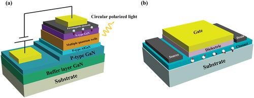
Based on the in-depth research on spin injection, spin relaxation and spin manipulation of the GaN-based semiconductors, some preliminary studies on spintronic devices have been posted. The research of GaN-based semiconductor spintronic devices can be divided into optoelectronic devices and pure electrical devices. The optoelectronic devices include spin-LEDs and spin-lasers, and pure electrical devices are mainly about SFETs [Citation7].
Spin-LEDs of blue and shorter wavelength bands can be fabricated in GaN-based semiconductors due to its wide-bandgap [Citation84,Citation85]. The schematic of Spin-LEDs is shown in . However, the light hole band and the heavy hole band of GaN are degenerate at room temperature, resulting in the theoretical upper limit of the circular polarization of surface-emitting spin-LEDs being only 3% [Citation104]. To solve this problem, researchers have proposed the following solutions. The first solution is to incorporate semi-metal Fe3O4 nanoparticles into GaN light emitting quantum well disks [Citation105]. Due to the different effective masses of light and heavy holes, heavy holes are easier to accumulate in the active region of spin-LEDs, while light holes leave the active region quickly through Fe3O4 nanoparticles. The spatial separation of the light and heavy holes enables the circular polarization of the output light to be higher. The second solution is to fabricate side-emitting GaN-based spin-LEDs, where the upper limit of the circular polarization is higher than 30% [Citation104]. Meanwhile, the degeneracy of heavy hole and light hole bands can be lifted due to the quantum confinement effect based on the ultrathin InGaN quantum wells at room temperature [Citation93,Citation106]. The circular polarization could reach up to 9.2% in this device.
Figure 13. (a) The schematic of Spin-LEDs based on GaN. The ferromagnetic electrode injects the spin polarized carriers into the N-type GaN. Then the polarized electrons recombine with the holes in multiple quantum wells to emit circular polarized light. The P-type AlGaN layer is used as an electron-blocking layer. (b) The schematic of Datta-Das type SFET. The source and drain are both ferromagnetic electrodes (such as Co, Fe, diluted magnetic semiconductors, etc.) for the purpose of injecting and detecting the spin polarized carriers, respectively. The spin orientation can be controlled by the gate electric field instead of the external magnetic field.
Spin lasers can be utilized for applications such as reconfigurable optical interconnects, ultrafast optical switches, and telecommunications with enhanced bandwidth. Y. F. Chen et al. demonstrated a spin laser with circular polarization of 28.2% through the coupling between semi-metal Fe3O4 nanoparticles and GaN nanorods under an external magnetic field of 0.35 T at room temperature [Citation107]. In 2017, the FeCo/MgO spin tunneling junction was used to realize the room temperature spin polariton diode laser based on the bulk GaN [Citation108]. The FeCo is in-plane magnetization that enables the edge-emitting geometry of the spin-laser. Unlike usual GaN UV-LEDs, the N-type GaN layer is on the top of the diode, which aims to reduce the transport length of the spin-polarized electrons. Under the external magnetic field of 1.6 kOe, this spin polariton diode laser could emit up to 25% circularly polarized laser light at room temperature [Citation108].
As shown in , the SFET is an electronic analog of an electro-optical modulator for photons. The injected spin precesses during the transport of the spin-polarized electrons. The spin precession length is modulated by gate voltage, and thus the drain could detect the spin orientation varied artificially.
In previous years, H. C. Koo et al. successfully fabricated the SFETs in the InAs heterostructures at low temperature [Citation4,Citation47,Citation48]. The van der Waals heterostructure Graphene/WS2 achieved the spin precession output signals at room temperature due to its high mobility [Citation109]. Currently, four-terminal spin valves were successfully realized at room temperature by using bulk GaN and GaN nanowires as spin transport channels [Citation91,Citation93,Citation99,Citation100]. The GaN-based semiconductor SFETs need to be further explored due to the lack of gate-controlled spin manipulation.
A non-ballistic transport SFET design is derived from the Datta-Das type SFET [Citation110]. In the case where the two ferromagnetic electrodes are magnetized in the same direction, the spin-polarized electrons that maintain the SU(2) group symmetry will result in lower channel resistance than the unpolarized electrons [Citation49,Citation103,Citation110,Citation111]. InGaN/GaN quantum wells have been verified to have the potential to realize non-ballistic transport SFETs [Citation51]. In order to realize the aim that the spin operator is a conserved quantity, the spin-orbit coupling in the channel needs to be artificially adjusted to 0, which means that is equal to −1. Researchers achieved a − 0.81 ratio in InGaN/GaN quantum wells and proposed some artificial regulation methods to optimize this ratio [Citation51].
7 Conclusion
The development of GaN-based semiconductor spintronic devices with high operating speed, low power consumption and high integration is one of the paths to break through the scaling limit of conventional CMOS. So far, GaN-based spintronics has produced a lot of break throughs in the research of spin relaxation dynamics, spin injection, and spin manipulation. In order to further realize high performance spintronic devices, the efficient injection of electron spins, the controllable extension of spin relaxation time and the gate-controlled spin manipulation are all important research directions. GaN-based high mobility heterostructures (quantum wells) and quantum confined NWs also provide new platforms for the design of spintronic devices.
At the same time, the TRKR measurements and magnetotransport spin valve measurements can extract spin relaxation time, spin diffusion length and spin-injection polarization in detail, thus providing a strong scientific basis for the realization of novel spintronic devices. The development of GaN-based semiconductor spintronic devices is also facing challenges. The efficiency of spin injection needs to be further improved and the gate-voltage-modulation of spin-orbit coupling in GaN-based semiconductors has not yet been realized.
In short, the realization of high-performance room temperature GaN-based spintronic devices still requires in-depth exploration of spin dynamics, further optimization of spin injection, and effective realization of gate-controlled spin manipulation. Once these problems are solved, combined with the excellent optical and electrical properties of GaN-based semiconductors, GaN-based spintronic devices will have good application prospects in spin logic devices, quantum memory devices, and quantum computing etc.
Disclosure statement
No potential conflict of interest was reported by the author(s).
Additional information
Funding
References
- Thompson SE, Parthasarathy S. Moore’s law: the future of Si microelectronics. Mater Today. 2006;9:20–29.
- Wunderlich J, Park B-G, Irvine AC, et al. Spin Hall effect transistor. Science. 2010;330:1801–1804.
- Parkin SS, Hayashi M, Thomas L. Magnetic domain-wall racetrack memory. Science. 2008;320:190–194.
- Koo HC, Kwon JH, Eom J, et al. Control of spin precession in a spin-injected field effect transistor. Science. 2009;325:1515–1518.
- Fiederling R, Keim M, Reuscher G, et al. Injection and detection of a spin-polarized current in a light-emitting diode. Nature. 1999;402:787–790.
- Holub M, Shin J, Saha D, et al. Electrical spin injection and threshold reduction in a semiconductor laser. Phys Rev Lett. 2007;98:146603.
- Datta S, Das B. Electronic analog of the electro‐optic modulator. Appl Phys Lett. 1990;56:665–667.
- Fabian J, Žutić I. Spin-polarized current amplification and spin injection in magnetic bipolar transistors. Phys Rev B. 2004;69:115314.
- Zhang S, Tang N, Zhang X, et al. Excitonic effects on electron spin orientation and relaxation in wurtzite GaN. Phys Rev B. 2021;104:125202.
- Jonker B, Park Y, Bennett B, et al. Robust electrical spin injection into a semiconductor heterostructure. Phys Rev B. 2000;62:8180.
- Johnson M, Silsbee R. Spin-injection experiment. Phys Rev B. 1988;37:5326.
- Schmidt G, Ferrand D, Molenkamp L, et al. Fundamental obstacle for electrical spin injection from a ferromagnetic metal into a diffusive semiconductor. Phys Rev B. 2000;62:R4790.
- Ohno H. Making nonmagnetic semiconductors ferromagnetic. science. 1998;281:951–956.
- Rashba E. Theory of electrical spin injection: tunnel contacts as a solution of the conductivity mismatch problem. Phys Rev B. 2000;62:R16267.
- Fert A, Jaffres H. Conditions for efficient spin injection from a ferromagnetic metal into a semiconductor. Phys Rev B. 2001;64:184420.
- Motsnyi V, De Boeck J, Das J, et al. Electrical spin injection in a ferromagnet/tunnel barrier/semiconductor heterostructure. Appl Phys Lett. 2002;81:265–267.
- Motsnyi VF, Van Dorpe P, Van Roy W, et al. Optical investigation of electrical spin injection into semiconductors. Phys Rev B. 2003;68:245319.
- Fang C, Wan C, Yang B, et al. Determination of spin relaxation times in heavy metals via second-harmonic spin injection magnetoresistance. Phys Rev B. 2017;96:134421.
- Huang L, Wu H, Liu P, et al. Room temperature spin injection into SiC via Schottky barrier. Appl Phys Lett. 2018;113:222402.
- Hanbicki A, Van’t Erve O, Magno R, et al. Analysis of the transport process providing spin injection through an Fe/AlGaAs Schottky barrier. Appl Phys Lett. 2003;82:4092–4094.
- Hanbicki AT, Jonker B, Itskos G, et al. Efficient electrical spin injection from a magnetic metal/tunnel barrier contact into a semiconductor. Appl Phys Lett. 2002;80:1240–1242.
- Tran M, Jaffrès H, Deranlot C, et al. Enhancement of the spin accumulation at the interface between a spin-polarized tunnel junction and a semiconductor. Phys Rev Lett. 2009;102:036601.
- Jain A, Rojas-Sanchez J-C, Cubukcu M, et al. Crossover from spin accumulation into interface states to spin injection in the germanium conduction band. Phys Rev Lett. 2012;109:106603.
- Txoperena O, Song Y, Qing L, et al. Impurity-assisted tunneling magnetoresistance under a weak magnetic field. Phys Rev Lett. 2014;113:146601.
- Lu Y, Tran M, Jaffrès H, et al. Spin-polarized inelastic tunneling through insulating barriers. Phys Rev Lett. 2009;102:176801.
- Dash SP, Sharma S, Le Breton J, et al. Spin precession and inverted Hanle effect in a semiconductor near a finite-roughness ferromagnetic interface. Phys Rev B. 2011;84:054410.
- Sato S, Nakane R, Tanaka M. Origin of the broad three-terminal Hanle signals in Fe/SiO2/Si tunnel junctions. Appl Phys Lett. 2015;107:032407.
- Matsuyama T, Kürsten R, Meißner C, et al. Rashba spin splitting in inversion layers on p-type bulk InAs. Phys Rev B. 2000;61:15588.
- Lamari S. Rashba effect in inversion layers on p-type InAs MOSFET’s. Phys Rev B. 2001;64:245340.
- Teraguchi N, Suzuki A, Nanishi Y, et al. Room-temperature observation of ferromagnetism in diluted magnetic semiconductor GaGdN grown by RF-molecular beam epitaxy. Solid State Commun. 2002;122:651–653.
- Dhar S, Brandt O, Ramsteiner M, et al. Colossal magnetic moment of Gd in GaN. Phys Rev Lett. 2005;94:037205.
- Reed M, El-Masry N, Stadelmaier H, et al. Room temperature ferromagnetic properties of (Ga, Mn) N. Appl Phys Lett. 2001;79:3473–3475.
- Elliott RJ. Theory of the effect of spin-orbit coupling on magnetic resonance in some semiconductors. Phys Rev. 1954;96:266.
- Dyakonov M, Perel V. Spin relaxation of conduction electrons in noncentrosymmetric semiconductors. Soviet Physics Solid State, Ussr. 1972;13:3023–3026.
- Bir G, Aronov A, Pikus G. Spin relaxation of electrons due to scattering by holes. Zh Eksp Teor Fiz. 1975;69:1382–1397.
- Fabian J, Matos-Abiague A, Ertler C, et al. Semiconductor spintronics. Acta Physica Slovaca. 2007;57. 565–907.
- Buß J, Rudolph J, Natali F, et al. Temperature dependence of electron spin relaxation in bulk GaN. Phys Rev B. 2010;81:155216.
- Beschoten B, Johnston-Halperin E, Young D, et al. Spin coherence and dephasing in GaN. Phys Rev B. 2001;63:121202.
- Rudolph J, Buß JH, Hägele D. Electron spin dynamics in GaN. Phys Status Solidi B. 2014;251:1850–1860.
- Krishnamurthy S, Van Schilfgaarde M, Newman N. Spin lifetimes of electrons injected into GaAs and GaN. Appl Phys Lett. 2003;83:1761–1763.
- Buss JH, Rudolph J, Natali F, et al. Anisotropic electron spin relaxation in bulk GaN. Appl Phys Lett. 2009;95:192107.
- Banerjee A, Dogan F, Heo J, et al. Spin relaxation in InGaN quantum disks in GaN nanowires. Nano Lett. 2011;11:5396–5400.
- Nitta J, Akazaki T, Takayanagi H, et al. Gate control of spin-orbit interaction in an inverted In0.53Ga0.47As/In0.52Al0.48 as heterostructure. Phys Rev Lett. 1997;78:1335–1338.
- Furthmeier S, Dirnberger F, Gmitra M, et al. Enhanced spin–orbit coupling in core/shell nanowires. Nat Commun. 2016;7:1–7.
- Yokota N, Aoshima Y, Ikeda K, et al. Room temperature spin transport in undoped (110) GaAs/AlGaAs quantum wells. Appl Phys Lett. 2014;104:072406.
- Chuang P, S-C H, Smith LW, et al. All-electric all-semiconductor spin field-effect transistors. Nat Nanotechnol. 2015;10:35–39.
- Choi WY, H-j K, Chang J, et al. Electrical detection of coherent spin precession using the ballistic intrinsic spin Hall effect. Nat Nanotechnol. 2015;10:666–670.
- Choi WY, H-j K, Chang J, et al. Ferromagnet-free all-electric spin Hall transistors. Nano Lett. 2018;18:7998–8002.
- Balocchi A, Duong Q, Renucci P, et al. Full electrical control of the electron spin relaxation in GaAs quantum wells. Phys Rev Lett. 2011;107:136604.
- Wang G, Liu B, Balocchi A, et al. Gate control of the electron spin-diffusion length in semiconductor quantum wells. Nat Commun. 2013;4:2372.
- Liu X, Tang N, Zhang S, et al. Effective manipulation of spin dynamics by polarization electric field in InGaN/GaN quantum wells at room temperature. Adv Sci. 2020;7:1903400.
- He X, Shen B, Tang Y, et al. Circular photogalvanic effect of the two-dimensional electron gas in AlxGa1−xN∕GaN heterostructures under uniaxial strain. Appl Phys Lett. 2007;91:071912.
- Yin C, Shen B, Zhang Q, et al. Rashba and Dresselhaus spin-orbit coupling in GaN-based heterostructures probed by the circular photogalvanic effect under uniaxial strain. Appl Phys Lett. 2010;97:181904.
- Fu J, Wu M. Spin-orbit coupling in bulk ZnO and GaN. J Appl Phys. 2008;104:093712.
- Stefanowicz W, Adhikari R, Andrearczyk T, et al. Experimental determination of Rashba spin-orbit coupling in wurtzite n-GaN: si. Phys Rev B. 2014;89:205201.
- Majewski JA, Vogl P, Menéndez J, Van de Walle CG, editors. Field dependence of spin lifetimes in nitride heterostructures. Physics of Semiconductors: 27th International Conference on the Physics of Semiconductors; Flagstaff, Arizona. New York: American Institute of Physics; 2005. 772, 1403–1404. doi:10.1063/1.1994639.
- Voon LLY, Willatzen M, Cardona M, et al. Terms linear in k in the band structure of wurtzite-type semiconductors. Phys Rev B. 1996;53:10703–10714.
- Lo I, Wang W, Gau M, et al. Wurtzite structure effects on spin splitting in GaN∕AlN quantum wells. Phys Rev B. 2005;72:245329.
- Silva Ead A. Conduction-subband anisotropic spin splitting in III-V semiconductor heterojunctions. Phys Rev B. 1992;46:1921–1924.
- Fu J, Penteado PH, Candido DR, et al. Spin-orbit coupling in wurtzite heterostructures. Phys Rev B. 2020;101:134416.
- Tang N, Shen B, Han K, et al. Zero-field spin splitting in AlxGa1−xN/GaN heterostructures with various Al compositions. Appl Phys Lett. 2008;93:172113.
- Tang N, Shen B, X-W H, et al. Influence of the illumination on the beating patterns in the oscillatory magnetoresistance in AlxGa1−xN∕GaN heterostructures. Phys Rev B. 2007;76:155303.
- Liu X, Guan H, Tang N, et al. Interfacial symmetry breaking induced spin-orbit coupling in wurtzite GaN nanowires. Appl Phys Lett. 2021;118:122104.
- Buß J, Fernández-Garrido S, Brandt O, et al. Electron spin dynamics in mesoscopic GaN nanowires. Appl Phys Lett. 2019;114:092406.
- Buß J, Rudolph J, Starosielec S, et al. Dyakonov-Perel electron spin relaxation in a wurtzite semiconductor: from the nondegenerate to the highly degenerate regime. Phys Rev B. 2011;84:153202.
- Wolos A, Wilamowski Z, Piersa M, et al. Properties of metal-insulator transition and electron spin relaxation in GaN: si. Phys Rev B. 2011;83:165206.
- Rudolph J, Buß J, Semond F, et al., editors. Dyakonov-perel electron spin relaxation in a highly degenerate wurtzite semiconductor. Physics of Semiconductors: 31th International Conference on the Physics of Semiconductors, Zurich, Switzerland; 2013.1566 Ihn, T, Rossler, C, Kozikov, A. New York: American Institute of Physics, 361–362. doi:10.1063/1.4848435.
- Hu C, Morita K, Sanada H, et al. Spin precession of holes in wurtzite GaN studied using the time-resolved Kerr rotation technique. Phys Rev B. 2005;72:121203.
- Zhang S, Tang N, Liu X, et al. Spin dynamics in GaN/Al0. 1Ga 0. 9N quantum well with complex band edge structure. Appl Phys Lett. 2021;118:252107.
- Zhang S, Tang N, Zhang X, et al. Spin relaxation induced by interfacial effects in GaN/Al0. 25Ga 0. 75N heterostructures. Fundamental Research. 2021; 1: 656–660.
- Kammermeier M, Wenk P, Dirnberger F, et al. Spin relaxation in wurtzite nanowires. Phys Rev B. 2018;98:035407.
- Calarco R, Stoica T, Brandt O, et al. Surface-induced effects in GaN nanowires. J Mater Res. 2011;26:2157–2168.
- Armstrong A, Li Q, Lin Y, et al. GaN nanowire surface state observed using deep level optical spectroscopy. Appl Phys Lett. 2010;96:163106.
- Pfüller C, Brandt O, Grosse F, et al. Unpinning the Fermi level of GaN nanowires by ultraviolet radiation. Phys Rev B. 2010;82:045320.
- Carter DJ, Stampfl C. Atomic and electronic structure of single and multiple vacancies in GaN nanowires from first-principles. Phys Rev B. 2009;79:195302.
- Kroutvar M, Ducommun Y, Heiss D, et al. Optically programmable electron spin memory using semiconductor quantum dots. Nature. 2004;432:81–84.
- He X, Shen B, Chen Y, et al. Anomalous photogalvanic effect of circularly polarized light incident on the two-dimensional electron gas in AlxGa1−xN/GaN heterostructures at room temperature. Phys Rev Lett. 2008;101:147402.
- Yin C, Tang N, Zhang S, et al. Observation of the photoinduced anomalous Hall effect in GaN-based heterostructures. Appl Phys Lett. 2011;98:122104.
- Ohno Y, Young D, Beschoten B, et al. Electrical spin injection in a ferromagnetic semiconductor heterostructure. Nature. 1999;402:790–792.
- Van Dorpe P, Liu Z, Van Roy W, et al. Very high spin polarization in GaAs by injection from a (Ga, Mn) As Zener diode. Appl Phys Lett. 2004;84:3495–3497.
- Jungwirth T, Sinova J, Mašek J, et al. Theory of ferromagnetic (III, Mn) V semiconductors. Rev Mod Phys. 2006;78:809–864.
- Dietl T, oH O, aF M, et al. Zener model description of ferromagnetism in zinc-blende magnetic semiconductors. science. 2000;287:1019–1022.
- Sonoda S, Shimizu S, Sasaki T, et al. Molecular beam epitaxy of wurtzite (Ga, Mn) N films on sapphire (0 0 0 1) showing the ferromagnetic behaviour at room temperature. J Crystal Growth. 2002;237:1358–1362.
- Banerjee D, Adari R, Sankaranarayan S, et al. Electrical spin injection using GaCrN in a GaN based spin light emitting diode. Appl Phys Lett. 2013;103:242408.
- Ham M-H, Yoon S, Park Y, et al. Electrical spin injection from room-temperature ferromagnetic (Ga, Mn) N in nitride-based spin-polarized light-emitting diodes. J Phys. 2006;18:7703–7708.
- Jedema F, Heersche H, Filip A, et al. Electrical detection of spin precession in a metallic mesoscopic spin valve. Nature. 2002;416:713–716.
- Johnson M, Silsbee R. Thermodynamic analysis of interfacial transport and of the thermomagnetoelectric system. Phys Rev B. 1987;35:4959–4972.
- Van’t Erve O, Hanbicki A, Holub M, et al. Electrical injection and detection of spin-polarized carriers in silicon in a lateral transport geometry. Appl Phys Lett. 2007;91:212109.
- Johnson M, Silsbee RH. Interfacial charge-spin coupling: injection and detection of spin magnetization in metals. Phys Rev Lett. 1985;55:1790–1793.
- Jahangir S, Doğan F, Kum H, et al. Spin diffusion in bulk GaN measured with MnAs spin injector. Phys Rev B. 2012;86:035315.
- Bhattacharya A, Baten MZ, Bhattacharya P. Electrical spin injection and detection of spin precession in room temperature bulk GaN lateral spin valves. Appl Phys Lett. 2016;108:042406.
- Liu X, Tang N, Fang C, et al. Spin relaxation induced by interfacial effects in n-GaN/MgO/Co spin injectors. RSC Adv. 2020;10:12547–12553.
- Song A, Chen J, Lan J, et al. Modulating room temperature spin injection into GaN towards the high-efficiency spin-light emitting diodes. Appl Phys Express. 2020;13:043006.
- Ibbetson JP, Fini P, Ness K, et al. Polarization effects, surface states, and the source of electrons in AlGaN/GaN heterostructure field effect transistors. Appl Phys Lett. 2000;77:250–252.
- Liu G, Wu J, Lu Y, et al. A theoretical calculation of the impact of GaN Cap and AlxGa1-xN barrier thickness fluctuations on two-dimensional electron gas in a GaN/AlxGa1-xN/GaN heterostructure. IEEE Trans Electron Devices. 2011;58:4272–4275.
- Deen DA, Storm DF, Scott Katzer D, et al. Suppression of surface-originated gate lag by a dual-channel AlN/GaN high electron mobility transistor architecture. Appl Phys Lett. 2016;109:063504.
- Crespo A, Bellot MM, Chabak KD et al . High-Power Ka-Band Performance of AlInN/GaN HEMT With 9.8-nm-Thin Barrier. IEEE Electron Device Lett. 2010;31:2–4.
- Zhang X, Tang N, Yang L, et al. Electrical spin injection into the 2D electron gas in AlN/GaN heterostructures with ultrathin AlN tunnel barrier. Adv Funct Mater. 2021;31:2009771.
- Kum H, Heo J, Jahangir S, et al. Room temperature single GaN nanowire spin valves with FeCo/MgO tunnel contacts. Appl Phys Lett. 2012;100:182407.
- Park T-E, Park YH, Lee J-M, et al. Large spin accumulation and crystallographic dependence of spin transport in single crystal gallium nitride nanowires. Nat Commun. 2017;8:15722.
- Ambacher O, Smart J, Shealy J, et al. Two-dimensional electron gases induced by spontaneous and piezoelectric polarization charges in N-and Ga-face AlGaN/GaN heterostructures. J Appl Phys. 1999;85:3222–3233.
- Harmon N, Putikka W, Joynt R. Prediction of extremely long mobile electron spin lifetimes at room temperature in wurtzite semiconductor quantum wells. Appl Phys Lett. 2011;98:073108.
- Wang W-T, Wu C, Chiang J, et al. Spin-degenerate surface and the resonant spin lifetime transistor in wurtzite structures. J Appl Phys. 2010;108:083718.
- Bhattacharya A, Baten Z, Frost T, et al. Room temperature GaN-based edge-emitting spin-polarized light emitting diode. IEEE Photonics Technol Lett. 2017;29:338–341.
- Chen J, Ho C, Lu M, et al. Efficient spin-light emitting diodes based on InGaN/GaN quantum disks at room temperature: a new self-polarized paradigm. Nano Lett. 2014;14:3130–3137.
- Wu Y, Wu X, Zhong Z, et al. Room-temperature spin injection and optical polarization in nitride-based blue and ultra-violet spin light-emitting diodes. Appl Phys Express. 2020;13:123001.
- Chen J-Y, Wong T-M, Chang C-W, et al. Self-polarized spin-nanolasers. Nat Nanotechnol. 2014;9:845–850.
- Bhattacharya A, Baten MZ, Iorsh I, et al. Room-temperature spin polariton diode laser. Phys Rev Lett. 2017;119:067701.
- Afzal AM, Khan MF, Eom J. Gate-Voltage-Modulated Spin Precession in Graphene/WS2 Field-Effect Transistors. Electronics. 2021;10:2879.
- Schliemann J, Egues JC, Loss D. Nonballistic spin-field-effect transistor. Phys Rev Lett. 2003;90:146801.
- Cartoixa X, Ting D-Y, Chang Y-C. A resonant spin lifetime transistor. Appl Phys Lett. 2003;83:1462–1464.