
ABSTRACT
Color centers in hexagonal boron nitride (hBN) have recently emerged as promising candidates for a new wave of quantum applications. Thanks to hBN’s high stability and two-dimensional (2D) layered structure, color centers in hBN can be readily integrated into nanophotonic and plasmonic structures on a chip. More importantly, the recently discovered optically addressable spin defects in hBN provide a quantum interface between photons and electron spins for quantum sensing applications. The most well-studied hBN spin defects, the negatively charged boron vacancy () spin defects, have been used for quantum sensing of static magnetic fields, magnetic noise, temperature, strain, nuclear spins, paramagnetic spins in liquids, RF signals, and beyond. In particular, hBN nanosheets with spin defects can form van der Waals (vdW) heterostructures with other 2D materials for in situ quantum sensing and imaging. This review summarizes the rapidly evolving field of quantum sensing with spin defects in hBN. We introduce basic properties of hBN spin defects, quantum sensing protocols, and recent experimental demonstrations of quantum sensing and imaging with hBN spin defects. We also discuss methods to enhance their sensitivity. Finally, we envision some potential developments and applications of hBN spin defects.
GRAPHICAL ABSTRACT
1. Introduction
Quantum sensing encompasses a diverse range of devices that utilize their quantum properties to detect various weak signals [Citation1,Citation2]. These devices can achieve high accuracy, stability, and resolution surpassing the performance of classical approaches. So far, a diverse range of quantum platforms, including atomic, photonic, and solid-state systems [Citation3–5], have demonstrated promising performance for quantum sensing applications. In particular, solid-state spin defects have broad applications in condensed matter physics, materials science, biology, and other fields [Citation6–12].
Point defects in solids are analogues of atomic systems ‘trapped’ in their host materials. Some point defects exhibit unique optical and spin properties, leading to applications in quantum science and technology. To date, spin color centers in diamond and silicon carbide have been extensively studied [Citation13–17]. In particular, diamond nitrogen-vacancy (NV) centers are currently the most widely used solid-state system for quantum sensing applications [Citation4,Citation18,Citation19]. Diamond NV centers have great stability and sensitivity to multiple physical quantities over a broad range of probing conditions. They also have large contrasts in optically detected magnetic resonance (ODMR) and long spin coherence time at room temperature [Citation20–23]. However, one of the drawbacks of diamond is the difficulty in creating high-quality NV centers near the diamond surface due to surface charge and spin noises [Citation24–26]. It is also challenging to fabricate diamond nanostructures and integrate them with other materials. These issues severely limit their applications when close proximity to the target sample is required. Such limitations originate from the dangling bonds on the surface of a three-dimensional (3D) diamond and cannot be fully avoided with diamond.
In this context, quantum defects in two-dimensional (2D) van de Waals (vdW) materials offer new opportunities to address these limitations [Citation39–42]. 2D vdW materials can be stable even at the monolayer limit and essentially have no dangling bonds on the surface, which effectively avoids the problems encountered by diamond surfaces. Furthermore, 2D vdW materials can form multifunctional heterostructures, which open prospects for in situ quantum sensing [Citation43]. So far, quantum defects have been discovered in two major classes of 2D materials: hexagonal boron nitride (hBN) [Citation44–48] and transition metal dichalcogenides [Citation49–52]. In particular, hBN has recently emerged as a promising material for nanoscale quantum sensing. A monolayer hBN has a structure similar to that of graphene but consists of alternating boron and nitrogen atoms. hBN has a unique combination of a wide band gap ( 6 eV) [Citation53], high thermal conductivity, and excellent chemical and mechanical stability, making it well-suited for use in various sensing conditions where traditional sensing methods may be unreliable [Citation53–56]. The large band gap of hBN enables numerous defect energy states within the band gap, which give rise to many different optically active defect centers with optical spectra ranging from near-infrared to ultraviolet [Citation44,Citation46,Citation57–61].
In 2020, ODMR of spin defects in hBN was reported [Citation27]. Since then, several types of optically active spin defects in hBN have been observed [Citation27,Citation62–65], with the negatively charged boron vacancy () spin defect being the most extensively studied. Many recent studies demonstrated its promising potential as a new platform for quantum sensing [Citation66]. The spin states of
spin defects can be initialized with a green laser, controlled by a microwave, and read out by their photoluminescence under green laser excitation.
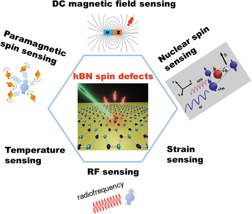
The hBN spin defects can be used to probe external perturbations with high sensitivity [Citation29,Citation31]. Their advantage is that these defects are highly stable, residing within a few layers of the material [Citation44,Citation64]. They provide an opportunity to achieve much closer and stronger interactions with the target sample to be monitored. In materials science and condensed matter physics, they promise high-resolution imaging of magnetic fields [Citation67,Citation68], which may arise from 2D magnetic materials, superconductors, and other spin-based devices. spin defects are also sensitive to other physical quantities. Researchers have used hBN
spin defects for sensing a broad range of quantities (), including static magnetic fields [Citation29,Citation30], high-frequency magnetic noise due to spin fluctuations in solids [Citation30], temperature [Citation31,Citation32], strain [Citation33,Citation34], nuclear spins [Citation37], paramagnetic spins in liquids [Citation35,Citation36], and RF signals [Citation38].
Figure 1. An overview of quantum sensing with spin defects in hBN. spin defects in hBN have been used to measure the DC magnetic field [Citation27–30], temperature [Citation31,Citation32], strain [Citation33,Citation34], paramagnetic spins in liquids [Citation35,Citation36], nuclear spins [Citation37], RF signals [Citation38], and etc. This figure is created from results reported in [Citation27,Citation29,Citation34,Citation36,Citation37]. Copyright by Springer Nature [Citation27,Citation29,Citation37] and American Chemical Society [Citation34]. The center illustration of an hBN spin defect is created by Zhujing Xu.
![Figure 1. An overview of quantum sensing with spin defects in hBN. spin defects in hBN have been used to measure the DC magnetic field [Citation27–30], temperature [Citation31,Citation32], strain [Citation33,Citation34], paramagnetic spins in liquids [Citation35,Citation36], nuclear spins [Citation37], RF signals [Citation38], and etc. This figure is created from results reported in [Citation27,Citation29,Citation34,Citation36,Citation37]. Copyright by Springer Nature [Citation27,Citation29,Citation37] and American Chemical Society [Citation34]. The center illustration of an hBN spin defect is created by Zhujing Xu.](/cms/asset/1a9fe51d-9ed6-4d9d-8d67-157825356615/tapx_a_2206049_f0001_oc.jpg)
This review primarily focuses on the spin defects in hBN and their applications in sensing (). For an overview of different spin defects, readers can refer to a recent review by Liu et al. [Citation69]. In the following sections, this paper is organized as follows. We first briefly review the properties of the
spin defects and some other spin-active hBN defects in section 2. In Section 3, we discuss basic principles of quantum sensing using hBN spin defects, including the spin Hamiltonian, the sensing protocols, and the sensitivity of this system. Section 4 covers the applications of hBN spin defects in magnetic imaging, temperature sensing, strain sensing, nuclear magnetic resonance (NMR) detection, liquid paramagnetic spin sensing, and RF sensing. We then discuss ways to improve sensitivity in Section 5 and conclude in Section 6 by envisioning future developments in quantum sensing with hBN spin defects.
2. Spin defects in hBN
Optically addressable spin defects offer an interface between photons and electron spin states, which are highly sought after for quantum information applications. In hBN, paramagnetic defects were first measured using conventional electron paramagnetic resonance (EPR) in 1970s [Citation70–72]. Only in the last few years, optically addressable spin defects were observed in hBN [Citation27,Citation62–64,Citation73]. In this section, we discuss the basic properties of spin defects in hBN and techniques for creating the desired spin defects.
2.1. Creation of spin defects
Since the discovery of optically addressable spin defects in hBN [Citation27], several experimental approaches have been developed to deterministically create spin defects. To generate defects, the basic idea is to knock out the boron atoms from the hBN lattice (). There are many available methods, including neutron irradiation [Citation27,Citation77–79], ion implantation (including focused ion beam) [Citation28,Citation76,Citation80,Citation81], electron beam irradiation [Citation82] and femtosecond laser writing [Citation74] ( (a)-(b)). Neutron irradiation was the first method used to create
[Citation27,Citation78]. Indeed,
is among the materials with the highest neutron absorption cross-sections and is commonly used as a neutron absorber. The thermal neutrons have a much higher probability to react with boron atoms than nitrogen atoms, which causes fission and leaves mostly boron vacancies () with a high production efficiency [Citation83]. However, this method requires a nuclear reactor with a high thermal flux density, which is hardly accessible. Femtosecond laser writing is a cheaper and more flexible method as it can be operated in an ambient condition [Citation74]. However, the spin defect generation process is associated with crystal damage, which has yet to be addressed. High-energy electron irradiation uses a high-energy (
2 MeV) electron beam to break the chemical bonds, which is a robust way to create
defects without greatly damaging the hBN crystals [Citation82]. Ion implantation is so far the most widely used way for generating
defects, owing to its convenience and ease of access. Many different species of ions can be used to create
defects, including H+ [Citation84], He+ [Citation28,Citation80], C+ [Citation80,Citation81], N+ [Citation76,Citation80], Ar+ [Citation76,Citation80], Ga+ [Citation76], and Xe+ [Citation76] ions. The
defects can be generated at different depth by changing the ion energies. The depth as well as the distribution of generated
defects can be estimated by Stopping and Range of Ions in Matter (SRIM) simulation [Citation85]. For example, the average depth of defects generated by a 2.5 keV He+ ion beam is about 25 nm [Citation28]. A focused ion beam can pattern an array of
defects with controllable dose densities and positions [Citation76], as shown in . Thermal treatment during or after ion implantation is also demonstrated to help improve the spin properties of
defects [Citation86]. Suzuki et al. performed ion implantation at high temperatures and demonstrated that the ODMR contrast of the created spin defects increased with an increasing temperature [Citation86]. Such an improvement saturated at around 500°C.
Figure 2. (a) Creation of spin defects via femtosecond laser writing. Reproduced from [Citation74]. Copyright of American Chemical Society. (b) Creation of
spin defects via ion, electron or neutron irradiation. (c) a TEM image of a boron vacancy defect in an hBN 2D lattice. The scale bar is 0.2 nm. Reproduced from [Citation75]. Copyright by American Physical Society. (d) an optical image of an exfoliated hBN flake after ion implantation with a focused ion beam. The inset shows a PL map of the patterned area. The scale bar is 20
m. Reproduced from [Citation76]. Copyright by American Chemical Society.
![Figure 2. (a) Creation of spin defects via femtosecond laser writing. Reproduced from [Citation74]. Copyright of American Chemical Society. (b) Creation of spin defects via ion, electron or neutron irradiation. (c) a TEM image of a boron vacancy defect in an hBN 2D lattice. The scale bar is 0.2 nm. Reproduced from [Citation75]. Copyright by American Physical Society. (d) an optical image of an exfoliated hBN flake after ion implantation with a focused ion beam. The inset shows a PL map of the patterned area. The scale bar is 20 m. Reproduced from [Citation76]. Copyright by American Chemical Society.](/cms/asset/5ef10628-ae66-4ca4-ac2e-4dbe48e609c9/tapx_a_2206049_f0002_oc.jpg)
Besides spin defects, there have been efforts to create other spin defects which can be brighter. So far, there have been a few successful approaches to create those spin defects beyond
[Citation62–64]. By incorporating carbon atoms during the growth phase of the hBN crystal during the metal-organic vapor-phase epitaxy (MOVPE) and molecular beam epitaxy (MBE), carbon-related spin defects can be created [Citation62,Citation64]. Femtosecond laser writing followed by thermal annealing has also been used to create spin defects in hBN [Citation87]. Despite the potential of these new spin qubits, research in this area is still in its early stages. In this review, we will mainly focus on
spin defects in hBN.
2.2. Negatively charged boron vacancy defects
2.2.1. Electronic structure
In 2018, Toledo et al. observed spin defects in a neutron-irradiated hBN sample through conventional EPR experiments [Citation77]. In 2020, Gottscholl et al. [Citation27] successfully performed ODMR measurements of spin defects in hBN. Shortly after the experimental observation, several theoretical studies [Citation88–92] and excited-state ODMR experiments [Citation81,Citation93–95] helped reveal the atomic and electronic structure of the
defect (). A
defect is formed by a vacant boron site and an additional electron captured from the lattice. It is surrounded by three equivalent nitrogen atoms (). The highest point group symmetry of
is
, which is expected to be reduced to the
symmetry due to the Jahn-Teller distortion [Citation90] or under the effect of an external strain. The electronic structure of the
defect involves ten electrons. Six are provided by the three fully occupied
orbitals of the three nearest nitrogen atoms, and another three are half-filled dangling bonds of the three nearest nitrogen atoms. The tenth electron is captured from the environment, making the overall negatively charged state of
. As depicted in , the spin density of the ground state is mostly located in the plane of the hBN lattice, with the highest density near the three nearest nitrogen atoms.
Figure 3. (a) an energy level schematic of a defect illustrating the electronic ground state, two excited states and a metastable state. Reproduced from [Citation81]. Copyright by American chemical society. (b) Electronic spin density of the
ground state. Reproduced from [Citation37]. Copyright by springer nature. (c) a photoluminescence spectrum of the
defect under 532 nm green laser excitation. Reproduced from [Citation27]. Copyright by springer nature.
![Figure 3. (a) an energy level schematic of a defect illustrating the electronic ground state, two excited states and a metastable state. Reproduced from [Citation81]. Copyright by American chemical society. (b) Electronic spin density of the ground state. Reproduced from [Citation37]. Copyright by springer nature. (c) a photoluminescence spectrum of the defect under 532 nm green laser excitation. Reproduced from [Citation27]. Copyright by springer nature.](/cms/asset/82d5e05f-9814-4e76-a951-4f8991ee853d/tapx_a_2206049_f0003_oc.jpg)
2.2.2. Optical properties
An energy level diagram of the defect is shown in (a). The basic photophysics can be illustrated by three electronic energy levels, including a ground state (GS) of symmetry
, two excited states (ES) of symmetry
and
, as well as a metastable state (MS) with symmetry
() [Citation90]. The
defects can be efficiently excited by light at most wavelengths below 680 nm [Citation76]. Experimentally, a 532 nm green laser is commonly used as the excitation light source for ODMR experiments. At room temperature,
defects exhibit a broad emission spectrum centered near 820 nm without a sharp distinct zero phonon line (ZPL) [Citation96] (). By coupling the hBN layer to a high-Q cavity, Qian et al. measured the room-temperature ZPL to be at 773 nm [Citation97]. At cryogenic temperatures, the photoluminescence (PL) spectrum remains mostly unchanged from the room-temperature spectrum [Citation93]. The lifetime of the excited state is approximately 1.2 ns, which is mainly due to the fast nonradiative decay [Citation27]. So far,
defects suffer from low brightness, and no single photon emission has been observed from a
defect. The low quantum efficiency (
) of
defects is because the transition between the GS and ES triplet subspace is dipole forbidden when strain and electric fields are not considered [Citation88,Citation90].
2.2.3. Spin properties
The electronic ground state of a defect has spin
. The spin polarization of
defects is along the hBN c-axis, that is perpendicular to the 2D-lattice plane [Citation27,Citation88,Citation90]. As shown in , the triplet GS and ES can be further split into three spin sub-levels each. Without an external magnetic field, the dipolar spin-spin interaction gives rise to the fine structures in both GS and ES with longitudinal zero field splitting (ZFS) parameters
3.48 GHz [Citation27] and
2.1 GHz [Citation81,Citation93–95]. Due to the local electric field or strain, the ODMR spectrum also includes transverse ZFS components. The ground state transverse ZFS,
, ranges from 48 MHz to 75 MHz [Citation27,Citation80,Citation93,Citation98], while the excited state transverse ZFS,
, is reported in the range of 93–154 MHz [Citation81,Citation93–95], making the
states slightly non-degenerate [Citation93]. Differences in transverse ZFS components among different samples are due to varying local electric fields, which depend on crystal damage levels and charged defect environments. The latter depends on the density of
ensembles. Both factors are affected by defect creation processes, including doping sources and dosage [Citation80]. In an external magnetic field, the
states are shifted towards opposite directions via Zeeman effect. The spin lifetime
in the ground state is about 18
s at room temperature, and can increase to about 12.5 ms at 20 K [Citation96]. The spin dephasing time
is about 100 ns, while the measured spin coherence time
varies from about 100 ns [Citation79] to about 2
s at room temperature [Citation96]. There is also a metastable state with
which facilitates nonradiative transfer of the spin state from the excited to the ground state. The metastable state is essential for spin polarization and readout.
2.2.4. Optically detected magnetic resonance
To perform ODMR measurements, the spin states are initialized and readout optically using a green laser. The optical cycle in the electronic energy level subspace includes multiple steps (). Under the illumination of a 532 nm laser, the transitions consist of excitation from the GS to the ES
, fast (subpicosecond) relaxation to the ES
, radiative recombination back to the GS
, and nonradiative spin-dependent inter-system crossing (ISC). The spin-dependent ISC process induces the difference in the populations and the PL count rates of different spin states, which is crucial for optical initialization and readout of the spin states (bright state
versus dark states
). The laser excitation and radiative decay channels are spin conservative processes, during which the spin state remains unchanged. Due to different MS
GS/ES transition rates between the
and
states, the defects can be spin polarized to the
state using continuous optical pumping. This enables us to initialize and readout the spin states and perform quantum sensing based on various protocols as described in later sections.
shows the schematic of an ODMR measurement setup involving optical excitation, and microwave drive using a microwave waveguide onto which the hBN flakes are transferred [Citation28]. The objective lens helps focus the excitation laser and collect the PL emission from the defects. An external magnetic field can be applied with a nearby magnet.
Figure 4. (a) an experimental scheme for taking ODMR measurements. (b) ODMR spectra in different magnetic fields: 0 mT, 5.9 mT and 9.8 mT. Reproduced from [Citation28]. copyright by American chemical society. (c) the ground state and excited state ODMR spectrum at 0 magnetic field. Reproduced from [Citation93]. (d) the ground state and excited state ODMR spectrum as a function of magnetic field. Reproduced from [Citation81]. Copyright by American chemical society.
![Figure 4. (a) an experimental scheme for taking ODMR measurements. (b) ODMR spectra in different magnetic fields: 0 mT, 5.9 mT and 9.8 mT. Reproduced from [Citation28]. copyright by American chemical society. (c) the ground state and excited state ODMR spectrum at 0 magnetic field. Reproduced from [Citation93]. (d) the ground state and excited state ODMR spectrum as a function of magnetic field. Reproduced from [Citation81]. Copyright by American chemical society.](/cms/asset/16a4d3df-545e-4ffc-bbe9-646bb5b9fbc1/tapx_a_2206049_f0004_oc.jpg)
A basic ODMR experiment is to record the electron spin resonance (ESR) spectrum of the defects by slowly sweeping the driving microwave frequency over the ESR transitions. A reduction of the PL intensity will be observed when the microwave frequency matches the ESR transition frequency so that the transition between
and
states occurs (). When spin defects are in the presence of an external magnetic field, the transition frequencies shift due to the Zeeman effect () [Citation27,Citation28]. The ODMR experiments can be carried out using a continuous wave (CW) protocol or pulsed microwave measurements. The CW ODMR protocol is widely used in sensing applications as it is technically simple and offers relatively high photon counts. When we sweep the microwave frequency over a large range, both the ground-state and the excited-state transitions are clearly visible, forming two distinct sets of branches in the ODMR spectrum as shown in . By fitting the slope of the transition frequencies versus magnetic fields (), the electron spin Landé g-factor of
can be obtained as g
2, indicating the spin-orbital coupling is very weak [Citation27,Citation93]. ODMR measurements with low microwave powers can also reveal the hyperfine coupling between the electronic spin and the surrounding nitrogen nuclear spins. This coupling results in seven hyperfine peaks in the GS ODMR spectrum, which will be discussed more in Sec. 4.5 [Citation37,Citation96]. The hyperfine splittings have not been resolved in the ES due to the short ES lifetime and inhomogenous broadening in the defect ensemble [Citation81,Citation93–95].
2.3. Other hBN spin defects
While the defect is the most studied hBN spin defect so far, other spin defects in hBN have been demonstrated experimentally. Carbon was identified as a source of a family of defects, and shown to have ODMR signals () [Citation62,Citation64]. By controlling the concentration of carbon impurities, both spin ensembles (with high concentration) () and single spin defects (with low concentration) can be generated. Mendelson et al. generated carbon-related spin defects in hBN by the inclusion of carbon atoms during the metal – organic vapour-phase epitaxy (MOVPE) growth of hBN samples, and demonstrated the room-temperature ODMR in the spin ensembles [Citation62] (). Stern et al. later reported ODMR measurements on single spin defects with the carbon-doped hBN sample, also created by the MOVPE method [Citation64]. The ODMR signal was found to change in sign for different single spin defects, even within the same sample (). Chejanovsky et al. identified a few types of spin defects in hBN flakes, which had been annealed at
C [Citation63]. The ODMR spectra were observed only at cryogenic temperature in [Citation63]. One of those defects has been proposed to be a carbon substitution defect [Citation99]. Recently, Guo et al. reported a room-temperature ultrabright single spin defect with a ZPL around 540 nm [Citation100]. This spin defect exhibits
2.5 MHz count rate under 1 mW green laser excitation, which is much brighter than other reported single spin defects in hBN. All of the hBN single spin defects discussed above exhibit g-factors
2, and have small ZFS (<100 MHz) which often requires an external magnetic field to obtain a clear ODMR signal.
Figure 5. (a) a photoluminescence spectrum of a carbon-related defect in hBN. Inset: measurement demonstrating single-photon emission from a single spin defect. Reproduced from [Citation62]. Copyright by springer nature. (b) ODMR spectra of a carbon-related defect, which demonstrates a shift in the peak as a function of the magnetic field. Reproduced from [Citation62]. Copyright by springer nature. (c) ODMR spectra of two single spin defects and an ensemble. The ODMR spectra of single spin defects can have opposite signs, leading to an overall reduction in the ODMR contrast of an ensemble with different types of spin defects. Reproduced from [Citation64]. .
![Figure 5. (a) a photoluminescence spectrum of a carbon-related defect in hBN. Inset: measurement demonstrating single-photon emission from a single spin defect. Reproduced from [Citation62]. Copyright by springer nature. (b) ODMR spectra of a carbon-related defect, which demonstrates a shift in the peak as a function of the magnetic field. Reproduced from [Citation62]. Copyright by springer nature. (c) ODMR spectra of two single spin defects and an ensemble. The ODMR spectra of single spin defects can have opposite signs, leading to an overall reduction in the ODMR contrast of an ensemble with different types of spin defects. Reproduced from [Citation64]. .](/cms/asset/b363915d-35d4-47a5-832e-c8e27488493e/tapx_a_2206049_f0005_oc.jpg)
In addition, Chen and Quek theoretically predicted a neutrally-charged double-boron-vacancy (VB2) spin defect with a triplet GS [Citation92]. The ZFS parameters were proposed to be GHz and
MHz. Babar et al. experimentally observed this defect via scanning transmission electron microscopy (STEM) [Citation101]. A VB2 defect consists of a pair of adjacent in-plane boron vacancies and a nitrogen atom migrating into one of the vacancy sites. As a result, this forms a VBVNNB complex including a boron vacancy, a nitrogen vacancy, and a nitrogen anti-site. An oxygen related defect has also been identified via conventional EPR and PL spectra simulations and experiments [Citation102]. In addition, Yang et al. reported new types of spin defects in hBN created by femtosecond laser writing and subsequent annealing, but the origins of these defects are still unknown [Citation87]. It has been proposed that carbon trimer substitutional defect is a possible spin defect with single-photon emission around 600 nm [Citation103,Citation104]. A theoretical calculation by Pinilla et al. also predicted that non-adjacent carbon substitutions of the kind
-
or
-
have triplet ground state which may likely be spin defects [Citation105].
3. Quantum sensing with hBN spin defects
Spin defects in hBN show improved versatility for quantum sensing of proximate objects, e.g. 2D magnetic materials. In this section, we introduce the basic principles of quantum sensing using hBN spin defects and related sensing protocols.
3.1. Spin hamiltonian
The ground-state electron spin Hamiltonian of
involves terms with ZFS, electron Zeeman splitting, and electron-nuclear spin hyperfine interaction [Citation27,Citation37,Citation106]:
where GHz is the ground state longitudinal ZFS parameter [Citation27],
MHz is the transverse ZFS parameter [Citation93],
and
(j=x, y, z) are electron spin-1 operators,
28 GHz T−1 is the electron-spin gyromagnetic ratio when the Landé g-factor is
.
(k = 1, 2, 3) is the nuclear spin-1 operator of the three nearest
nuclei, and
is the hyperfine interaction tensor. An important component of the hyperfine interaction tensor is
MHz [Citation37,Citation90,Citation106].
When the external magnetic field is parallel to the
axis, the resonant frequencies of transitions between the
and
states are [Citation27]:
The formula for the excited state is similar, but has different parameters [Citation93]. The experimentally observed ODMR spectrum of is shown in . The slope of the lines correspond to the electron spin gyromagnetic ratio.
Quantum sensing can be performed to measure magnetic field, temperature, strain and pressure via the shift in the ODMR resonance frequency [Citation31]. As seen in , the separation between the two dips in the ODMR spectrum increases when the external magnetic field increases [Citation27,Citation28]. This is due to the different signs of the Zeeman interaction for and
states. The two peaks have Zeeman shifts in opposite directions, yielding a separation of
when
. This enables accurate measurement of magnetic fields. The center of the GS ODMR transition frequencies (
) is proved to be temperature dependent as shown in , which allows temperature sensing based on ODMR experiments [Citation31,Citation32]. The pressure also affects hBN
defects via the ZFS parameter
. By measuring the change of
, one can obtain the ambient pressure with
defects. The coupling constants and reported sensitivities of recent experiments at room temperature are summarized in . The sensor volume in Ref [Citation31]. is relatively large as it used a low NA objective lens and a thick hBN single crystal with low-density spin defects. It can be substantially reduced by using a high NA objective lens and thin hBN nanosheets [Citation28]. For strain sensing, estimated resolutions based on figures reported in [Citation33,Citation34] are listed here since strain sensing sensitivities have not been reported. More details of these experiments will be discussed in Section 4.
Figure 6. (a) Top: Illustration of CW ODMR pulse sequence. Bottom: CW ODMR Spectra of spin defects as a function of temperature and magnetic field [Citation31]. (b) Top: Pulse schematic for the coherent control experiment. A microwave pulse with a variable time duration time is applied between two laser pulses to manipulate the spin state. Bottom: An example of Rabi oscillation [Citation109]. (c) Top: Pulse schematic for the pulsed ODMR measurement. Bottom: An example of pulsed ODMR measurement in a 400 G magnetic field [Citation93]. (d) Top: Pulse schematic for the Ramsey experiment. Bottom: An example result of Ramsey fringes of
defects due to surrounding nuclear spins [Citation110]. (e) Top: Pulse schematic for the spin echo measurement. Bottom: Spin echo measured by using two different microwave driving powers [Citation109]. With a higher microwave Rabi frequency,
shows a better spin coherence. (f) Top: Pulse schematic for relaxometry measurements. The dashed box refers to the application of microwaves during the measurement of the states
and is absent during the measurement of
. Bottom: Normalized photoluminescence of the three spin sublevels as a function of delay time [Citation30]. Reproduced from [Citation30,Citation31,Citation93,Citation109,Citation110].
![Figure 6. (a) Top: Illustration of CW ODMR pulse sequence. Bottom: CW ODMR Spectra of spin defects as a function of temperature and magnetic field [Citation31]. (b) Top: Pulse schematic for the coherent control experiment. A microwave pulse with a variable time duration time is applied between two laser pulses to manipulate the spin state. Bottom: An example of Rabi oscillation [Citation109]. (c) Top: Pulse schematic for the pulsed ODMR measurement. Bottom: An example of pulsed ODMR measurement in a 400 G magnetic field [Citation93]. (d) Top: Pulse schematic for the Ramsey experiment. Bottom: An example result of Ramsey fringes of defects due to surrounding nuclear spins [Citation110]. (e) Top: Pulse schematic for the spin echo measurement. Bottom: Spin echo measured by using two different microwave driving powers [Citation109]. With a higher microwave Rabi frequency, shows a better spin coherence. (f) Top: Pulse schematic for relaxometry measurements. The dashed box refers to the application of microwaves during the measurement of the states and is absent during the measurement of . Bottom: Normalized photoluminescence of the three spin sublevels as a function of delay time [Citation30]. Reproduced from [Citation30,Citation31,Citation93,Citation109,Citation110].](/cms/asset/2bc2a3fd-6db8-486c-81b8-cda8d79f0f2f/tapx_a_2206049_f0006_oc.jpg)
Table 1. Coupling coefficients and reported sensitivities.
3.2. Sensing protocols
In order to measure external fields via shifts in the ODMR signal, a number of protocols [Citation1,Citation111] have been developed and most of them are applicable to the hBN spin defects. The most common protocols are the CW ODMR spectroscopy, pulsed time evolution measurement, and spin relaxometry measurement. Here we briefly explain each of the three methods.
3.2.1. Continuous wave optically detected magnetic resonance
In the CW ODMR protocol, the resonant frequencies of the spectrum are recorded and the shifts are tracked in the presence of external fields () [Citation27,Citation31]. These shifts contain the information of the magnitudes of the external perturbations as per the Hamiltonian discussed in EquationEquation 1(1) . This method does not require pulsed laser excitation, precise microwave manipulation, fast photodetectors, or multichannel pulse generators. Therefore, this method is easy to implement for real sensing applications. shows CW ODMR spectra of hBN
defects as a function of magnetic field and temperature [Citation31]. The resonant frequency shifts with external perturbations, from which the magnitude of the magnetic field or temperature can be calculated.
The smallest possible detectable shift in the resonant frequency of ODMR is [Citation111]
where is the linewidth of the spectrum,
is the optical contrast between the
and
states,
is the detected rate of photons (photon counts per second), and
is the collection time per measurement. This gives a static magnetic field detection sensitivity
[Citation111]:
The sensitivity can be improved by increasing the collected photon count rate and ODMR contrast, as well as narrowing down the ODMR linewidth. These parameters are dependent on laser and microwave powers, and can change oppositely when we tune the laser or microwave powers. Thus there is a trade-off when we optimize the sensitivity. The sensitivity can also be improved by using a larger number of defects by increasing the density of spin defects or increasing the sensor volume. However, increasing the spin density too much could increase the linewidth due to spin-spin interaction. Increasing the sensor volume will reduce the spatial resolution. In addition, spin ensembles usually suffer from inhomogeneous broadening, which may need to be considered for optimizing the ultimate sensitivity of a spin ensemble.
3.2.2. Pulsed measurements
Pulsed measurement is an alternative method that can be more sensitive to certain external perturbations. Pulsed sensing protocols rely on microwave pulses when the laser is turned off during the sensing period. This technique can avoid optical and microwave power broadening, and enable nearly -limited sensitivities in pulsed ODMR and Ramsey measurements [Citation18,Citation112]. By using more complex pulsed sensing protocols, like spin-echo and dynamic decoupling, the sensitivity can be further improved to be limited by
instead of
[Citation18,Citation112]. Three major groups of pulsed sensing protocols are: pulsed-ODMR, Ramsey and spin-echo. All these techniques require precise coherent control of spins.
a) Spin coherent control
Coherent control of spin defects is achieved by applying a microwave pulse of variable length to coherently manipulate the spin state () [Citation96,Citation109,Citation113]. Depending on the frequency of the microwave pulse, we can efficiently couple two spin states, e.g.
. After initializing the spin state to
state with a green laser pulse, a periodically varying magnetic field
(microwave), with orientation perpendicular to the
spin axis and frequency
in resonant with the
transition, can be applied for coherent control. The microwave magnetic field drives the spin to oscillate between the
state and the
state at an angular frequency
, which is the Rabi frequency. This oscillation is also known as the Rabi oscillation. After the microwave pulse, another laser pulse is applied and meanwhile a photon counter records the photon numbers from the spin defects. Since the
and
states have different brightness, the final spin state can be read out based on the collected photon counts. By varying the time duration of the microwave pulse, an oscillation of the PL intensity is observed, from which we can extract the Rabi frequency that will be useful for other pulsed experiments.
b) Pulsed ODMR measurement
In a pulsed ODMR measurement (), we can obtain a spectrum similar to the ground-state part of the CW ODMR but without suffering from optical and microwave broadening. In the pulsed ODMR sensing protocol [Citation18], the spin defects are first optically initialized to state. Then a microwave is applied with a finite duration time
=
. Such a microwave pulse is called a
pulse. Finally, a laser pulse is used to optically readout the final spin state. In the experiment, the microwave frequency is swept across the resonance. At the resonant frequency, the
pulse flips the spin state most precisely from
to
, which gives the highest ODMR contrast. A change in the external field will shift the spin resonance away from the original transition frequency, and thus changes the population transferred to the
state. For the pulsed ODMR, the spectral linewidth is determined by the natural profile of spin transitions and broadening from the duration of the microwave
pulse. Both factors are limited by the spin dephasing time
, which gives a
limited-sensitivity to DC magnetic fields [Citation114]:
where is the photon counting time in each pulse. The contrast
decreases when
is too large. Thus there is an optimal
to achieve the highest sensitivity.
c) Ramsey measurement
Ramsey sequence is another method that is sensitive to static DC magnetic fields () [Citation4]. Similar to the pulsed ODMR technique, the sensitivity of a Ramsey measurement is limited by . The Ramsey experiment also starts with laser initialization to prepare the spin in the
state. Then a resonant microwave field
is applied for a duration
. This is known as a
pulse, which transfer the initial spin state into a superposition state
. This state is then left to precess for a duration of
. If the spin defect is in a DC magnetic field, an additional phase difference
will be accumulated between the
state and the
state. The phase
is proportional to the duration time and the magnitude of the DC field. After the precession period, a second
pulse is applied to map the phase
onto a population difference between the
state and the
state, which will be readout optically by using a second laser pulse. As depicted in , a oscillation will be observed as a function of
in the Ramsey measurement. The oscillation period depends on the external magnetic field and the local environment of the spin defect.
d) Spin echo measurement
The sensitivity of both the pulsed ODMR and the Ramsey measurement is limited by , which is relatively short for solid-state spin defects [Citation115,Citation116]. For detecting narrow band AC fields, there are multiple dynamical decoupling techniques that can overcome the
limitation and achieve better sensitivities. Among dynamical decoupling methods, Hahn echo is the simplest one to implement () [Citation1]. The Hahn echo is built upon the Ramsey sequence with an additional microwave
pulse in the middle of the two
pulses. This additional
pulse refocuses the dephased spin states and extends the spin coherence beyond
. In this case, the decay time of the spin coherence is called
which is usually much longer than
. However, since the
pulse flips the spin state, a DC magnetic field is decoupled from spins. Therefore, such sensing protocols are more sensitive to oscillating magnetic fields. The magnetic field sensitivity of a spin defect to an oscillating AC magnetic field is:
3.2.3. Spin relaxometry measurement
Spin relaxometry can probe fast fluctuating signals with frequencies from megahertz to gigahertz [Citation30,Citation117]. This sensing method compares the spin relaxation time of bare spin defects and the spin defects in the presence of the target fluctuating fields. shows the pulse sequence of a spin relaxometry experiment. A faster decay of
spin states was observed when hBN spin defects were placed near a 2D magnetic material [Citation30], which was due to the magnetic noise generated by spin fluctuations in the magnetic material.
4. Emerging applications of hBN spin defects
As a layered vdW material, hBN enables nanoscale proximity between the hBN spin defects and a target sample, especially another layered 2D material. This offers a new platform for studying the local physical quantities with high precision and spatial resolution. So far, spin defects in hBN have been used for many different sensing applications. In this section, we review recent achievements in this exciting field.
4.1. Magnetic field and spin noise sensing and imaging
Recent studies have integrated hBN with built-in spin defects and 2D ferromagnetic (FM) materials, such as Fe3GeTe2 (FGT) () [Citation30] and CrTe2 [Citation29,Citation118], to make heterostructures. The hBN spin defects were then used to characterize low dimensional magnetism in situ (). The Zeeman shift in the ODMR spectrum gives a direct measurement of the external field
which follows:
, where
is the total frequency shift. Subtracting the bias field from the total field yields the field produced by the material of interest. hBN spin defects have a typical magnetic field detection sensitivity on the order of 10
T/
with a sensor volume of
0.007
m3 () [Citation28], which is sufficient for studying 2D magnetic materials.
Figure 7. (a) Schematic illustration of quantum sensing of local stray fields generated by a 2D ferromagnetic material. (b) a two-dimensional map of the static stray magnetic field from an exfoliated FGT flake at 6 K with an external perpendicular magnetic field of 142 G. The scale bar is 5 m. (c) Reconstructed magnetization 4
of the exfoliated FGT flake. The scale bar is 5
m. (d) Temperature dependence of spatially averaged magnetization of the FGT flake. (e) Change of the relaxation rate
of
spin defects near an FGT flake showing a maxima of magnetic noise near the Curie temperature. Reproduced from [Citation30].
![Figure 7. (a) Schematic illustration of quantum sensing of local stray fields generated by a 2D ferromagnetic material. (b) a two-dimensional map of the static stray magnetic field from an exfoliated FGT flake at 6 K with an external perpendicular magnetic field of 142 G. The scale bar is 5 m. (c) Reconstructed magnetization 4 of the exfoliated FGT flake. The scale bar is 5 m. (d) Temperature dependence of spatially averaged magnetization of the FGT flake. (e) Change of the relaxation rate of spin defects near an FGT flake showing a maxima of magnetic noise near the Curie temperature. Reproduced from [Citation30].](/cms/asset/a4104981-d5ec-4322-81c7-c91c2a4214cb/tapx_a_2206049_f0007_oc.jpg)
Huang et al. performed a wide-field magnetic imaging using defects in an hBN/FGT vdW heterostructure with a wide-field microscope [Citation30]. The whole hBN flake contained
spin defects and the PL count rate from
spin defects were spatially mapped onto a camera with single-photon sensitivity. By fitting the ODMR spectrum for each pixel of the camera, a map of the magnetic field was obtained (). Through a reverse-propagation protocol, Huang et al. reconstructed the corresponding magnetization
() [Citation30]. With this method, the magnetization near the whole flake was characterized spatially as a function of temperature. As shown in , the measured FGT magnetization decreases with increasing temperature. Once the temperature went above the Curie temperature of FGT, a significant suppression of the magnetization was observed.
Healey et al. used similar approaches to image the magnetization of a 2D CrTe2 flake in an hBN/CrTe2 heterostructure [Citation29]. They observed an in-plane magnetization of the 2D CrTe2 flake, which gives a spontaneous magnetization
50 kA
m−1. These experiments prove promising performance of hBN
spin defects as nanoscale quantum sensors for studying low dimensional materials.
Besides measuring the DC magnetic field, hBN spin defects can also probe spin noises. Spin fluctuations in a magnetic material will generate high-frequency magnetic field noises. Such GHz magnetic noises will induce transitions between different spin states, and hence reduce the lifetime of nearby hBN spin defects. By using the spin relaxometry measurement to measure the change of the spin lifetime of defects, the fluctuating magnetic fields of FGT near its Curie temperature was characterized by Huang et al. ( (e)) [Citation30]. This method will also be applicable to anti-ferromagnetic materials.
4.2. Temperature sensing and imaging
hBN has a high thermal conductivity (751 W/mK) [Citation119] and can be thinned down to a monolayer, which can significantly reduce its thermal capacity. These properties make hBN an ideal material platform for nanoscale temperature sensing.
spin defects provide a way for temperature probing using hBN. The temperature affects
defects via the longitudinal ZFS parameter
. Gottscholl et al. [Citation31] and Liu [Citation32] et al. first reported the temperature dependence of the
ODMR spectrum (). Over the temperature range from 295 K to 10 K,
undergoes a change of
MHz, which is approximately 30-fold larger than that of diamond NV centers. This temperature dependence is due to the change in the delocalization of the
spin wave function under structure deformation. In an unoptimized experiment, Gottscholl et al. estimated the temperature sensitivity of
to be 3.82 K
[Citation31] with a sensor volume of
100
m3 ().
Figure 8. (a) Shift of the ground state ZFS parameter as a function of temperature. Reproduced from [Citation32]. Copyright by American chemical society. (b) a pulse sequence showing heating a CrTe2 flake with a laser pulse and probing its time-dependent temperature with hBN spin defects. (c) Temperature and (d) stray magnetic field map of the CrTe2 flake near its Curie temperature. Reproduced from [Citation29]. Copyright by springer nature.
![Figure 8. (a) Shift of the ground state ZFS parameter as a function of temperature. Reproduced from [Citation32]. Copyright by American chemical society. (b) a pulse sequence showing heating a CrTe2 flake with a laser pulse and probing its time-dependent temperature with hBN spin defects. (c) Temperature and (d) stray magnetic field map of the CrTe2 flake near its Curie temperature. Reproduced from [Citation29]. Copyright by springer nature.](/cms/asset/4efe2d19-7711-4a90-b385-705af99c4247/tapx_a_2206049_f0008_oc.jpg)
In a temperature sensing experiment, Healey et al. performed time-resolved wide-field ODMR of spin defects in a hBN/CrTe2 heterostructure ()(b)-(d) [Citation29]. They mapped
T under different laser illumination conditions and observed heating due to laser absorption by the CrTe2 flake (). By using a pulsed ODMR sensing protocol with a microwave pulse delayed by 200 ns, they found that the measured temperature decreased dramatically from 50 K to 15 K above the background. Besides, Healey et al. also demonstrated thermal imaging of an operating two-terminal graphene device with hBN spin defects. The device is made of a few-layer graphene ribbon covered with a 70-nm thick hBN flake. They recorded temperature maps with a constant current of
= 3 mA flowing through the graphene. A temperature increase of
T
6 K was observed as a consequence of Joule heating. These achievements prove the potential of hBN spin defects in nanoscale temperature sensing, which will be useful for the development of the next generation electronic devices.
4.3. Strain sensing and imaging
In situ measurement of the strain distribution of complex 2D heterostructures is highly desirable for understanding many interesting phenomena in 2D systems. Fortunately, recent works on spin defects in hBN provide opportunities to satisfy these demands. In an experiment, the strain can be measured by defects via the change of ZFS parameters, which follow [Citation34]:
where is the resonant frequency in the absence of an external magnetic field, and
is the strain tensor.
and
are the original ZFS parameters without extra strain.
and
are additional ZFS parameters induced by the strain.
,
, and
are the coupling parameters between the spin and the local strain.
GHz and
GHz are recently determined by Gottscholl et al. [Citation31]. Based on the change of ZFS parameters from ODMR spectra, one can extract the in-plane and out-of-plane strain fields.
Yang et al. measured the ODMR of spin defects in an hBN nanosheet transferred to a nanopillar array () [Citation33]. By comparing the ODMR spectra of spin defects on nanopillars and off nanopillars, they observed frequency shift due to different strains (). In addition, they found that introducing strain in the lattice helped increasing the emission intensity and ODMR contrast of the hBN spin defects. This may be explained by the symmetry breaking due to the strain field, which makes originally dipole forbidden transitions allowed. Recently, correlative cathodoluminescence and photoluminescence microscopes were used to reveal the effect of strain, which showed localized PL enhancement due to strain as well [Citation120]. Lyu et al. performed the wide-field ODMR to characterize the strain in the hBN lattice () [Citation34]. The ZFS parameter shifts with the strain on the lattice, and hence an in-plane strain ranging from −0.022% to 0.069%, as well as an out-of-plane strain ranging from −0.091% to 0.042% were observed ().
Figure 9. (a) Schematic showing an hBN nanosheet on a nanopillar. The distortion induces a position-dependent strain in the hBN nanosheet. (b) Measured value of as a function of position on the pillar showing the strain. Reproduced from [Citation33]. Copyright by royal society of chemistry. (c) Measured strain map of a hBN flake with bubbles. Reproduced from [Citation34]. Copyright by American chemical society.
![Figure 9. (a) Schematic showing an hBN nanosheet on a nanopillar. The distortion induces a position-dependent strain in the hBN nanosheet. (b) Measured value of as a function of position on the pillar showing the strain. Reproduced from [Citation33]. Copyright by royal society of chemistry. (c) Measured strain map of a hBN flake with bubbles. Reproduced from [Citation34]. Copyright by American chemical society.](/cms/asset/790875cb-9b72-45bd-8aef-d9c359dc636a/tapx_a_2206049_f0009_oc.jpg)
4.4. Nuclear magnetic resonance
Nanoscale nuclear magnetic resonance (NMR) is expected to have great impact on determining the structure of proteins or other complex materials. Also, nuclear spins often have longer coherence times than electron spins, which can be potentially used as auxiliary memory qubits for improving the sensitivity in advanced pulsed sensing protocols. hBN is rich in nuclear spins, unlike a diamond that has only sparse nuclear spins. The defects in hBN are surrounded by three equivalent nitrogen atoms which consist of
nuclear spins (). The hyperfine interaction between a
electron spin and the nearest three nitrogen nuclear spins results in seven hyperfine splittings in the ODMR spectrum as shown in [Citation37,Citation110,Citation121]. This hyperfine interaction enables the study of nuclear spins associated with the defect centers.
Figure 10. (a) Schematic of a electron spin surrounded by three nearest
nuclei in magnetic field. A microwave field and an RF field are used to perform the ODNMR measurements. (b) Shift in the ODMR spectrum as a function of laser power indicating the nuclear spin polarization (c) ODNMR contrast near the NMR transition frequency used to drive the nuclear spins. (d) Measured ODNMR contrast under a RF driving field showing a Rabi oscillation of nuclear spins. Reproduced from [Citation37]. Copyright by springer nature.
![Figure 10. (a) Schematic of a electron spin surrounded by three nearest nuclei in magnetic field. A microwave field and an RF field are used to perform the ODNMR measurements. (b) Shift in the ODMR spectrum as a function of laser power indicating the nuclear spin polarization (c) ODNMR contrast near the NMR transition frequency used to drive the nuclear spins. (d) Measured ODNMR contrast under a RF driving field showing a Rabi oscillation of nuclear spins. Reproduced from [Citation37]. Copyright by springer nature.](/cms/asset/4234b284-c62f-4ad5-a3bb-e656e7d0469c/tapx_a_2206049_f0010_oc.jpg)
Optical polarization of the 14N nuclear spins up to 50% has been demonstrated in the
system in hBN at room temperature [Citation37], mediated via the hyperfine interaction. After initialization of nuclear spins, a RF drive can be applied to observe NMR spectrum of these nuclear spins (). Multiple resonant dips were observed in the optically detected nuclear magnetic resonance (ODNMR) of the nuclear spins near the
electron spin due to the electron spin-mediated strong coupling between nuclear spins. Coherent control and Rabi oscillations of the nuclear spins have been demonstrated () with a nuclear spin dephasing time
of 3.5
[Citation37]. Theoretical investigations showed that it is possible to initialize the system into a high degree of hyperpolarization by exploiting the long coherence lifetimes of the nuclear spins using pairwise initialization of the electron-nuclear spin coupling [Citation122]. Isotopic enrichment of hBN with 10B has been shown to slightly improve the decoherence properties [Citation79]. These results show the potential of the
spin defects for nanoscale NMR, and hBN nuclear spins for large scale quantum simulation [Citation123].
4.5. Detecting paramagnetic spins in liquids
Paramagnetic ions and radicals, which possess at least one unpaired electron and consequently have non-zero electronic spins, play crucial roles in chemistry, biology, and medicine [Citation124,Citation125]. They are involved in various physiological processes, including immune response, cell signaling, and metabolism. To better understand their dynamics and functions in physiological processes, there is a growing need for nanoscale sensing and imaging of paramagnetic ions and radicals under ambient conditions. hBN with spin defects can be a promising sensor for this purpose owing to its small size, non-toxicity, and high stability in a broad range of environmental conditions.
Recently, Robertson et al. used spin defects in hBN nanopowder to detect the Gd3+ ions, a common paramagnetic contrast agent used in magnetic resonance imaging (MRI), under ambient conditions based on noise sensing protocols [Citation35]. They first put the hBN nanopowder on a microwave waveguide by drop casting. The bare spin defects in hBN nanopowder exhibited a
relaxation time of 16.3
1.3
s. After depositing a drop of gadolinium trichloride (GdCl3) solution and letting it evaporate, the hBN nanoflakes were surrounded by GdCl3 solids, leading to a significant reduction (
) of
due to magnetic noise from Gd3+ paramagnetic spins. Robertson et al. also tested the capability of hBN spin defects in a liquid environment. By comparing the
of
spin defects in hBN nanoflakes suspended in pure water and in a solution of 100 mM GdCl3, a Gd3+ ion induced relaxation rate of 10
10 (ms)−1 was observed [Citation35].
Gao et al. demonstrated the detection of magnetic noise from Gd3+ ions in water using hBN spin defects within a microfluid structure () [Citation36]. They transferred an hBN nanosheet doped with shallow spin defects (averaging 6.4 nm deep) onto a gold microwave waveguide transmission line and sealed it in a microfluid structure for liquid changes during measurements. By using deionized water as the reference, the additional relaxation rates induced by Gd3+ ions are found to be
= 15.8
3.8 (ms)−1 for 1 M Gd3+ ions and 9.4
5.0 (ms)−1 for 0.5 M Gd3+ ions, which agreed well with theoretical predictions () [Citation36]. In addition, by using CW ODMR technique, Gao et al. also showed the contrast reduction of the ODMR spectra when the spin defects were in the presence of Gd3+ ions in water [Citation36]. Such a reduction depends on the paramagnetic ion concentration, which provides an alternative, simpler method to detect paramagnetic ions in liquids.
Figure 11. (a) Schematic of sensing paramagnetic ions in water with shallow spin defects with an average depth of
in hBN. (b) Theoretical and experimental results of Gd3+ induced spin relaxation rates as functions of Gd3+ concentrations for
spin defects at different depths. Adapted from [Citation36].
![Figure 11. (a) Schematic of sensing paramagnetic ions in water with shallow spin defects with an average depth of in hBN. (b) Theoretical and experimental results of Gd3+ induced spin relaxation rates as functions of Gd3+ concentrations for spin defects at different depths. Adapted from [Citation36].](/cms/asset/367485fd-4773-4d74-9eab-eb443dda27d5/tapx_a_2206049_f0011_oc.jpg)
4.6. RF signal sensing
Spin defects in hBN provide a promising tool for ac magnetic field sensing. By utilizing a dynamic decoupling (DD) sequence, one can not only extend the spin coherence time [Citation98,Citation109], but also detect an ac magnetic field, such as a radiofrequency (RF) signal [Citation38]. Rizzato et al. used both pulsed DD (XY8-N) and continuous DD (spinlock) techniques to sense RF signals [Citation38]. The pulsed DD sequence acts like a narrow-band RF filter and the superposition state accumulates a maximal phase if the free evolution time
matches
, where
is the frequency of the RF signal [Citation126]. This will further lead to a dip in the PL intensity during the optical readout. However, the detectable RF frequency in this case is limited by the decoherence rate, and this sensing protocol becomes less effective when
MHz. Rizzato further demonstrated RF sensing with arbitrary frequency resolution by implementing the coherently averaged synchronized readout (CASR) scheme [Citation127–129]. The basic idea is to use a train of DD sequence synchronized with the RF signal. If
, then a consecutive phase will be accumulated. As a result, the PL will oscillate at a rate equal to the difference between
and
. With such a technique, sensing RF frequencies with sub-Hz frequency resolution is doable, despite the intrinsically short coherence time of
defects.
5. Improving sensitivity
Despite the great potential of hBN spin defects, the sensitivity of spin defects is currently limited by their low brightness and short coherence time. A comparison of sensitivities between hBN
defects and other spin defects in bulk material systems can be found in references [Citation31,Citation32]. Researchers have developed various methods to improve the PL count rates and extend spin coherence. In this section, we review the techniques that have been used for improving the sensitivity of
spin defects.
5.1. Improving brightness
The low brightness of hBN defects has resulted in the fact that single
defects have not yet been observed in this system. Small ensembles of
contained in a 0.01
m3 volume are measurable but are relatively dim, comparable to the signal from a single diamond NV center. Therefore, improving the photon emission rate and the photon collection efficiency is a major task for practical quantum sensing applications. A number of approaches have been explored to improve the brightness of
defects. A major idea is to couple the spin defects to plasmonic structures, where the intense localized electromagnetic field increases the excitation and spontaneous emission rate of spin defects [Citation133–135]. Nanophotonic structures can also be used to change the emission pattern of spin defects to improve photon collection. Increasing the size of a spin ensemble can also increase the brightness, at the expense of reducing spatial resolution.
Gao et al. used localized surface plasmons on a gold-film microwave waveguide to increase the brightness of defects, and observed an up to 17-fold PL enhancement () [Citation28]. The gold film showed a roughness at the nanoscale, which supports localized surface plasmons that increases photon emission rate by the Purcell effect. Meanwhile, the gold microwave waveguide generates a strong in-plane microwave magnetic field that can efficiently drive electron spin transitions. As a result, an up to
ODMR contrast was observed at room temperature [Citation28]. Such a high ODMR contrast also improves the sensitivity of spin defects. Gapped plasmonic nanocavities can further improve the brightness [Citation130,Citation136]. Xu et al. drop-casted silver nanocubes onto hBN flakes which were transferred on an alumina-coated epitaxial silver film (). The silver cubes and the metallic surface formed nanopatch antennas, where the PL intensities were enhanced by up to 250 times while maintaining the ODMR contrast (). As the silver nanocube was much smaller than the optical diffraction limit, some collected photons came from spin defects not under the silver cube. The corrected PL enhancement is more than 1685 times for spin defects under the silver nanocube [Citation130].
Figure 12. (a) Schematic of an hBN fake deposited on a gold-coated sapphire substrate or on a bare sapphire substrate. (b) Increased photoluminescence intensity from hBN defects deposited on a gold-coated sapphire substrate. Reproduced from [Citation28]. Copyright by American chemical society. (c) Schematic of a plasmonic nanocavity formed between a silver nanocube and an expitaxial silver film separated by ultrathin hBN and Al2O3 thin films. (d) Increased photoluminescence intensity as a function of laser power for hBN spin defects in a silver nanocavity. Reproduced from [Citation130]. Copyright by American chemical society. (e) Schematic of a bullseye cavity fabricated out of hBN with the emission being coupled out of plane for maximum collection. Reproduced from [Citation131]. Copyright by American chemical society. (f) SEM image of a hBN/TiO2 ring resonator fabricated to increase emission. Reproduced from [Citation132]. Copyright by royal society of chemistry. Scale bar: 2
m.
![Figure 12. (a) Schematic of an hBN fake deposited on a gold-coated sapphire substrate or on a bare sapphire substrate. (b) Increased photoluminescence intensity from hBN defects deposited on a gold-coated sapphire substrate. Reproduced from [Citation28]. Copyright by American chemical society. (c) Schematic of a plasmonic nanocavity formed between a silver nanocube and an expitaxial silver film separated by ultrathin hBN and Al2O3 thin films. (d) Increased photoluminescence intensity as a function of laser power for hBN spin defects in a silver nanocavity. Reproduced from [Citation130]. Copyright by American chemical society. (e) Schematic of a bullseye cavity fabricated out of hBN with the emission being coupled out of plane for maximum collection. Reproduced from [Citation131]. Copyright by American chemical society. (f) SEM image of a hBN/TiO2 ring resonator fabricated to increase emission. Reproduced from [Citation132]. Copyright by royal society of chemistry. Scale bar: 2 m.](/cms/asset/8050a30f-9972-4992-8a3f-693ad396e7c5/tapx_a_2206049_f0012_oc.jpg)
Besides plasmonic structures, nanophotonic structures have also been developed to improve the brightness of hBN spin defects. Froch et al. integrated the hBN defects into a bullseye cavity () and achieved an enhancement factor of 6.5 [Citation131]. Nonahal et al. fabricated high quality TiO2 ring resonators () [Citation132]. By coupling
defects into the whispering gallery modes of the ring resonators, Nonahal et al. increased the collected PL by a factor of 7. Reflective dielectric cavity structures have been reported by Zeng et al. [Citation137]. Zeng et al. used a metal reflective layer under the hBN flakes, filled with a SiO2 dielectric layer in the middle. By optimizing the thickness of the dielectric layer, a PL enhancement factor of 7 was achieved.
Twisting hBN may be a potential way to improve the brightness of defects. This technique has been implemented by Su et al. for another type of hBN color centers and was shown to be able to increase the emission by two orders of magnitudes [Citation138].
5.2. Extending coherence time
Another promising approach to increase the sensitivity of hBN spin defects is to extend their spin coherence time , which will allow more powerful pulsed sensing protocols. The measured coherence times of
defects in hBN [Citation96,Citation139] are shorter than those of diamond NV centers [Citation140] due to the high concentration of nuclear spins in hBN. The
of
defects was reported to be around 100 ns, which limits their application in quantum sensing, computing and simulation. There has been some progress in increasing the coherence times via pulse sequences. Ramsay et al. extended the coherence time of
Rabi oscillations to as high as 4
s at room temperature by using amplitude modulated concatenated dynamic decoupling (CCD) [Citation109]. This techniques utilized a strong continuous microwave drive along with amplitude modulation to stabilize the Rabi oscillation dramatically (). The protected superposition qubit shows an up to 800 ns coherence time, which is much better than that of the unprotected
spins. Similarly, Gong et al. reported coherent times of up to 500 ns using a DROID (Disorder-RObust Interaction-Decoupling) protocol which is particularly effective for strongly interacting electron spin systems [Citation98]. There are theoretical proposals to increase the
by isotopic purification using 10B atoms during material growth [Citation141]. This has been demonstrated experimentally [Citation79], although the observed improvement was minor (from 46 ns to 62 ns) so far. Reducing the temperature can increase the spin lifetime
, which can also benefit
. In a strong magnetic field (
3.2 T) and a cryogenic temperature (50 K), the
of
electron spins has been extended to 36
s using the Carr-Purcell-Meiboom-Gill (CPMG) pulse sequence in a W-band (
GHz) commercial pulsed ESR spectrometer () [Citation121].
Figure 13. (a) Stabilization of Rabi oscillation by using an amplitude modulated CCD scheme in a weak (20 mT) magnetic field at room temperature. The spin dephasing time is increased from 31 ns to 2.2 s. Reproduced from [Citation109]. (b) Reducing the decay of the electron spin echo (ESE) signal in a 3 T magnetic field at 50 K using the CPMG scheme with two different pulses lengths. The coherence time was extended to 36
s for the gray dashed line (
) and to 28.6
s for the solid line (
). Reproduced from [Citation121]. Copyright by American Chemical Society.
![Figure 13. (a) Stabilization of Rabi oscillation by using an amplitude modulated CCD scheme in a weak (20 mT) magnetic field at room temperature. The spin dephasing time is increased from 31 ns to 2.2 s. Reproduced from [Citation109]. (b) Reducing the decay of the electron spin echo (ESE) signal in a 3 T magnetic field at 50 K using the CPMG scheme with two different pulses lengths. The coherence time was extended to 36 s for the gray dashed line () and to 28.6 s for the solid line (). Reproduced from [Citation121]. Copyright by American Chemical Society.](/cms/asset/e3683520-cab5-4fa5-b035-afcd10451d1c/tapx_a_2206049_f0013_oc.jpg)
6. Conclusion and outlook
In this review, we discussed quantum sensing and imaging using hBN spin defects (e.g. defects), which have promising future for various applications. We introduced the basic properties of spin defects in hBN and techniques to create them. We also discussed different sensing protocols that had been applied to hBN spin defects. The recent progress in utilizing hBN
spin defects for detecting 2D magnetism, temperature, strain, nuclear spins, paramagnetic spins in liquids, and RF signals is summarized. Finally, we review methods to enhance the PL intensity and extend the coherence time to improve the sensitivity of hBN spin defects.
Some other applications of hBN spin defects are emerging. Recently, an array of spin defect spots with a size of
were generated using a helium ion microscope with nanoscale precision [Citation107]. By assembling data from multiple spin defect spots together, the magnetic field induced by the current in a wire was visualized with a spatial resolution beyond the diffraction limit in one direction [Citation107]. In the future, stimulated emission depletion (STED) microscopy [Citation142] may enable hBN spin defects to image samples beyond the diffraction limit in two directions. For wide-field quantum sensing and imaging, it will be important to generate a large homogeneous microwave field to drive spin defects in a large area. Recently, a microwave double arc resonator for efficient transferring of the microwave field at 3.8 GHz was designed and fabricated to drive hBN spin defects efficiently over a large field of view [Citation143]. It has been proposed that hBN spin defects could have applications in high-harmonic generation [Citation144]. Thanks to the small mass of an hBN nanosheet, an electron spin can have a large effect on the mechanical motion of an hBN resonator. Thus hBN spin defects will have important applications in spin optomechanics [Citation145–149].
For all these future applications, efforts to optimize performance of hBN spin defect sensors are highly warranted. In addition to improving brightness and coherence based on reported methods, replacing 14N by 15N isotope may help narrow down the ODMR spectral linewidth and further enhance sensitivity. Further investigations are necessary to gain a deeper understanding of the physical properties of spin defects, including quantum efficiency, charge dynamics, and coherent dynamics under various sample generation conditions.
Thanks to their 2D geometry, hBN spin defects will be well-suited for nanoscale NMR and other applications in surface chemistry and biology. Besides spin ensembles, other single spin defects in hBN may provide higher sensitivity and spatial resolution. The sensing protocols developed for hBN spin defects will also be applicable for optically addressable spin defects to be discovered in other 2D materials (e.g. WS2, MoSe2) [Citation150,Citation151]. Beyond quantum sensing, spin defects in 2D materials will have applications in quantum simulation [Citation123,Citation148] and quantum communication [Citation39,Citation42,Citation152].
Acknowledgments
T.L. acknowledges supports from the the DARPA ARRIVE program, the National Science Foundation under grant no. PHY-2110591, and the Purdue Quantum Science and Engineering Institute through a seed grant. I.A. acknowledges the Australian Research Council (CE200100010, FT220100053) and the Office of Naval Research Global (N62909-22-1-2028) for the financial support.
Disclosure statement
No potential conflict of interest was reported by the authors.
Additional information
Funding
References
- Degen CL, Reinhard F, Cappellaro P. Quantum sensing. Rev Mod Phys. 2017;89:035002.
- Budker D, Romalis M. Optical magnetometry. Nat Phys. 2007;3:227–36.
- Pirandola S, Bardhan BR, Gehring T, et al. Advances in photonic quantum sensing. Nat Photonics. 2018;12:724–733. DOI:10.1038/s41566-018-0301-6
- Schirhagl R, Chang K, Loretz M, et al. Nitrogen-vacancy centers in diamond: nanoscale sensors for physics and biology. Annu Rev Phys Chem. 2014;65:83–105. DOI:10.1146/annurev-physchem-040513-103659
- Castelletto S, Boretti A. Silicon carbide color centers for quantum applications. J Phys: Photonics. 2020;2:022001.
- Casola F, Van Der Sar T, Yacoby A. Probing condensed matter physics with magnetometry based on nitrogen-vacancy centres in diamond. Nature Rev Mater. 2018;3:17088.
- Kolkowitz S, Safira A, High A, et al. Probing Johnson noise and ballistic transport in normal metals with a single-spin qubit. Science. 2015;347:1129–1132. DOI:10.1126/science.aaa4298
- Gross I, Akhtar W, Garcia V, et al. Real-space imaging of non-collinear antiferromagnetic order with a single-spin magnetometer. Nature. 2017;549:252–256. DOI:10.1038/nature23656
- Du C, Van der Sar T, Zhou TX, et al. Control and local measurement of the spin chemical potential in a magnetic insulator. Science. 2017;357:195–198. DOI:10.1126/science.aak9611
- Fu RR, Weiss BP, Lima EA, et al. Solar nebula magnetic fields recorded in the semarkona meteorite. Science. 2014;346:1089–1092. DOI:10.1126/science.1258022
- Le Sage D, Arai K, Glenn DR, et al. Optical magnetic imaging of living cells. Nature. 2013;496:486–489. DOI:10.1038/nature12072
- Wolfowicz G, Heremans FJ, Anderson CP, et al. Quantum guidelines for solid-state spin defects. Nature Rev Mater. 2021;6:906–925. DOI:10.1038/s41578-021-00306-y
- Jelezko F, Wrachtrup J. Single defect centres in diamond: a review. Phys Status Solidi A. 2006;203:3207–3225.
- Rose BC, Huang D, Zhang ZH, et al. Observation of an environmentally insensitive solid-state spin defect in diamond. Science. 2018;361:60–63. DOI:10.1126/science.aao0290
- Koehl WF, Buckley BB, Heremans FJ, et al. Room temperature coherent control of defect spin qubits in silicon carbide. Nature. 2011;479:84–87. DOI:10.1038/nature10562
- Widmann M, Lee S-Y, Rendler T, et al. Coherent control of single spins in silicon carbide at room temperature. Nature Mater. 2015;14:164–168. DOI:10.1038/nmat4145
- Zhang G, Cheng Y, Chou JP, et al. Material platforms for defect qubits and single-photon emitters. Appl Phys Rev. 2020;7:031308. DOI:10.1063/5.0006075
- Barry JF, Schloss JM, Bauch E, et al. Sensitivity optimization for NV-diamond magnetometry. Rev Mod Phys. 2020;92:015004. DOI:10.1103/RevModPhys.92.015004
- Hong S, Grinolds MS, Pham LM, et al. Nanoscale magnetometry with NV centers in diamond. MRS Bull. 2013;38:155–161. DOI:10.1557/mrs.2013.23
- Balasubramanian G, Neumann P, Twitchen D, et al. Ultralong spin coherence time in isotopically engineered diamond. Nature Mater. 2009;8:383–387. DOI:10.1038/nmat2420
- Kennedy T, Colton J, Butler J, et al. Long coherence times at 300 K for nitrogen-vacancy center spins in diamond grown by chemical vapor deposition. Appl Phys Lett. 2003;83:4190–4192. DOI:10.1063/1.1626791
- Bar-Gill N, Pham LM, Jarmola A, et al. Solid-state electronic spin coherence time approaching one second. Nat Commun. 2013;4:1743. DOI:10.1038/ncomms2771
- Herbschleb E, Kato H, Maruyama Y, et al. Ultra-long coherence times amongst room-temperature solid-state spins. Nat Commun. 2019;10:3766. DOI:10.1038/s41467-019-11776-8
- Romach Y, Müller C, Unden T, et al. Spectroscopy of surface-induced noise using shallow spins in diamond. Phys Rev Lett. 2015;114:017601. DOI:10.1103/PhysRevLett.114.017601
- Sangtawesin S, Dwyer BL, Srinivasan S, et al. Origins of diamond surface noise probed by correlating single-spin measurements with surface spectroscopy. Phys Rev X. 2019;9:031052. DOI:10.1103/PhysRevX.9.031052
- Seo H, Falk AL, Klimov PV, et al. Quantum decoherence dynamics of divacancy spins in silicon carbide. Nat Commun. 2016;7:12935. DOI:10.1038/ncomms12935
- Gottscholl A, Kianinia M, Soltamov V, et al. Initialization and read-out of intrinsic spin defects in a van der Waals crystal at room temperature. Nature Mater. 2020;19:540–545. DOI:10.1038/s41563-020-0619-6
- Gao X, Jiang B, Llacsahuanga Allcca AE, et al. High-contrast plasmonic-enhanced shallow spin defects in hexagonal boron nitride for quantum sensing. Nano Lett. 2021;21:7708–7714. DOI:10.1021/acs.nanolett.1c02495
- Healey A, Scholten S, Yang T, et al. Quantum microscopy with van der Waals heterostructures. Nat Phys. 2023;19:87–91. DOI:10.1038/s41567-022-01815-5
- Huang M, Zhou J, Chen D, et al. Wide field imaging of van der Waals ferromagnet Fe3GeTe2 by spin defects in hexagonal boron nitride. Nat Commun. 2022;13:5369. DOI:10.1038/s41467-022-33016-2
- Gottscholl A, Diez M, Soltamov V, et al. Spin defects in hBN as promising temperature, pressure and magnetic field quantum sensors. Nat Commun. 2021;12:4480. DOI:10.1038/s41467-021-24725-1
- Liu W, Li ZP, Yang YZ, et al. Temperature-dependent energy-level shifts of spin defects in hexagonal boron nitride. ACS Photonics. 2021;8:1889–1895. DOI:10.1021/acsphotonics.1c00320
- Yang T, Mendelson N, Li C, et al. Spin defects in hexagonal boron nitride for strain sensing on nanopillar arrays. Nanoscale. 2022;14:5239–5244. DOI:10.1039/D1NR07919K
- Lyu X, Tan Q, Wu L, et al. Strain quantum sensing with spin defects in hexagonal boron nitride. Nano Lett. 2022;22:6553–6559. DOI:10.1021/acs.nanolett.2c01722
- Robertson IO, Scholten SC, Singh P, et al. Detection of paramagnetic spins with an ultrathin van der Waals quantum sensor. arXiv preprint arXiv:2302.10560. 2023;.
- Gao X, Vaidya S, Ju P, et al. Quantum sensing of paramagnetic spins in liquids with spin qubits in hexagonal boron nitride. arXiv preprint arXiv:2303.02326. 2023;.
- Gao X, Vaidya S, Li K, et al. Nuclear spin polarization and control in hexagonal boron nitride. Nature Mater. 2022;21:1024–1028. DOI:10.1038/s41563-022-01329-8
- Rizzato R, Schalk M, Mohr S, et al. Extending the coherence time of spin defects in hbn enables advanced qubit control and quantum sensing. arXiv preprint arXiv:2212.12826. 2022;.
- Azzam SI, Parto K, Moody G. Prospects and challenges of quantum emitters in 2D materials. Appl Phys Lett. 2021;118:240502.
- Ren S, Tan Q, Zhang J. Review on the quantum emitters in two-dimensional materials. J Semicond. 2019;40:071903.
- Caldwell JD, Aharonovich I, Cassabois G, et al. Photonics with hexagonal boron nitride. Nature Rev Mater. 2019;4:552–567. DOI:10.1038/s41578-019-0124-1
- Kubanek A. Coherent quantum emitters in hexagonal boron nitride. Adv Quantum Technol. 2022;5:2200009.
- Novoselov KS, Mishchenko A, Carvalho A, et al. 2D materials and van der Waals heterostructures. Science. 2016;353:aac9439. DOI:10.1126/science.aac9439
- Tran TT, Bray K, Ford MJ, et al. Quantum emission from hexagonal boron nitride monolayers. Nature Nanotechnol. 2016;11:37–41. DOI:10.1038/nnano.2015.242
- Castelletto S, Inam FA, Sato S-I, et al. Hexagonal boron nitride: a review of the emerging material platform for single-photon sources and the spin–photon interface. Beilstein J Nanotechnol. 2020;11:740–769.
- Sajid A, Ford MJ, Reimers JR. Single-photon emitters in hexagonal boron nitride: a review of progress. Rep Prog Phys. 2020;83:044501.
- Kianinia M, Xu ZQ, Toth M, et al. Quantum emitters in 2D materials: emitter engineering, photophysics, and integration in photonic nanostructures. Appl Phys Rev. 2022;9:011306. DOI:10.1063/5.0072091
- Aharonovich I, Tetienne JP, Toth M. Quantum emitters in hexagonal boron nitride. Nano Lett. 2022;22:9227–9235.
- Srivastava A, Sidler M, Allain AV, et al. Optically active quantum dots in monolayer WSe2. Nature Nanotechnol. 2015;10:491–496. DOI:10.1038/nnano.2015.60
- He YM, Clark G, Schaibley JR, et al. Single quantum emitters in monolayer semiconductors. Nature Nanotechnol. 2015;10:497–502. DOI:10.1038/nnano.2015.75
- Koperski M, Nogajewski K, Arora A, et al. Single photon emitters in exfoliated WSe2 structures. Nature Nanotechnol. 2015;10:503–506. DOI:10.1038/nnano.2015.67
- Chakraborty C, Kinnischtzke L, Goodfellow KM, et al. Voltage-controlled quantum light from an atomically thin semiconductor. Nature Nanotechnol. 2015;10:507–511. DOI:10.1038/nnano.2015.79
- Cassabois G, Valvin P, Gil B. Hexagonal boron nitride is an indirect bandgap semiconductor. Nat Photonics. 2016;10:262–266.
- Kianinia M, Tawfik SA, Regan B, et al. Robust solid state quantum system operating at 800 K. ACS Photonics. 2017;4:768–773. DOI:10.1021/acsphotonics.7b00086
- Jungwirth NR, Calderon B, Ji Y, et al. Temperature dependence of wavelength selectable zero-phonon emission from single defects in hexagonal boron nitride. Nano Lett. 2016;16:6052–6057. DOI:10.1021/acs.nanolett.6b01987
- Xue Y, Wang H, Tan Q, et al. Anomalous pressure characteristics of defects in hexagonal boron nitride flakes. ACS Nano. 2018;12:7127–7133. DOI:10.1021/acsnano.8b02970
- Vogl T, Doherty MW, Buchler BC, et al. Atomic localization of quantum emitters in multilayer hexagonal boron nitride. Nanoscale. 2019;11:14362–14371. DOI:10.1039/C9NR04269E
- Abdi M, Chou JP, Gali A, et al. Color centers in hexagonal boron nitride monolayers: a group theory and ab initio analysis. ACS Photonics. 2018;5:1967–1976. DOI:10.1021/acsphotonics.7b01442
- Bourrellier R, Meuret S, Tararan A, et al. Bright UV single photon emission at point defects in h-BN. Nano Lett. 2016;16:4317–4321. DOI:10.1021/acs.nanolett.6b01368
- Chejanovsky N, Rezai M, Paolucci F, et al. Structural attributes and photodynamics of visible spectrum quantum emitters in hexagonal boron nitride. Nano Lett. 2016;16:7037–7045. DOI:10.1021/acs.nanolett.6b03268
- Grosso G, Moon H, Lienhard B, et al. Tunable and high-purity room temperature single-photon emission from atomic defects in hexagonal boron nitride. Nat Commun. 2017;8:705. DOI:10.1038/s41467-017-00810-2
- Mendelson N, Chugh D, Reimers JR, et al. Identifying carbon as the source of visible single-photon emission from hexagonal boron nitride. Nature Mater. 2021;20:321–328. DOI:10.1038/s41563-020-00850-y
- Chejanovsky N, Mukherjee A, Geng J, et al. Single-spin resonance in a van der Waals embedded paramagnetic defect. Nature Mater. 2021;20:1079–1084. DOI:10.1038/s41563-021-00979-4
- Stern HL, Gu Q, Jarman J, et al. Room-temperature optically detected magnetic resonance of single defects in hexagonal boron nitride. Nat Commun. 2022;13:618. DOI:10.1038/s41467-022-28169-z
- Ivády V, Abrikosov IA, Gali A. First principles calculation of spin-related quantities for point defect qubit research. Npj Comput Mater. 2018;4:76.
- Tetienne JP. Quantum sensors go flat. Nat Phys. 2021;17:1074–1075.
- Song T, Sun QC, Anderson E, et al. Direct visualization of magnetic domains and moiré magnetism in twisted 2D magnets. Science. 2021;374:1140–1144. DOI:10.1126/science.abj7478
- Fei Z, Huang B, Malinowski P, et al. Two-dimensional itinerant ferromagnetism in atomically thin Fe3GeTe2. Nature Mater. 2018;17:778–782. DOI:10.1038/s41563-018-0149-7
- Liu W, Guo NJ, Yu S, et al. Spin-active defects in hexagonal boron nitride. Mater Quantum Technol. 2022;2:032002. DOI:10.1088/2633-4356/ac7e9f
- Moore A, Singer L. Electron spin resonance in carbon-doped boron nitride. J Phys Chem Solids. 1972;33:343–356.
- Katzir A, Suss J, Zunger A, et al. Point defects in hexagonal boron nitride. I. EPR, thermoluminescence, and thermally-stimulated-current measurements. Phys Rev B. 1975;11:2370. DOI:10.1103/PhysRevB.11.2370
- Andrei E, Katzir A, Suss J. Point defects in hexagonal boron nitride. III. EPR in electron-irradiated BN. Phys Rev B. 1976;13:2831.
- Exarhos AL, Hopper DA, Patel RN, et al. Magnetic-field-dependent quantum emission in hexagonal boron nitride at room temperature. Nat Commun. 2019;10:222. DOI:10.1038/s41467-018-08185-8
- Gao X, Pandey S, Kianinia M, et al. Femtosecond laser writing of spin defects in hexagonal boron nitride. ACS Photonics. 2021;8:994–1000. DOI:10.1021/acsphotonics.0c01847
- Jin C, Lin F, Suenaga K, et al. Fabrication of a freestanding boron nitride single layer and its defect assignments. Phys Rev Lett. 2009;102:195505. DOI:10.1103/PhysRevLett.102.195505
- Kianinia M, White S, Fröch JE, et al. Generation of spin defects in hexagonal boron nitride. ACS Photonics. 2020;7:2147–2152. DOI:10.1021/acsphotonics.0c00614
- Toledo J, De Jesus D, Kianinia M, et al. Electron paramagnetic resonance signature of point defects in neutron-irradiated hexagonal boron nitride. Phys Rev B. 2018;98:155203. DOI:10.1103/PhysRevB.98.155203
- Li J, Glaser ER, Elias C, et al. Defect engineering of monoisotopic hexagonal boron nitride crystals via neutron transmutation doping. Chem Mater. 2021;33:9231–9239. DOI:10.1021/acs.chemmater.1c02849
- Haykal A, Tanos R, Minotto N, et al. Decoherence of spin defects in monoisotopic hexagonal boron nitride. Nat Commun. 2022;13:4347. DOI:10.1038/s41467-022-31743-0
- Guo NJ, Liu W, Li ZP, et al. Generation of spin defects by ion implantation in hexagonal boron nitride. ACS Omega. 2022;7:1733–1739. DOI:10.1021/acsomega.1c04564
- Baber S, Malein RNE, Khatri P, et al. Excited state spectroscopy of boron vacancy defects in hexagonal boron nitride using time-resolved optically detected magnetic resonance. Nano Lett. 2021;22:461–467. DOI:10.1021/acs.nanolett.1c04366
- Murzakhanov FF, Yavkin BV, Mamin GV, et al. Creation of negatively charged boron vacancies in hexagonal boron nitride crystal by electron irradiation and mechanism of inhomogeneous broadening of boron vacancy-related spin resonance lines. Nanomaterials. 2021;11:1373. DOI:10.3390/nano11061373
- Doan TC, Majety S, Grenadier S, et al. Fabrication and characterization of solid-state thermal neutron detectors based on hexagonal boron nitride epilayers. Nucl Instrum Methods Phys Res A. 2014;748:84–90.
- Murzakhanov F, Mumdzhi I, Mamin G, et al. Generation of optically addressable spin centers in hexagonal boron nitride by proton irradiation. Phys Solid State. 2022;64:210–214. DOI:10.1134/S1063783422050067
- Ziegler JF, Ziegler MD, Biersack JP. SRIM – the stopping and range of ions in matter (2010). Beam Interact with Mater and Atoms. 2010;268:1818–1823.
- Suzuki T, Yamazaki Y, Taniguchi T, et al. Spin property improvement of boron vacancy defect in hexagonal boron nitride by thermal treatment. Appl Phys Express. 2023;16:032006. DOI:10.35848/1882-0786/acc442
- Yang YZ, Zhu TX, Li ZP, et al. Laser direct writing of visible spin defects in hexagonal boron nitride for applications in spin-based technologies. ACS Appl Nano Mater. 2023;6:6407–6414. DOI:10.1021/acsanm.3c01047
- Reimers JR, Shen J, Kianinia M, et al. Photoluminescence, photophysics, and photochemistry of the V B − defect in hexagonal boron nitride. Phys Rev B. 2020;102:144105. DOI:10.1103/PhysRevB.102.144105
- Sajid A, Thygesen KS, Reimers JR, et al. Edge effects on optically detected magnetic resonance of vacancy defects in hexagonal boron nitride. Commun Phys. 2020;3:153. DOI:10.1038/s42005-020-00416-z
- Ivády V, Barcza G, Thiering G, et al. Ab initio theory of the negatively charged boron vacancy qubit in hexagonal boron nitride. Npj Comput Mater. 2020;6:41. DOI:10.1038/s41524-020-0305-x
- Barcza G, Ivády V, Szilvási T, et al. DMRG on top of plane-wave Kohn–Sham orbitals: a case study of defected boron nitride. J Chem Theory Comput. 2021;17:1143–1154. DOI:10.1021/acs.jctc.0c00809
- Chen Y, Quek SY. Photophysical characteristics of boron vacancy-derived defect centers in hexagonal boron nitride. J Phys Chem C. 2021;125:21791–21802.
- Mathur N, Mukherjee A, Gao X, et al. Excited-state spin-resonance spectroscopy of defect centers in hexagonal boron nitride. Nat Commun. 2022;13:3233. DOI:10.1038/s41467-022-30772-z
- Mu Z, Cai H, Chen D, et al. Excited-state optically detected magnetic resonance of spin defects in hexagonal boron nitride. Phys Rev Lett. 2022;128:216402. DOI:10.1103/PhysRevLett.128.216402
- Yu P, Sun H, Wang M, et al. Excited-state spectroscopy of spin defects in hexagonal boron nitride. Nano Lett. 2022;22:3545–3549. DOI:10.1021/acs.nanolett.1c04841
- Gottscholl A, Diez M, Soltamov V, et al. Room temperature coherent control of spin defects in hexagonal boron nitride. Sci Adv. 2021;7:eabf3630. DOI:10.1126/sciadv.abf3630
- Qian C, Villafañe V, Schalk M, et al. Unveiling the zero-phonon line of the boron vacancy center by cavity-enhanced emission. Nano Lett. 2022;22:5137–5142. DOI:10.1021/acs.nanolett.2c00739
- Gong R, He G, Gao X, et al. Coherent dynamics of strongly interacting electronic spin defects in hexagonal boron nitride. arXiv preprint arXiv:2210.11485. 2022;.
- Auburger P, Gali A. Towards ab initio identification of paramagnetic substitutional carbon defects in hexagonal boron nitride acting as quantum bits. Phys Rev B. 2021;104:075410.
- Guo NJ, Yang YZ, Zeng XD, et al. Coherent control of an ultrabright single spin in hexagonal boron nitride at room temperature. arXiv preprint arXiv:2112.06191. 2021;.
- Babar R, Barcza G, Pershin A, et al. Quantum sensor in a single layer van der Waals material. arXiv preprint arXiv:2111.09589. 2021;.
- Li S, Gali A. Identification of an oxygen defect in hexagonal boron nitride. J Phys Chem Lett. 2022;13:9544–9551.
- Li K, Smart TJ, Ping Y. Carbon trimer as a 2 ev single-photon emitter candidate in hexagonal boron nitride: a first-principles study. Phys Rev Mater. 2022;6:L042201.
- Huang P, Grzeszczyk M, Vaklinova K, et al. Carbon and vacancy centers in hexagonal boron nitride. Phys Rev B. 2022;106:014107. DOI:10.1103/PhysRevB.106.014107
- Pinilla F, Vasquez N, Maze JR, et al. Carbon-based single photon emitters in hexagonal boron nitride with triplet ground state. arXiv preprint arXiv:2209.13735. 2022;.
- Gracheva IN, Murzakhanov FF, Mamin GV, et al. Symmetry of the hyperfine and quadrupole interactions of boron vacancies in a hexagonal boron nitride. J Phys Chem C. 2023;127:3634. DOI:10.1021/acs.jpcc.2c08716
- Sasaki K, Nakamura Y, Gu H, et al. Magnetic field imaging by hbn quantum sensor nanoarray. arXiv preprint arXiv:2301.12645. 2023;.
- Liang H, Chen Y, Yang C, et al. High sensitivity spin defects in hBN created by high-energy He beam irradiation. Adv Opt Mater. 2022;11:2201941. DOI:10.1002/adom.202201941
- Ramsay AJ, Hekmati R, Patrickson CJ, et al. Coherence protection of spin qubits in hexagonal boron nitride. Nat Commun. 2023;14:461. DOI:10.1038/s41467-023-36196-7
- Liu W, Ivády V, Li ZP, et al. Coherent dynamics of multi-spin center in hexagonal boron nitride. Nat Commun. 2022;13:5713. DOI:10.1038/s41467-022-33399-2
- Rondin L, Tetienne JP, Hingant T, et al. Magnetometry with nitrogen-vacancy defects in diamond. Rep Prog Phys. 2014;77:056503. DOI:10.1088/0034-4885/77/5/056503
- Taylor JM, Cappellaro P, Childress L, et al. High-sensitivity diamond magnetometer with nanoscale resolution. Nat Phys. 2008;4:810–816. DOI:10.1038/nphys1075
- Fuchs G, Dobrovitski V, Hanson R, et al. Excited-state spectroscopy using single spin manipulation in diamond. Phys Rev Lett. 2008;101:117601. DOI:10.1103/PhysRevLett.101.117601
- Dréau A, Lesik M, Rondin L, et al. Avoiding power broadening in optically detected magnetic resonance of single NV defects for enhanced dc magnetic field sensitivity. Phys Rev B. 2011;84:195204. DOI:10.1103/PhysRevB.84.195204
- Maze JR, Stanwix PL, Hodges JS, et al. Nanoscale magnetic sensing with an individual electronic spin in diamond. Nature. 2008;455:644–647. DOI:10.1038/nature07279
- Grinolds MS, Hong S, Maletinsky P, et al. Nanoscale magnetic imaging of a single electron spin under ambient conditions. Nat Phys. 2013;9:215–219. DOI:10.1038/nphys2543
- Steinert S, Ziem F, Hall L, et al. Magnetic spin imaging under ambient conditions with sub-cellular resolution. Nat Commun. 2013;4:1607. DOI:10.1038/ncomms2588
- Kumar P, Fabre F, Durand A, et al. Magnetic imaging with spin defects in hexagonal boron nitride. Phys Rev Appl. 2022;18:L061002. DOI:10.1103/PhysRevApplied.18.L061002
- Cai Q, Scullion D, Gan W, et al. High thermal conductivity of high-quality monolayer boron nitride and its thermal expansion. Sci Adv. 2019;5:eaav0129. DOI:10.1126/sciadv.aav0129
- Curie D, Krogel JT, Cavar L, et al. Correlative nanoscale imaging of strained hbn spin defects. ACS Appl Mater Interfaces. 2022;14:41361–41368. DOI:10.1021/acsami.2c11886
- Murzakhanov FF, Mamin GV, Orlinskii SB, et al. Electron–nuclear coherent coupling and nuclear spin readout through optically polarized V B – spin states in hBN. Nano Lett. 2022;22:2718–2724. DOI:10.1021/acs.nanolett.1c04610
- Tabesh F, Fani M, Pedernales J, et al. Active spin lattice hyperpolarization: application to hexagonal boron nitride color centers. arXiv preprint arXiv:2210.03334. 2022;.
- Cai J, Retzker A, Jelezko F, et al. A large-scale quantum simulator on a diamond surface at room temperature. Nat Phys. 2013;9:168–173. DOI:10.1038/nphys2519
- Thomas DD. Breathing new life into nitric oxide signaling: a brief overview of the interplay between oxygen and nitric oxide. Redox Biol. 2015;5:225–233.
- Griendling KK, Touyz RM, Zweier JL, et al. Measurement of reactive oxygen species, reactive nitrogen species, and redox-dependent signaling in the cardiovascular system: a scientific statement from the American heart association. Circ Res. 2016;119:e39–75. DOI:10.1161/RES.0000000000000110
- Sasaki K, Monnai Y, Saijo S, et al. Broadband, large-area microwave antenna for optically detected magnetic resonance of nitrogen-vacancy centers in diamond. Rev Sci Instrum. 2016;87:053904. DOI:10.1063/1.4952418
- Glenn DR, Bucher DB, Lee J, et al. High-resolution magnetic resonance spectroscopy using a solid-state spin sensor. Nature. 2018;555:351–354. DOI:10.1038/nature25781
- Boss JM, Cujia K, Zopes J, et al. Quantum sensing with arbitrary frequency resolution. Science. 2017;356:837–840. DOI:10.1126/science.aam7009
- Schmitt S, Gefen T, Stürner FM, et al. Submillihertz magnetic spectroscopy performed with a nanoscale quantum sensor. Science. 2017;356:832–837. DOI:10.1126/science.aam5532
- Xu X, Solanki AB, Sychev D, et al. Greatly enhanced emission from spin defects in hexagonal boron nitride enabled by a low-loss plasmonic nanocavity. Nano Lett. 2023;23:25–33. DOI:10.1021/acs.nanolett.2c03100
- Fröch JE, Spencer LP, Kianinia M, et al. Coupling spin defects in hexagonal boron nitride to monolithic bullseye cavities. Nano Lett. 2021;21:6549–6555. DOI:10.1021/acs.nanolett.1c01843
- Nonahal M, Li C, Tjiptoharsono F, et al. Coupling spin defects in hexagonal boron nitride to titanium oxide ring resonators. Nanoscale. 2022;14:14950–14955. DOI:10.1039/D2NR02522A
- Koenderink AF. Single-photon nanoantennas. ACS Photonics. 2017;4:710–722.
- Pelton M. Modified spontaneous emission in nanophotonic structures. Nat Photonics. 2015;9:427–435.
- Tame MS, McEnery K, Özdemir Ş, et al. Quantum plasmonics. Nat Phys. 2013;9:329–340. DOI:10.1038/nphys2615
- Mendelson N, Ritika R, Kianinia M, et al. Coupling spin defects in a layered material to nanoscale plasmonic cavities. Adv Mater. 2022;34:2106046. DOI:10.1002/adma.202106046
- Zeng XD, Yang YZ, Guo NJ, et al. Reflective dielectric cavity enhanced emission from hexagonal boron nitride spin defect arrays. arXiv preprint arXiv:2209.00256. 2022;.
- Su C, Zhang F, Kahn S, et al. Tuning colour centres at a twisted hexagonal boron nitride interface. Nature Mater. 2022;21:896–902. DOI:10.1038/s41563-022-01303-4
- Ye M, Seo H, Galli G. Spin coherence in two-dimensional materials. Npj Comput Mater. 2019;5:44.
- Stanwix PL, Pham LM, Maze JR, et al. Coherence of nitrogen-vacancy electronic spin ensembles in diamond. Phys Rev B. 2010;82:201201. DOI:10.1103/PhysRevB.82.201201
- Lee J, Park H, Seo H. First-principles theory of extending the spin qubit coherence time in hexagonal boron nitride. npj 2D Mater Appl. 2022;6:60.
- Khatri P, Edward Malein RN, Ramsay AJ, et al. Stimulated emission depletion microscopy with color centers in hexagonal boron nitride. ACS Photonics. 2021;8:2081–2087. DOI:10.1021/acsphotonics.1c00423
- Tran TN, Gale A, Whitefield B, et al. Coupling spin defects in hexagonal boron nitride to a microwave cavity. arXiv preprint arXiv:2301.07304. 2023;.
- Mrudul M, Tancogne-Dejean N, Rubio A, et al. High-harmonic generation from spin-polarised defects in solids. Npj Comput Mater. 2020;6:10. DOI:10.1038/s41524-020-0275-z
- Abdi M, Hwang MJ, Aghtar M, et al. Spin-mechanical scheme with color centers in hexagonal boron nitride membranes. Phys Rev Lett. 2017;119:233602. DOI:10.1103/PhysRevLett.119.233602
- Abdi M, Plenio MB. Quantum effects in a mechanically modulated single-photon emitter. Phys Rev Lett. 2019;122:023602.
- Shandilya PK, Froöch JE, Mitchell M, et al. Hexagonal boron nitride cavity optomechanics. Nano Lett. 2019;19:1343–1350. DOI:10.1021/acs.nanolett.8b04956
- Hu Z, Gao X, Li T. Stability of the discrete time-crystalline order in spin-optomechanical and open cavity QED systems. Photonics. 2022;9:61.
- Yazdi N, Salari V, Ghobadi R. Spin-induced multipartite steady-state entanglement of motional modes in hexagonal boron nitride membranes. Phys Rev A. 2023;107:012610.
- Li S, Thiering G, Udvarhelyi P, et al. Carbon defect qubit in two-dimensional WS2. Nat Commun. 2022;13:1210. DOI:10.1038/s41467-022-28876-7
- Lee Y, Hu Y, Lang X, et al. Spin-defect qubits in two-dimensional transition metal dichalcogenides operating at telecom wavelengths. Nat Commun. 2022;13:7501. DOI:10.1038/s41467-022-35048-0
- Atatüre M, Englund D, Vamivakas N, et al. Material platforms for spin-based photonic quantum technologies. Nature Rev Mater. 2018;3:38–51. DOI:10.1038/s41578-018-0008-9