
 ?Mathematical formulae have been encoded as MathML and are displayed in this HTML version using MathJax in order to improve their display. Uncheck the box to turn MathJax off. This feature requires Javascript. Click on a formula to zoom.
Abstract
This review focuses on describing the fundamental/applied materials science and technological applications of a transformational multifunctional diamond-based material named ultrananocrytalline diamond (UNCDTM) in film form. The UNCDTM films are synthesized using microwave plasma chemical vapor deposition (MPCVD) and hot filament chemical vapor deposition (HFCVD), via patented Ar/CH4 gas flown into air evacuated chambers, using microwave power, or hot filaments’ surface, to crack CH4 molecules to generate C atoms and CHx (x = 1, 2, 3) species, which produce chemical reactions on substrates’ surfaces, producing diamond film with grain sizes in the range 3–5 nm (smallest grain size known today for any polycrystalline diamond film), providing the bases for the name UNCD. UNCD coatings exhibit a unique combination of properties, namely: (1) super high hardness and Young modulus, similar to the crystal gem of diamond; (2) lowest coefficient of friction compared to other diamond or diamond-like coatings; (3) no mechanical surface wear; (4) highest resistance to chemical attach by any corrosive fluid; (5) only diamond film exhibiting electrical conductivity via Nitrogen inserted in grain boundaries, binding to C atoms and providing electrons for electrical conduction, or B atoms substituting C atoms in the diamond lattice, providing electrons to the conduction band; and (6) best biocompatibility, since UNCD coatings are formed by C atoms (element of life in human DNA, cells/molecules). The UNCD films’ properties provide unique multifunctionalities, enabling new generations of industrial, electronic, high-tech, and implantable medical devices/prostheses, enabling substantial improvement in the way and quality of life of people worldwide.
1. Introduction
Early research on the synthesis and properties of single crystal diamond (SCD) and polycrystalline diamond (PCD) films provided valuable information to understand the fundamental physical [Citation1, Citation2], chemical [Citation1, Citation3], and structural [Citation1, Citation4, Citation5] properties of SCD to microcrystalline diamond (MCD- ≥ 1 micron size grains) to nanocrystalline diamond (NCD- ∼10–100 s nm grain size) films, grown by various processes reported by different groups [Citation1–6].
SCD films grow only on SCD bulk substrates. On the other hand, PCD films have been and are currently grown on surfaces of metallic, semiconducting, and insulating materials, using two main processes, namely: 1) microwave plasma chemical vapor deposition (MPCVD), 2) hot filament chemical vapor deposition (HFCVD).
When discussing the research on diamond-based films and their technological applications, relevant information is related to comparisons of diamond with other key materials, which can be competitors to diamond, in terms of structures, physical/chemical/mechanical/tribological/electronic properties, in film or bulk form, for applications to industrial devices/systems (e.g. mechanical pumps seals and bearings-see and 13 (b)), high-tech devices (e.g. Atomic Force Microscopy (AFM) tips – ), MEMS/NEMS devices (e.g. RF MEMS switches, MEMS biosensors and energy generation devices – see and ). In this sense, shows comparisons of key structural parameters and physical/chemical/mechanical/tribological properties between two key materials being used worldwide for products competing with diamond, as indicated above.
Table 1. Comparison of mechanical and tribological properties between Si, SiC, and diamond.
For both MPCVD and HFCVD processes, the surfaces of substrates to grow PCD films are most generally conditioned by a process named “seeding”, which involves embedding micron or nanometer scale diamond particles on the substrates surface, initially via surface polishing with diamond-based polishing material or, more used today, via substrate’s immersion in a container, with a solution of micro- or nano-size diamond particles in methanol, in an ultrasound wave generating system, where sound waves shake the diamond particles, embedding them on the substrate surface as “seeds” to induce the nucleation and subsequent growth of PCD films [Citation1–6]. Following the seeding process, MPCVD and HFCVD processes have been and are still used to grow diamond films, as discussed below.
MPCVD growth of SCD, MCD and NCD films involves flowing a mixture of H2 (99%)/CH4 (1%) gases into an air evacuated chamber to ∼10−6 to 10−7 Torr, followed by coupling microwave power to the gas, creating a plasma, which produce CHx0 electrically neutral, and CHx+ (x = 1, 2, 3), C+ ionic species and electrically neutral atomic H0 atoms and charged H+ ions, which reacting chemically on the surface of substrates, produce the SCD, MCD, and NCD films. High (∼99%) H2 gas flow was used to produce H0/H+ species, which exhibit strong chemical reaction with open chemical bonds of C atoms on the surface of graphite impurity phase that was observed to grow concurrently with the diamond phase [Citation1–8]. The hypothesis was that H would minimize or practically eliminate the undesirable impurity graphite phase. However, the H0 and H+ species also induce chemical etching of diamond nanograins (≤ 10 nm grain size), being nucleated in the initial phase of MCD and NCD films’ growth, thus, only coalesed grains survived producing MCD and NCD films (see ).
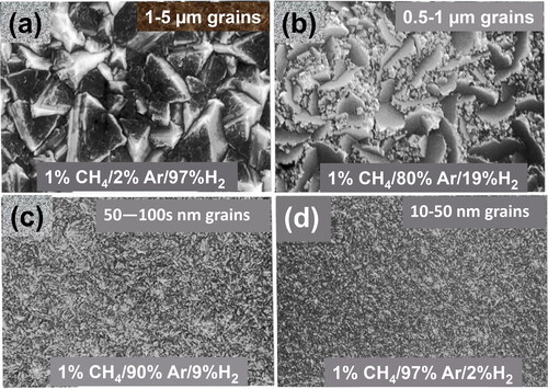
Figure 1. SEM micrographs showing grain sizes and surface morphology of PCD films grown with different CH4/Ar/H2 gas mixtures using the MPCVD process: (a) MCD film with rough surface morphology; (b) MCD film with less rough surface morphology than in (a); (c) and (d) NCD films with different grain size and surface morphology, depending on the increased Ar and decreased H2 percentage, as indicated in each figure above.
The H-induced etching of NCD grains, resulted in the effect that diamond grains that survived chemical etching were those that grew to larger size by statistical connection between nanograins, thus resulting in the observed MCD and NCD films [Citation1–8], thus, eliminating the feasibility of growing the transformational ultrananocrystalline diamond (UNCD) film, which is the focus of this review article. The name UNCD was coined by the developers of this film technology, as described below, and was based on the grain sizes of 3–5 nm, the smallest grain sizes of any PCD film grown today.
HFCVD growth of SCD, MCD and NCD films involve flowing mixtures of H2-rich (H2 (75-90%)/CH4 (3-2%) gases into an air evacuated chamber to ∼10−6 to 10−7 Torr, through an array of parallel tungsten filaments heated to ∼2000–2300 °C, via electrical current, inducing cracking of CH4 molecules upon impacting the hot filament surface, producing C and CHx (x = 1-3) molecules, which can induce growth of SCD and NCD to MCD films.
2. Fundamentals of ultrananocrystalline diamond (UNCD) films synthesis
This section focuses on reviewing the fundamental processes developed to grow the transformational unique UNCD films on different substrate materials, via microwave plasma chemical vapor deposition (MPCD) and hot filament chemical vapor deposition (HFCVD).
2.1. Synthesis of insulating UNCD films by MPCVD, using conventional seeding process of substrates and nanostructure and chemical characterization
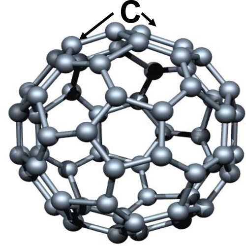
The first breakthrough, relevant to this review, in growing PCD films, with grains sizes < 10 nm, was produced by Gruen/Krauss et al. [Citation9], who demonstrated that Ar gas flowing through a circular oven heated to ∼900 °C, to evaporate C60 fullerene molecules [winner of a Nobel Prize by R.F. Curl Jr., Sir H. W. Kroto and R. E. Smalley [Citation10]), carried the C60 molecules () into an evacuated MPCVD chamber, where microwave power cracked the molecules, releasing C atoms that reacting chemically on substrates’ surfaces produced the growth of the UNCD films with 3–5 nm grain size [Citation9]. Subsequent research by Auciello/Krauss/Gruen et al. provided further evidence of the grow of UNCD films from fullerene molecules, revealing first evidence of the potential of UNCD films for new generation of electron field emission devices [Citation11].
Figure 2. Schematic of fullerene molecule showing the football-type geometry of the molecule with C atoms on the corners of pentagon-type cells.
The problem was that the C60 molecules-based film growth process was too expensive (1000 s of dollars for grams) to produce UNCD films at low cost for application to different technologies, plus the oven, producing the gas phase C60 fullerene molecules released substantial amount of carbon soot, an undesirable effect that contaminated the clean vacuum system to which the oven was connected.
The next breakthrough, to grow UNCD films at LOW COST, involved the discovery, led by Gruen/Krauss/Auciello et al. [Citation12], that replacing the H2 gas in the H2/CH4 gas mixture, used previously to grow from MCD to NCD films (see ) [Citation1–8], by Ar gas (the less expensive inert gas in the market today) to produce an Ar-rich (vol. 99%)/CH4 (vol. 1%) gas mixture in the MPCVD system, resulted in the growth of UNCD films with the same grain sizes of 3–5 nm size (see Ref. [Citation12], patent [Citation13] and reviews [Citation14, Citation15]), as produced with the C60 molecules-based film growth process.
Valuable information to understand the fundamental chemistry underlying the growth of UNCD films by MPCVD was provided by in situ/real-time optical emission spectroscopy (OES) imaging of the MPCVD plasma, generated with the Ar/CH4 gas mixture flow. The OES measurements showed a green plasma, with the color related to emission from excited C2 dimers, generated by the MPCVD process, from methane decomposition, via reactions (1) and (2) below:
(1)
(1)
(2)
(2)
The production of C2 dimers was originally proposed and demonstrated to play a critical role in the nucleation and growth of UNCD films (see reviews [Citation14, Citation15]). Initial calculations predicted that C2 dimers have low activation energy (∼6 kcal/mol) for insertion into the surface of substrates to induce the unique nucleation and growth of UNCD films. Subsequent modeling indicated that while the C2 population in the plasma is high, the population near the surface may be lower, and other hydrocarbon radicals (e.g. CH3, C2H2) may also contribute to the growth of UNCD films [Citation16]. However, the model relates to MPCVD growth of UNCD films, using a mixture of Ar∕CH4∕H2 gases, which does not produce the unique UNCD structure (with 3–5 nm grains) grown with the Ar/CH4 chemistry [Citation14, Citation15]. In addition, the model [Citation16] could not fully explain the low temperature growth of UNCD films, demonstrated for UNCD film growth at ∼400 °C. Regardless of the real mechanism, the distinctive characteristic of the UNCD film growth process is that the plasma contains very small quantities of hydrogen (about 1.5%).
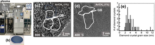
Auciello/Krauss/Gruen coined the name UNCD to designate the new transformational PCD film with grain size of 3–5 nm, as shown by HRTEM analysis (see and 3(d)). R&D demonstrated that UNCD films can be grown at substrate temperatures from 800 °C down to 400 °C, the latest being the lower temperature a PCD film grown today (). In addition, Auciello’s group was the first demonstrating the growth of UNCD films with excellent nanostructure and thickness uniformity, on up to 200 mm diameter substates (], using a top industrial MPCVD system (Innovative Plasma Systems IPLAS-GmbH, Germany-)), currently enabling commercialization of the UNCD coating technology for medical devise and implants by Original Biomedical Implant (OBI-USA (www.originalbiomedicalimplants.com) and OBI-México-Companies co-founded by Auciello and colleagues in 2013 and 2016, respectively).
Figure 3. (a) Industrial MPCVD system (IPLAS-GmbH, Germany) capable of growing UNCD films with excellent uniformity in thickness and nanostructure over 200 mm diameter substrates (b); HRTEM images of UNCD films grown by MPCVD on Si substrates at 800 °C (c) and 400 °C (d); (e) Diamond crystalline grain sizes in both UNCD films grown at 800 °C and 400 °C, showing the 3–5 nm grain size statistic defining the name UNCD.
Straightforward/fast characterization of the chemical nature of UNCD films, grown by MPCVD, has been and continuous to be performed using non-destructive Raman analysis, providing information on the chemical bonds of C atoms in the diamond crystalline grains and grain boundaries of UNCD and other PCD films, and graphite and graphene materials. (See details for Raman spectroscopy in a recent review [Citation17]). Raman spectroscopy confirmed the presence of sp3 diamond bonds of C atoms in the diamond crystalline lattice and sp2 C atoms bonds in the grain boundaries of UNCD and other PCD films. For Raman excitation produced by a LASER beam with visible wavelength (632 nm, 535 nm), the energy of the incident photons is much lower than the energy of the band gap for sp3 -bonded C, resulting in a much larger Raman scattering cross-section for sp2 – C bond than for sp3 - C bond due to the well-known resonant Raman effect [Citation17]. The Raman spectra observed from UNCD films are dominated by Raman peaks related to sp2-C bonds (the peak at 1560 cm−1 () corresponds to the G-mode Raman peak, arising from in-plane stretching modes of the sp2-C bond in UNCD grain boundaries [Citation14, Citation17]. The broad peak around the 1330 cm−1 (fingerprint of diamond) correspond to D-band type stretching of C-bonds in grain boundaries (see -Raman spectra from UNCD films grown with H2 (0-15%)). To see a well-defined diamond peak at 1332 cm−1 for UNCD films, UV laser needs to be used for the Raman analysis (see ). The peaks in the UV Raman spectra at 1550 cm−1 and 1560 cm−1 () are due to sp2– C atoms bonding in the grain boundaries [Citation14, Citation17, Citation18].
Figure 4. Raman spectra (obtained with a LASER beam wavelength in the visible range (a), showing the diamond peak at 1332 cm−1 only for NCD films grown with H2 flow ≥ 15%; (b) Raman spectra, obtained using a laser beam with UV wavelength, for the same polycrystalline diamond films analyzed with the visible laser (a), such that the UV laser enables seeing the diamond peak at 1332 cm−1, even for the UNCD film grown with H2 flow of 0% (Reprinted from Diamond and Related Materials, vol. 14, p. 86, 2005 (Figure 4) in [Citation27] with Permission from Elsevier Publisher).
![Figure 4. Raman spectra (obtained with a LASER beam wavelength in the visible range (a), showing the diamond peak at 1332 cm−1 only for NCD films grown with H2 flow ≥ 15%; (b) Raman spectra, obtained using a laser beam with UV wavelength, for the same polycrystalline diamond films analyzed with the visible laser (a), such that the UV laser enables seeing the diamond peak at 1332 cm−1, even for the UNCD film grown with H2 flow of 0% (Reprinted from Diamond and Related Materials, vol. 14, p. 86, 2005 (Figure 4) in [Citation27] with Permission from Elsevier Publisher).](/cms/asset/671f84d6-865a-4c57-9ecb-10582ffdc7c0/tfdi_a_2033606_f0004_b.jpg)
Confirmation that the dominant sp2-C bonds, observed by Raman in UNCD films, are not from an impurity graphite phase (i.e. parallel planes formed by hexagonal unit lattice with C atoms on the corner), but from dangling sp2-C bonds in grain boundaries, was provided by near edge X-ray absorption fine structure spectroscopy (NEXAFS) done on UNCD, MCD, and a crystal diamond gem. This technique is also defined as X-ray absorption near edge spectroscopy (XANES). Its sensitivity to the local atomic bond order in a material arises from the dipole-like electronic transitions from core atoms electronic states, which have well-defined orbital angular momenta, into empty electronic (e.g. antibonding) states. The symmetry of the final state can be determined, and thus the difference between sp2 and sp3 bonding can be readily observed in covalent, low-z materials like diamond. The NEXAFS spectra show the characteristic spectrum of crystalline diamond for UNCD, MCD and a diamond gem, which is completely different from the NEXAFS spectrum from a pure graphite film (see ) [Citation19]. In addition, NEXAFS analysis showed that UNCD films can be grown at substrate temperatures from 800 °C to 250 °C (see ).
Figure 5. (a) NEXAFS spectra from UNCD, MCD, and crystal diamond, showing that they are all identical and do not have graphite impurity, demonstrated by no graphite peak as shown in the graphite NEXAFS spectrum reference; (b) NEXAFS spectra from several UNCD films grown at different temperatures in the range 250–800 °C, showing that all UNCD films have the same chemistry and structure (Reprinted from Mat. Res. Soc. Proc., vol. 437, p. 211, 1996 (Figure 2) in [Citation19] with permission from Cambridge Publisher).
![Figure 5. (a) NEXAFS spectra from UNCD, MCD, and crystal diamond, showing that they are all identical and do not have graphite impurity, demonstrated by no graphite peak as shown in the graphite NEXAFS spectrum reference; (b) NEXAFS spectra from several UNCD films grown at different temperatures in the range 250–800 °C, showing that all UNCD films have the same chemistry and structure (Reprinted from Mat. Res. Soc. Proc., vol. 437, p. 211, 1996 (Figure 2) in [Citation19] with permission from Cambridge Publisher).](/cms/asset/d157a7c4-8100-4d40-889b-19bd42852363/tfdi_a_2033606_f0005_c.jpg)
A systematic comparison of structural, physical, chemical, mechanical, tribological, thermal, and electrical properties of MPCVD grown NCD and UNCD films is presented in , for the reader to have information that can help to make decisions on what type of PCD films could be used for specific application (MCD films properties are not included because they are two rough for the key applications discussed in this article).
Table 2. Comparison of the Properties of Highest Quality UNCD and NCD Films [Citation20].
The information on UNCD and NCD films synthesis by MPCVD, presented above, relates to films grown using the conventional chemical seeding process [Citation14, Citation15].
2.2. Synthesis of insulating UNCD films by MPCVD via bias enhanced nucleation (BEN)-bias enhanced growth (BEG) and chemical and nanostructure characterization
2.2.1. Background on MPCVD BEN-BEG of MCD and NCD films
The BEN process to nucleate polycrystalline diamond films was investigated and developed first for growing MCD and NCD films. The BEN process provides an alternative to the chemical diamond seeding process discussed in Section 2.1 above. The initial research focused on doing BEN followed by film growth without bias [Citation21, Citation22]. One initial research on BEN for growing MCD/NCD films [Citation22] revealed an enhanced nucleation density of diamond structure (1011 cm−2) on virgin Si surface vs. 107 cm−2 on Si surface seeded with diamond particles via mechanical polishing, The research described in [Citation21] revealed that PCD film growth with bias on resulted in very poor structural quality compared with films grown without bias after the BEN process. Analysis of diamond films, presented in [Citation14, Citation21], showed a formation of a SiC template layer on the Si surface before the diamond structure appeared on the film. Other research [Citation22], involved growing MCD/NCD films, using BEN (2–30 min), accelerating C+ and CHx+ ions, from plasmas produced with CH4/H2 gas mixtures (gas pressure of 20 mbar and 800 Watts microwave power), via substrates biases with voltages in the range –150 to –350 V. The 30 min BEN process was followed by conventional unbiased MPCVD growth process for about 30 min at 650–800 °C substrate temperatures. The research reported in [Citation22] showed that BEN-grown PCD films density reached a maximum for 80 eV bias energy, independent of the substrate temperature. This effect was interpreted as evidence that the BEN process involves C+ ions sub-plantation underneath the substrate surface, leading to SiC layer nucleation, inducing diamond film growth. Cross-section HRTEM imaging showed formation of Si pyramidal structures (see Figure 16 in [Citation22]) on top of which SiC interfacial layers were nucleated during the BEN process. However, no explanation was provided for the formation mechanism for Si pyramidal structures (see explanation below in the section describing the BEN-BEG of UNCD films). Raman analysis and x-ray diffraction presented in [Citation22] indicated that the MCD/NCD films/Si interface produced by BEN consists substantially of sp2 graphitic-type C bonds between the Si pyramidal structures, confirmed by an X-ray diffraction (XRD) (0002) peak of material between the Si pyramidal structures. The early work on BEN plus BEG processes, using CH4/H2 chemistries produced NCD (30–150 nm grains) not fully dense films (see Figure 15 in [Citation22]), relatively high surface roughness, high compressive stress, delamination of the film, and high content of non-diamond phase [Citation22]. Subsequent research revealed that electron emission from a substrate surface during BEN-of NCD film increased from zero to a stable value upon end of nucleation (Figure 1 in [Citation23]. The results reported in [Citation23] showed that BEN of NCD films, changed from ∼82 mins. for a CH4/H2 gas ratio of 3% to ∼10 mins. for a CH4/H2 gas ratio –15%. Also, the electron mission current change from zero to steady state changed from ∼70 mins, for a total gas pressure of 40 Torr, to ∼10 mins. for a total gas pressure of 55 Torr [Citation23]. Finally, the time for electron emission current stabilization, changed from ∼30 mins for 1000 Watts to ∼6 min for 1500 Watts. The data showed above demonstrated that the initial BEN process for MCD and NCD films, depends strongly on C+ and H+ ions contained in the plasma.
2.2.2. MPCVD BEN-BEG of UNCD films
Auciello’s group first performed R&D to develop a low-pressure bias-enhanced nucleation-bias enhanced growth (BEN-BEG) process to grow UNCD films. using the MPCVD-based BEN-BEG technique [Citation24], involving key steps, namely: 1) etching of the natural SiO2 layer on the surface of a Si (100) substrate, for 10 min, in a pure H-based plasma, with a substrate biased at – 350 V; 2) in situ BEN-BEG, using a H2 (93%)/CH4 (7%) gas mixture, based on the hypothesis that having substantial amount of H0 atoms and H+ ions in the plasma could help etch the impurity graphitic phase that in many cases growth concurrently with the diamond phase when growing NCD films [Citation22, Citation23]). The UNCD film was grown using a plasma produced by 2.2 kW microwave power at low 25 mbar pressure and applying −350 V bias on a substrate heated to 850 °C in a 2.45 GHz 6 in. IPLAS CYRANNUS MPCVD system () [Citation23]. Bias current density (Je) vs. time curves acquired under constant bias, during BEN-BEG of UNCD films, showed an abrupt increase of Je after an incubation period of about 5 min and saturation at ∼4.5 mA/cm2 at 15 min after the onset of the BEN process (). The abrupt increase and saturation of Je can be attributed to the rapid growth of diamond nuclei and subsequent full coverage of the substrate surface by the diamond grains, respectively (see detailed discussion in [Citation24]). The surface roughness of a 1 µm thick BEN-BEG UNCD film was ∼10 nm rms over a ∼10 µm2 area after Je reached steady state (), then reduced to ∼6 nm rms after 60 min film growth (), as revealed by AFM analysis ( [Citation24]. The BEN-BEG process described above yielded UNCD films with low stress, smooth surfaces (∼4–6 nm), high growth rates (∼1 µm/hr.) and uniform grain size (3–7 nm) throughout the whole film area on 100 mm diameter Si wafers () [Citation24].
Figure 6. (a) schematic of MPCVD components arrangement for performing BEN-BEG of UNCD films, showing plasma on negatively biased 100 mm diameter Si substrate; b) electron field emission current from biased substrate vs. BEN-BEG time for UNCD film growth, showing increase from 0 to stable 4. 5 mA/cm2 value (line curve) and UNCD film grain size reduction from ∼10 nm to 6 nm (dots) as the film reaches dense structure (f); (c) AFM image of UNCD film surface, showing 4–6 nm roughness, correlated with UNCD grain size; SEM images of UNCD film surface at 15 min (d), 30 min (e), and 60 min (f) of the BEN-BEG process; (f) SEM image of top surface morphology of dense BEN-BEG uniform UNCD film on 100 mm diameter Si surface, showing 1 µm thickness in 60 min growth (inset in (f)); (g) HRTEM image showing the characteristic grain sizes (3–5 nm) of UNCD films (reprinted from App. Phys. Lett., vol. 92, 133113, 2008 (Figure 3) in [Citation24] with permission from AIP Publisher).
![Figure 6. (a) schematic of MPCVD components arrangement for performing BEN-BEG of UNCD films, showing plasma on negatively biased 100 mm diameter Si substrate; b) electron field emission current from biased substrate vs. BEN-BEG time for UNCD film growth, showing increase from 0 to stable 4. 5 mA/cm2 value (line curve) and UNCD film grain size reduction from ∼10 nm to 6 nm (dots) as the film reaches dense structure (f); (c) AFM image of UNCD film surface, showing 4–6 nm roughness, correlated with UNCD grain size; SEM images of UNCD film surface at 15 min (d), 30 min (e), and 60 min (f) of the BEN-BEG process; (f) SEM image of top surface morphology of dense BEN-BEG uniform UNCD film on 100 mm diameter Si surface, showing 1 µm thickness in 60 min growth (inset in (f)); (g) HRTEM image showing the characteristic grain sizes (3–5 nm) of UNCD films (reprinted from App. Phys. Lett., vol. 92, 133113, 2008 (Figure 3) in [Citation24] with permission from AIP Publisher).](/cms/asset/ce4575e6-394c-40b6-8b79-b74d99f6a6ef/tfdi_a_2033606_f0006_b.jpg)
Raman analysis of MPCVD BEN-BEG UNCD films shows identical spectra as those shown in for UNCD films grown using the conventional NCD particles “seeding” process described in Section 2.1 above, so they will not be reproduced here.
HRTEM studies of the UNCD/Si interface for MPCVD BEN-BEG of UNCD film, on a Si substrate, revealed an etching effect on the Si surface, resulting in formation of triangular profile on the surface of the Si substrate, with a peak-to-valley roughness of about 15 nm and the surface of the triangular profile corresponding to the Si (111) planes, resulting from preferential sputtering of the (100) Si surface, due to higher sputtering of that crystal orientation, induced by bombardment of ions from the plasma, accelerated by the negative electric field applied to the substrate for the BEN-BEG process. SiC nucleation layers, observed on the tips of the triangular profiles, induced the growth of UNCD films. A summary on the mechanism for BEN-BEG of UNCD films on Si is presented in . Details of the BEN-BEG mechanism for growth of UNCD films can be found in Refs. [Citation24, Citation25].
Figure 7. (a) Cross-section HRTEM image of a BEN-BEG grown UNCD film on Si (100); (b) electron diffraction on the Si substrate, showing the diffraction points characteristic of Si; (c) electron diffraction on the UNCD film, showing the diffraction points characteristic of diamond; (d)) electron diffraction on the graphitic structured film area, showing the diffraction points characteristic of graphite; (e) schematic representing the mechanism of BEN-BEG growth for UNCD films; (f) SEM image of UNCD films grown by the BEN-BEG process on sharp Si tips for electron field emission devices; (g) UNCD films grown by BEN-BEG on many commercial Ti-alloy dental implants, showing the feasibility of using BEN-BEG as a much lower cost process to produce UNCD-coated implantable prostheses, eliminating the added cost process of chemical seeding described in Section 2.1. (Reprinted from J. App. Phys., vol. 105, 034311, 2009 (Figure 2 (b)) in [Citation25] with permission from AIP Publisher).
![Figure 7. (a) Cross-section HRTEM image of a BEN-BEG grown UNCD film on Si (100); (b) electron diffraction on the Si substrate, showing the diffraction points characteristic of Si; (c) electron diffraction on the UNCD film, showing the diffraction points characteristic of diamond; (d)) electron diffraction on the graphitic structured film area, showing the diffraction points characteristic of graphite; (e) schematic representing the mechanism of BEN-BEG growth for UNCD films; (f) SEM image of UNCD films grown by the BEN-BEG process on sharp Si tips for electron field emission devices; (g) UNCD films grown by BEN-BEG on many commercial Ti-alloy dental implants, showing the feasibility of using BEN-BEG as a much lower cost process to produce UNCD-coated implantable prostheses, eliminating the added cost process of chemical seeding described in Section 2.1. (Reprinted from J. App. Phys., vol. 105, 034311, 2009 (Figure 2 (b)) in [Citation25] with permission from AIP Publisher).](/cms/asset/dde7cc64-a927-4f86-a8ea-40418baa76a0/tfdi_a_2033606_f0007_c.jpg)
2.3. MPCVD Synthesis of electrically conductive nitrogen grain Boundaries-Incorporated N-UNCD films and nanostructure, chemical and electrical conductivity characterization
The first pioneering synthesis of electrically conductive N-UNCD films was done by Auciello et al., when investigating the possibility of producing corrosion-resistant/electrically conductive diamond films for electron field emission devices (e.g. field emission displays) [Citation26]. N atoms-grain boundary incorporated UNCD (named N-UNCD) films were grown using first the MPCVD BEN-BEG process on high conductivity Si substrates, based on the hypothesis that N+ ions, in the MPCVD’s plasma, could be accelerated towards negatively biased substrates to implant N atoms in the UNCD films, to provide electrons for electrical conduction through grain boundaries. The initial R&D [Citation26–28] showed that when N2 gas is inserted in the original Ar/CH4 gas mixture, used to grow insulating UNCD films, the MPCVD created plasma contains C2 dimers and CN radicals, due to C-N atoms chemical reaction in the gas phase, such that the CN content increases substantially as N2 gas is added to the Ar/CH4 gas mixture. Small additions of N2 (1%–5%), resulted in nanostructure similar to the UNCD films (3–7 nm grains and ∼0.4 nm grain boundaries) (see and 8 (b), (e), respectively)), while addition of N2 (20%) to the Ar/CH4 gas mixture produced the N-UNCD films with grains of 7–16 nm dimensions and grain boundaries with 1–2 nm width (see and (f) [Citation28, Citation29].
Figure 8. HRTEM images of N-UNCD films grown with Ar/CH4 gas mixture with N2 (0%) (a)-low resolution/(d) high-resolution; N2 (5%) (b)-low resolution/(e) high-resolution; N2 (20%) (c)-low resolution/(f) high-resolution (this show the initial characterization of N-UNCD films revealing the enlargement of grains and grain boundaries with respect to UNCD films revealed in the original first demonstration of MPCVD-grown N-UNCD films (Reprinted from App. Phys. Lett., vol. 81 (12), p. 2235, 2002 (Figure 1) in [Citation29] with permission from AIP Publisher).
![Figure 8. HRTEM images of N-UNCD films grown with Ar/CH4 gas mixture with N2 (0%) (a)-low resolution/(d) high-resolution; N2 (5%) (b)-low resolution/(e) high-resolution; N2 (20%) (c)-low resolution/(f) high-resolution (this show the initial characterization of N-UNCD films revealing the enlargement of grains and grain boundaries with respect to UNCD films revealed in the original first demonstration of MPCVD-grown N-UNCD films (Reprinted from App. Phys. Lett., vol. 81 (12), p. 2235, 2002 (Figure 1) in [Citation29] with permission from AIP Publisher).](/cms/asset/9bce5a2b-f969-4628-952b-690f406edf2a/tfdi_a_2033606_f0008_b.jpg)
Raman spectra, obtained with a visible laser beam (632 nm), from analysis of N-UNCD films grown with N2 gas contents in the range 0-20%, are shown in . The spectra reveal the characteristic D-band peak at 1340 cm−1 and G-band peak at 1556 cm−1, correlating with sp2-binding of C atoms, and a shallow shoulder at 1140 cm−1, attributed to nanocrystalline diamond [Citation28, Citation29]. The Raman spectra reveal increasing G-band peak intensity over the D-band peak intensity vs. increase of N atoms content in the plasma, including a slight peak shift to higher wavenumber, correlating with a slight change in sp2-C atoms bonds in grain boundaries. Complementary chemical analysis was necessary to support molecular dynamic simulations [Citation30] indicating that N atoms bonding to open sp2-C atoms, in grain boundaries of N-UNCD films, contributed to release electrons, providing high electrical conductivity through grain boundaries. The complementary analysis was done via mall-spot HRTEM-based EELS, revealing C atoms bonding structure in grains and grain boundaries in N-UNCD films grown with an increasing amount of nitrogen in the plasma [Citation29]. EELS spectra, taken on grain boundaries of N-UNCD films, shown in , reveals that the π* peak, at ∼285 eV, increases slightly when N2 gas, during N-UNCD film growth, increases from 0% to 20%, contributing N atoms insertion into the N-UNCD films’ grain boundaries. The σ* peak at ∼290 eV, associated with diamond sp3-C atoms bonds in the grains, is unchanged. The relative intensities of the sp2 vs. sp3 peaks in the EELS spectra in indicate that the number of sp2-C atoms bonds increase slightly within the grain boundaries of N-UNCD films, with N2 gas flow, inducing No atoms and N+ ions concentrations increase in the MPCVD plasma process [Citation29]. The Raman and EELS spectra shown in and 9 (b), respectively, correlates with the resulting N atoms concentration and electrical conductivity increase in N-UNCD’s grain boundaries ().
Figure 9. (a) Spectra from Raman analysis of N-UNCD films grown with Ar/CH4 gas flux with N2 gas added from 0% to 20% for five different N-UNCD films; (b) HRTEM-EELS analysis in grain boundaries of the same N-UNCD films, for which Raman spectra are shown in (a) (Reprinted from App. Phys. Lett., vol. 81 (12), p. 2235, 2002 (Figure 2) in [Citation29] with permission from AIP Publisher); (c) Total N atoms content (left axis), determined via secondary ion mass spectrometry (SIMS) depth profile analysis of N-UNCD films, and room-temperature electrical conductivity (right axis) vs. percentage of N2 gas flow during film growth, inducing No atoms and N+ ions concentrations increase in the MPCVD plasma process.
![Figure 9. (a) Spectra from Raman analysis of N-UNCD films grown with Ar/CH4 gas flux with N2 gas added from 0% to 20% for five different N-UNCD films; (b) HRTEM-EELS analysis in grain boundaries of the same N-UNCD films, for which Raman spectra are shown in (a) (Reprinted from App. Phys. Lett., vol. 81 (12), p. 2235, 2002 (Figure 2) in [Citation29] with permission from AIP Publisher); (c) Total N atoms content (left axis), determined via secondary ion mass spectrometry (SIMS) depth profile analysis of N-UNCD films, and room-temperature electrical conductivity (right axis) vs. percentage of N2 gas flow during film growth, inducing No atoms and N+ ions concentrations increase in the MPCVD plasma process.](/cms/asset/43260753-1385-4a52-b427-c839b4d0f9e4/tfdi_a_2033606_f0009_b.jpg)
N-UNCD films grown by another independent group, using the MPCVD process, with 20% N2 gas concentration, revealed relatively higher values that those grown with 10% N2 films, supporting the data shown in , initially obtained by Auciello et al. [Citation28, Citation29]. The estimated values of N atoms concentration, in the N-UNCD films, of about 1020 cm−3, can explain the high conductivity of these films and suggests that the N-UNCD films transport can reach the high end of the diffusive regime enabling band-like conduction.
A key analysis of N-UNCD films was done using atomic scale resolution “Atom-Probe Analysis”, to determine if N atoms were inserted in the grain boundaries. N-UNCD films with the hypothesized N atoms inserted in the grain boundaries, were grown on atomically sharp tips. The tips were inserted in holder in an ultra-high vacuum system, where they were biased with a high positive potential with respect to a detector at ground potential, while picosecond laser pulses, impinging on the specimen’s microtip along the axis, triggered electric field-induced evaporation of ions from the surface of the N-UNCD-coated tip. The ions were accelerated along diverging electric field lines on the tips to project a highly magnified image of the microtip’s surface onto a position-sensitive time-of-flight detector. The time-of-flight of the ions was used to identify their mass-to-charge-state ratio and hence their chemical identities (see Figures 2, 3, and 4 in [Citation31], for detailed explanation of the technique). 3 D-tomographic atom-probe tomography reconstructions of nano-diamonds provided information about the N and C atoms in the grain boundaries of N-UNCD films (see Figure 6 in [Citation31], showing maps of single atoms distribution. These measurements provided key information confirming the presence of N atoms in the N-UNCD grain boundaries, supporting the modeling [Citation30] and electrical measurements [Citation27] indicating that the N atoms reacting with dangling C atoms bonds and releasing electrons for electrical conduction through the grain boundaries.
2.4. UNCD films synthesis by HFCVD, using conventional seeding process and Bias Enhanced Nucleation-Bias Enhanced Growth (BEN-BEG) and nanostructure and chemical characterization
Most films grown by HFCVD exhibited grain size in the NCD (> 10 nm) range, and no systematic analysis on the uniformity of the nanostructure and film thickness has been reported. Auciello’s group performed the first series of systematic studies focused on investigating HFCVD-based growth process to produce UNCD films (3–5 nm grains) [Citation32, Citation33] with high uniformity in thickness and surface roughness, on 100 mm-diameter Si substrates (). The growth of polycrystalline diamond films by the HFCVD process, reviewed in this section, was done on tungsten (W) template layers grown on SiO2/Si substrates, since prior research by Auciello et al. demonstrated that W surface induce the highest nucleation density for UNCD film growth (see review in [Citation14]). Different gas flow chemistries were investigated to determine the conditions to grow polycrystalline diamond films from MCD (∼1μm) to NCD (≥10 nm grain) to UNCD films for applications to new generations of micro/nano-electronics and MEMS/NEMS devices. The studies related to HFCVD growth of MCD to UNCD films involved systematic analysis of films, using complementary High-Resolution Transmission Electron Microscopy (HRTEM) to determine nanostructure, X-Ray Diffraction (XRD) and Atomic Force Microscope (AFM) to determine grain size and surface roughness, respectively, Scanning Electron Microscopy (SEM) and Raman analysis, visible (532 nm laser wavelength) and far UV (244 nm laser wavelength), were used to characterize the films surface morphologies and C atoms chemical bonds, respectively.
Figure 10. (a) Schematic of HFCVD system used for investigating and developing the UNCD film growth process. b) picture of HFCVD system growing a UNCD film on a 100 mm diameter Si wafer with the surface nanocrystalline diamond substrate “Seeded” by the chemical process described in Section 2.1; (c) picture of UNCD film grown during the process shown in (b); (d) picture of the HFCVD system during grown of a UNCD film on a Si wafer, using the BEN-BEG process described above (a plasma (white area) is established on the substrate surface; (e) Modeling showing the electric field distribution across the substrate between the positively biased filaments and the negatively biased substrate, to attract C+, CHx+, H+, and Ar+ ions formed in the plasma produced by the filament-substrate electric field; f) picture of the HFCVD system during selective BEN-BEG growth of UNCD films on tungsten (W) micron scale lines grown on a Si wafer to demonstrate BEN-BEG-induced selective growth of UNCD films on Si wafers for MEMS/NEMS and microelectronic device fabrication; (g) BEN-BEG selectively grown UNCD film on W lines on a 100 mm Si wafer (Reprinted from Diamond and Related Materials, vol. 78, p. 1, 2017 (Figure 1) in [Citation33] with permission from Elsevier Publisher).
![Figure 10. (a) Schematic of HFCVD system used for investigating and developing the UNCD film growth process. b) picture of HFCVD system growing a UNCD film on a 100 mm diameter Si wafer with the surface nanocrystalline diamond substrate “Seeded” by the chemical process described in Section 2.1; (c) picture of UNCD film grown during the process shown in (b); (d) picture of the HFCVD system during grown of a UNCD film on a Si wafer, using the BEN-BEG process described above (a plasma (white area) is established on the substrate surface; (e) Modeling showing the electric field distribution across the substrate between the positively biased filaments and the negatively biased substrate, to attract C+, CHx+, H+, and Ar+ ions formed in the plasma produced by the filament-substrate electric field; f) picture of the HFCVD system during selective BEN-BEG growth of UNCD films on tungsten (W) micron scale lines grown on a Si wafer to demonstrate BEN-BEG-induced selective growth of UNCD films on Si wafers for MEMS/NEMS and microelectronic device fabrication; (g) BEN-BEG selectively grown UNCD film on W lines on a 100 mm Si wafer (Reprinted from Diamond and Related Materials, vol. 78, p. 1, 2017 (Figure 1) in [Citation33] with permission from Elsevier Publisher).](/cms/asset/896557c3-d0e5-4420-99b1-1653bf5e09ac/tfdi_a_2033606_f0010_c.jpg)
2.4.1. HFCVD-based UNCD film growth via conventional chemical seeding process
The HFCVD film growth process [Citation32, Citation33] involves an array of W filaments (ø = 0.25 mm, length ∼14.2 cm) held on a Molybdenum (Mo) frame, in an optimized geometry, positioned 3 cm above the substrate holder (). The substrates were located on a metal disk, rotated during film growth to induce film thickness uniformity on up to 100 mm diameter substrates (). The filaments were heated to 2200 °C by passing AC current. The gases flows were: (a) H2 (200 sccm)/CH4 (3 sccm) producing MCD films (); (b)/Ar (50 sccm)/H2 (50 sccm)/CH4 (2 sccm) producing medium Grain size NCD films (); (c) Ar (70 sccm)/H2 (30 sccm)/CH4 (2 sccm) producing small grains NCD films (); (d) Ar (90 sccm)/(10 sccm)/CH4 (2 sccm) producing UNCD films, as shown by SEM top and cross-section (insert) SEM images ( and HRTEM image showing the UNCD grain size (3–5 nm) and electron diffraction (insert) showing the diamond lattice (). The gas mixture flow is set-up to produce uniform pressure of 10 Torr in the film growth chamber. The geometry of the HFCVD, and specifically the filament arrays, induces cracking of H2, CH4 gas molecules impacting on the hot filaments’ surface (), resulting in C, CHx (x = 1, 2, 3) molecules, and H atoms, which interacting with the Ar atoms, on the substrate surface () induce the growth of MCD to UNCD uniform films, depending on the H2/CH4 gas flow ratios, on up to 100 mm diameter substrates () used until now.
Figure 11. SEM images of PCD films grown by the HFCVD process on Si substrates, with chemical NCD particles seeding process, using the gas flows indicated on each figure: (a) MCD film; (b) NCD film with medium size grains; (c) NCD film with small size grains; (d) UNCD film with the characteristic 3–5 nm grain size and similar surface roughness (insert cross-section SEM image); (e) HRTEM image of the UNCD film which SEM image is shown in (d) (The insert shows the electron diffraction pattern confirming that the UNC D grains are made of diamond) (Reprinted from Thin Solid Films, vol. 603, p. 62, 2016 [Citation32] with permission from Elsevier Publisher).
![Figure 11. SEM images of PCD films grown by the HFCVD process on Si substrates, with chemical NCD particles seeding process, using the gas flows indicated on each figure: (a) MCD film; (b) NCD film with medium size grains; (c) NCD film with small size grains; (d) UNCD film with the characteristic 3–5 nm grain size and similar surface roughness (insert cross-section SEM image); (e) HRTEM image of the UNCD film which SEM image is shown in (d) (The insert shows the electron diffraction pattern confirming that the UNC D grains are made of diamond) (Reprinted from Thin Solid Films, vol. 603, p. 62, 2016 [Citation32] with permission from Elsevier Publisher).](/cms/asset/b5621b60-ff9d-4043-ad83-57ddec638eff/tfdi_a_2033606_f0011_c.jpg)
Raman analysis of the UNCD films, produced by the HFCVD process, show identical Raman spectra as those shown for UNCD films produced by the MPCVD process ().
In relation to reviewing growth of UNCD films by the HFCVD technique, it is relevant to review the conditions and parameters involved in growing PCD films (MCD, NCD, and UNCD). in this sense, summarizes key publications on HFCVD growth of PCD (MCD, NCD, UNCD) films by different groups worldwide.
Table 3. Film growth parameters, diamond film structures and characterization techniques used to characterize the PCD films grown by HFCVD, as reported in the literature.
2.4.2. HFCVD-based UNCD film growth via BEN-BEG process
Research was performed from 2000 to 2017 by different groups focused on investigating the HFCVD-based BEN-BEG process to grow PCD films. The research resulted in growth of MCD (≥ 1 µm grains) to NCD (∼20 100 s nm grains) films. References in from Ref. [Citation32] shows that most of the research was focused on HFCVD BEN-BEG of PCD films on Si++ substrates, mostly of small areas (10-50 mm diameter), except for the research reported in [Citation32], describing an attempt to produce HFCVD/BEN-BEG-based NCD films on a 100 mm diameter Si substrate but were not able to cover the substrate with uniform film all the way to the edge [Citation34].
Based on the information presented above, Auciello’s group performed the first systematic studies to develop a HFCVD BEN-BEG process to grow uniform UNCD films on 100 mm diameter Si substrates, as an intermediate stage to scale to ≥ 200 mm diameter wafers. Si wafers (100 mm diameter) were coated with 40 nm thick W layers, to provide high electrical conductivity surfaces and high density UNCD films growth, as demonstrated for MPCVD growth of UNCD films [see review in Ref. [Citation14])] grown on W-coated Si substrates, via formation of a WC-nucleation layer, inducing the UNCD film growth [Citation14]. The research cited in [Citation32, Citation33] showed that the HFCVD/BEN-BEG process can be applied to other substrates with different electrical conductivity. The importance of understanding the UNCD HFCVD BEN-BEG growth process on large area substrates, other than Si, specifically on carbide surface layers-forming materials, such as W, Ti, Mo, and more, is because it opens new technological applications of UNCD-coated products at lower cost than using the chemical seeding process, currently used in commercial production of UNCD-coated industrial mechanical pump seals and bearings [Citation42] by Advanced Diamond Technologies (company co-founded by Auciello and colleagues). In addition, HFCVD BEN-BEG of uniform UNCD films over larger areas will enable selective/directional growth of UNCD films on patterned W structured layers for fabrication of devices on large area wafers using in the semiconductor industry [Citation33].
The HFCVD system used for the research on HFCVD BEN-BEG of UNCD films is shown in . shows a picture of the HFCVD in operation revealing the plasma produced on top of the substrate surface, from where the + charged C+, CHx+, H+ and Ar+ ions are accelerated towards the negatively (-) biased substrate, inducing sub-implantation of C atoms under the surface as the UNCD film BEN-BEG process. shows schematic of the model developed to calculate the electric fields inducing the BEN-BEG process. shows a picture of an HFCVD BEN-BEG process growing UNCD films selectively on micron/nanoscale W layers-based diamond form structures, while shows a diamond shaped W structure coated with UNCD films. The selective BEN-BEG process [Citation33] will enable development of micro-/nano-electronic and MEMS/NEMS devices.
The studies on HFCVD BEN-BEG of UNCD films benefited from the use of complementary techniques to characterize the UNCD films growth process across 100 mm diameter Si substrates.
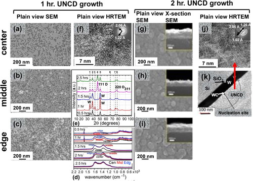
A critical parameter related to HFCVD BEN-BEG UNCD film growth process is the time taken for nucleation of initial UNCD grains on the substrate surface, during the BEN step, followed by the BEG process that results in the growth of continuous UNCD films. In the systematic studies reviewed here the HFCVD BEN-BEG time was changed in the range 0.5–2.5 hrs. adding 2 hrs. of film growth time without bias for each film. The filaments were heated to 2300 °C during films’ growth. A mixture of gases with ratio of H2 (49 sccm)/CH4 (2 sccm)/Ar (49 sccm) was flown into the air evacuated (to 3x10⁻⁶ Torr) HFCVD chamber. The substrate was heated to 550 °C via a filament-based heater. Further experimental details can be found in Ref. [Citation33]. The BEN-BEG process was performed applying a voltage of ∼–220 Volts on the substrate, to keep a constant electrical current of 1.5 A through the plasma. SEM imaging showed that the initial surface morphology of the UNCD coating exhibited relatively smaller number of grains in the center and middle areas (and (b)), respectively, than in the edge (), where the electric fields were stronger. The surface morphology correlated with the information presented in the Raman spectra (-0.5 hr.) showing very small similar peaks intensities on all areas) and XRD spectra showing an almost no noticeable peak of (111) diamond at ∼2θ = 48˚ (-0.5 hrs. spectra). shows a HRTEM image of the Si wafer center area, for 0.5 hrs. UNCD film growth, revealing very little evidence of UNCD coating, correlating with the Raman (-0.5 hrs.) and XRD (-0.5 hrs.) Spectra. The SEM images shown in , h, and I) reveal the surface topography of the dense UNCD film in the Center, Middle, and Edge areas, after 2 hrs. growth, correlating with the Raman spectra of -2 hrs. film growth, showing uniform Raman peaks of UNCD films in all three areas, and XRD spectrum (-2 hrs. film growth, showing the main (111) smaller (220) and (311) diamond lattice peaks, all confirming the excellent UNCD film growth by HFCVD BEN-BEG process. The surface chemistry of the UNCD films was characterized by X-ray Photoelectron Spectroscopy (XPS) (see Ref. [Citation33] for detailed description of the XPS analysis. Details of all the characterization systems and parameters used for the analyses can be found in [Citation33].
Figure 12. SEM images of UNCD films grown by the HFCVD BEN-BEG process on a 100 mm diameter Si wafer, using the gas flows described in the text above . SEM images of Center (a), Middle (b), and Edge (c) areas of the Si wafer after initial 0.5 hrs. of BEN process, showing very small growth, confirmed by the Raman spectra shown in (d) for the 0.5 hrs. time; (e) XRD spectra from UNCD films grown on the Si wafer showing mainly the W peaks, corresponding to the W layer on the Si wafer, and practically no (111) diamond peak, correlated with the Raman spectra in (d) and practically no evidence of UNCD films in the SEM (a), (b), and (c) images and the HRTEM image (f); SEM images of Center (g), Middle (h), and Edge (f) areas of the Si wafer after full grown UNCD film, correlating with the Raman spectra at 2 hrs. growth (d) and the strong (111) and small (220) and (311) diamond peaks in the XRD spectrum taken after 2 hrs. growth (e), all revealing the dense UNCD film grown in 2 hrs.; j) HRTEM image of the 2 hrs. grown UNCD film area revealed on the nucleated WC area shown in k).
The R&D on HFCVD BEN-BEG growth of UNCD films on W template layers on Si was used to demonstrate that UNCD films can be grown selectively on micron-size patterned W layers to eventually develop a BEN-BEG process to produce, in the future, electronic device-based structures. In summary, the HFCVD BEN-BEG provides a transformational industrial-type growth process to produce UNCD coatings on large area substrates at low cost for development of new generations of UNCD-coated industrial, high-tech, and external and implantable medical devices and prostheses, as briefly reviewed in the next section.
shows key information on parameters used by several groups worldwide performing R&D to grow MCD to UNCD films using the HFCVD BEN-BEG process. The readers can get further detailed information from the references cited in .
Table 4. Information on parameters used for HFCVD BEN-BEG synthesis of NCD to UNCD films by independent groups worldwide (Reprinted from Diamond and Related Materials, vol. 78, p. 1, 2017 in [Citation33] with permission from Elsevier Publisher).
3. Brief review of key products based on multifunctional UNCD coatings
3.1. UNCD-Coated industrial and high-tech products in the worldwide market
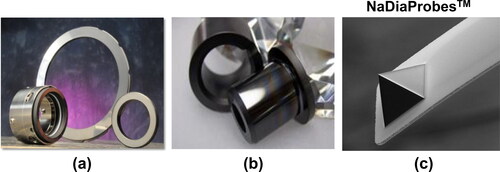
The chemistry and atoms bonding configuration on UNCD coating surfaces resulted in unique nanotribological properties (lowest coefficient of friction (0.02-0.04) compared to any other PCD films, and outstanding resistance to mechanical wear), both of which enabled new generations of mechanical pump seals () and bearings (), and atomic force microscope (AFM) tips (NaDiaProbesTM) (), providing practically wear-free/high resolution AFM nanolithography and imaging capabilities. All these products are currently produced via growth of UNCD coating and marketed worldwide by Advanced Diamond Technologies (only company marketing products based on UNCD coatings, co-founded by Auciello et al. in 2003 [Citation42], profitable in 2014, sold for profit to a large company in 2019).
Figure 13. (a) UNCD-coated commercial SiC mechanical pump seals (∼U$S 600 million market) providing 0.02–0.04 coefficient of friction (saving up to 20% in cost of energy to make the pump work) and negligible wear for years; (b) biocompatible/anti-fouling UNCD-coated bearings (∼U$S 1.5 billion market) for mechanical pumps used in producing pharmaceutical drugs by Merk Millipore; (c) UNCD-based AFM tips (∼U$S 200 million market), provide orders of magnitude longer life than Si, metal, and other tips, since UNCD AFM tips practically do not wear.
3.2. RF-MEMS switches with superior UNCD dielectric layers for MEMS phase shifters
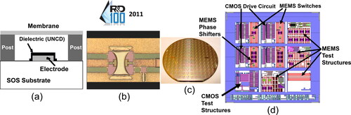
R&D performed by Auciello’s group demonstrated that UNCD films exhibit excellent dielectric properties, enabling a new generation of dielectric layers for RF MEMS switches [Citation50] (). The UNCD dielectric layer provides, for the first time, the capability for RF MEMS switches without failure as it occurred in prior switch technologies involving dielectric layers made of SiO2 or Si2N3, which failed due to electrical charging (∼80 µsec) of the oxides and nitrides and long discharging times (∼hundreds of seconds), leading to sticking of the movable switch membrane to the dielectric layer on top of the bottom electrode, thus failure [Citation50]. RF-MEMS switches with UNCD dielectric layers, exhibit fast charging and discharging, both in ∼80 µsec, due to the large grain boundary network of the UNCD layer, thus eliminating the electrical charging failure [Citation50].
Figure 14. (a) Schematic and (b) SEM image of RF-MEMS switch with UNCD dielectric layer; (c) 200 mm diameter Si wafer with integrated RF-MEMS switch with UNCD dielectric layer and MEMS phase shifters and CMOS devices; (d) picture of integrated MEMS Phase Shifters with UNCD-based MEMS RF-switches and CMOS driving devices.
3.3. Integrated Piezoelectric/UNCD films in MEMS cantilevers enabling transformational biosensors and power generation for implantable medical devices
3.3.1. Biosensors and power generation for implantable medical devices
The outstanding mechanical (highest hardness) and tribological (lowest coefficient of friction and hydrophobicity) properties of UNCD films enable their application to produce a new generation of transformational microelectromechanical/nanoelectromechanical systems (MEMS/NEMS) devices [Citation51, Citation52], including the first demonstrated UNCD/piezoelectric oxide films integration to produce piezoelectrically actuated UNCD-based MEMS/NEMS biosensors and energy generation implantable devices [Citation52]. A brief description of the process for producing integrated UNCD/piezoelectric oxide films-based MEMS/NEMS technology is presented below:
(i) UNCD films are grown on SiO2 layers on Si, followed by growth of SiO2 and masking layers on the UNCD films and subsequent lithography plus reactive ion etching (RIE) to define UNCD cantilever structures (), followed by growth of Pt/PbZrxTi1-xO3 (PZT)/Pt layers on the UNCD films (). shows a cross-section SEM image of PZT/Pt films grown on a 40 nm TiAl layer (exhibiting the lowest energy of oxide formation), used as diffusion barrier to inhibit O atoms, used to grow the PZT films at ∼500–600 °C, of reaching the UNCD film, which would be chemically etched if exposed to O atoms at high temperature [Citation51, Citation52].
Figure 15. (a) Schematic of UNCD-based MEMS/NEMS cantilevers produced by lithography plus RIE process; (b) schematic of integrated Pt/PZT/Pt/UNCD cantilevers released by HF acid etching of underlying SiO2 layer; c) cross-section SEM image of integrated PZT/Pt/UNCD films with a 40 nm TiAl layer at the Pt/UNCD interface. to inhibit O atoms, diffused through the Pt layer, during growth of the PZT films in an oxygen atmosphere, to reach the UNCD film, which would result in chemical etching of the UNCD material; (d) polarization vs electric field for the PZT layer, which induce integrated Pt/PZT/Pt/TiAl/UNCD films-based cantilever motion to detect damaging biomolecules when reacting with conjugated biomolecules grown on the UNCD cantilever surface, changing the vibration (e and f); (g) Schematic of integrated Pt/PZT/Pt/TiAl/UNCD MEMS cantilever actuated by vibrating heart cells from mice (see associated SEM images), producing electrical current (power) to provide energy to implantable medical devices, such as defibrillator/pacemakers.
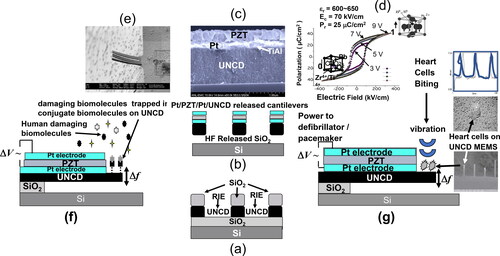
(ii) Figure 15 (d) shows the excellent polarization vs. electric field (applied between the Pt electrode layers encapsulating the PZT film) polarization loop, which induce the UNCD cantilever motion when excited by the electric field (for biosensor operation) (, or energy generation when the cantilever is excited by mechanical motion ().
(iii) Figure 15 (e) shows an SEM image of an array of integrated Pt/PZT/Pt/UNCD cantilevers that were excited by 3 V to billions of cycles without failure, demonstrating the biosensor () operation
(iv) Figure 15 (g)) shows a schematic of an integrated Pt/PZT/Pt/UNCD cantilever, mechanically actuated by biting heart cells of mice, grown very efficiently on the excellent biocompatible UNCD layer surface, resulting if electrical current (power) generation to enable powering a new generation of defibrillator/pacemakers, eliminating the need for batteries.
The integrated Piezoelectric/UNCD films-based MEMS/NEMS technology may enable new transformational external and implantable biosensors and energy generation devices. However, it is critical to replace the piezoelectric PZT film with another that does not contain lead (Pb) and is biocompatible. In this sense, a potential biocompatible piezoelectric material that can be used to replace the PZT film is BiFeO3 (BFO), which is being investigated for application as a piezoelectric and photovoltaic material, but no evidence of biocompatibility is found in the literature.
Preliminary R&D recently performed by Auciello’s group [Citation52, Citation53] demonstrated that BiFeO3 (BFO) and SrTiO3 (STO) films integrated into novel BFO/STO)/BFO nanolaminates (BSB-NLs), featuring nanometer-scale thickness of BFO and STO layers can be tailored, via introduction of STO layer in between two BFO layers, such that an optimized STO layer thickness can produce the highest piezoresponse value and lowest leakage current demonstrate today for BFO-based piezoelectric films, for integration into new piezoelectrically actuated biosensors and power generation devices, with these nanolaminates providing biocompatible piezoelectrically-based materials, since both BFO and STO layers are formed by potential biocompatible materials (Bi is inserted in the gastrointestinal relief medicament named “Pectobismol”. Fe is in the human biological environment, strontium is also biocompatible, and oxygen is a component of air bread by humans). A detailed description of the R&D being performed on BSB-NLs can be found in [Citation52, Citation53].
3.4. Key High-Tech devices based on electrically conductive N-UNCD and Boron-Doped B-UNCD films
3.4.1. N-UNCD-coated anodes for Li-Ion batteries
The N-UNCD film technology described in Section 2.3 and detailed reviews [Citation14, Citation26–29] and patent [Citation28], enables a new generation of metal electrodes for new generation of implantable neural stimulation electrodes and, very importantly, a new generation of Li-ion batteries (LIBs) with ≥ 10x longer stable energy capacity vs. charge/discharge (), and safer than current LIBs, based on the extremely corrosion resistant N-UNCD coating of anodes () and -right [Citation54, Citation55], which eliminate destructive Li-induced corrosion of current commercial natural graphite (NG)/copper (Cu) anodes (-left XRD spectrum).
Figure 16. (a) Schematic of current commercial NG/Cu anode in LIBs (top) and cross-section HRTEM (middle) and LRTEM (bottom) images of UNCD-coated commercial NG/Cu anode; (b) Energy Capacity vs charge/discharge cycles, showing the stable superior performance of the N-UNCD-coated NG/Cu anode (red curve); (c) XRD analysis of the commercial NG/Cu anode (left spectrum), used in obtaining the black energy capacity curve in (b), shows the formation of LiC6, LiC12, and LiC24, resulting in chemical degradation of the NG layer and substantial reduction in energy capacity; on the other hand the XRD curve on the left side shows that the integrated N-UNCD/NG layer does not exhibit any chemical degradation, which correlates with the stable energy capacity (red curve in (b)).
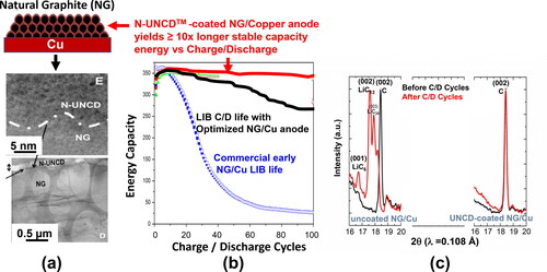
The initial results from R&D on N-UNCD-coated NG/Cu anodes for LIBS indicate that there is a great potential for Li-corrosion resistant N-UNCD coatings to make a major contribution to develop a new generation of LIBs with order of magnitude longer energy life before charging and safer than current LIBs.
3.4.2. B-UNCD-coated metal electrodes for water purification systems
Alternatively, to electrical conduction by nitrogen incorporation into the grain boundaries, highly conductive UNCD films have been achieved by true semiconductor doping, via inserting Boron (B) atoms replacing C atoms in the diamond lattice and providing electrons to the conduction band. MPCVD plasma-induced film growth process, using a CH4/H2/trimethyl borate (B(OCH3)3 (TMB) gas mixture inserts up to ∼1020 cm−3 B atoms concentration, replacing C atoms in the diamond lattice in grains, inducing metallic-type electrical conductivity [Citation56]. HFCVD was also used by ADT [Citation42] to grow B-UNCD coatings on metal electrodes for water purification systems. However, MPCVD and HFCVD growth process for producing B-UNCD films contaminates the systems, inhibiting their use for growing any other UNCD films. This problem was solved recently by Auciellos’ group who developed a new process involving growing UNCD films on metal or other substrates by MPCVD and HFCVD, followed by a Spin-on-Dopant (SOD) B-containing film (∼200 nm thick), dispersed on the UNCD films’ surface via a spinning, and subsequent rapid thermal annealing (RTA) in a dedicated separate system, at 800˚ –1000 °C, to determine the optimum temperature for optimum diffusion depth of B atoms inside the UNCD films, to achieve highest electrical conductivity (a detailed description of the UNCD film growth plus external B doping can be found in Ref. [Citation57]. Metal electrodes are currently coated with totally water corrosion resistant B-UNCD films, produced at low cost, in large area HFCVD systems, growing extremely uniform films on up to 50 x 50 cm2 area. The B-UNCD-coated electrodes are currently used in prototype water purifications systems [Citation42], where purification is done very efficiently via passing electrical current between electrodes and creating ozone (O3) molecules, which kill all viruses, bacteria, and any other pathogen in the water.
3.4.3. N-UNCD-coated cathodes for electric Field-Induced electron emission for High-Tech systems
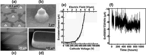
Excellent electric field-induced electron emission from N-UNCD film surfaces [Citation58–61], enables field emitter cold cathodes [Citation61], field emitter flat panel displays [Citation61], and other devises involving electron emission from cathodes shaped as sharp tips (and (b)) or flat edged structures (and (d). Three important properties were demonstrated for N-UNCD-based electron field emission cathodes, namely: i) N-UNCD films exhibit one of the lowest electric field (∼2 V/µm – see ), for emission onset demonstrated today, for both, the conventional sharp field emitter tips and flat edged structures, the latest providing a much lower cost for electron emission manufacturing process, than the more complex and costly fabrication of field emitter tips [Citation61]; iii) the N-UNCD films reported in [Citation61] were the field emitter with the longest stable emission (1000 hrs.) current demonstrated today ().
Figure 17. SEM images: low magnification (a) and high magnification (b) N-UNCD-coated Si tips; low magnification (c) and high magnification (d) edge structures; (e) electron emission current vs. electric field for N-UNCD-coated Si cathodes shown in (a-d); (f) electron emission current vs. time for an array of N-UNCD-coated Si tips.
3.5. Key UNCD Coating-Based medical devices and prostheses
3.5.1. Not yet commercialized UNCD Coating-Based technologies
The UNCD films exhibit what potentially is the best biocompatibility for external and more importantly implantable medical devices. The key reason why UNCD films may be so biocompatible is because they are made of Carbon (C) atoms, which is the element of life in the human DNA, cells, and molecules. Key properties already demonstrated for use in medical devices include
Excellent chemical tailoring via bio-functionalization of the UNCD films’ surface by electrochemical reduction of aryl-diazonium salts to enable efficient/dense growth of biomolecules on the UNCD surface [Citation62].
Excellent biological properties, demonstrated by DNA-induced modification of UNCD thin films surfaces [Citation63], providing stable, biologically active scaffolds for biological cell growth and differentiation [Citation64, Citation65].
Cardiovascular and other Blood Interfacing Devices/Prostheses: Catheters, vascular grafts, stents, and artificial heart valves, are widely used for treatment of cardiovascular diseases, where blood is in contact with the prostheses surface. Thrombus formation (blood clogging aggregates via adhesion of blood platelets/proteins on hydrophilic (fluid adhesion) devices’ surfaces) stops blood flow, inducing failure of devices [Citation66]. Highly hydrophobic (water drop contact angle of ∼120˚) coatings’ surfaces repel fluids, providing self-cleaning, antifouling and/or anticorrosive effects [Citation67], reducing risks of contamination and infections in patients [Citation67]. In this sense, Auciello’s group recently demonstrated that 5 minutes CF4 plasma produces a UNCD coating with a superhydrophobic surface (highest water drop contact angle demonstrated today of ∼178˚) [Citation68], which will enable new generations of devices described above.
3.5.2. Advanced state of development for commercialization of UNCD Coating-Based technologies for medical devices and prostheses
1) Uncd-Encapsulated silicon (Si) microchip implantable in human eye as artificial retina restoring partial vision to blind people.
Excellent biocompatibility (demonstrated in the application of UNCD coatings for encapsulation of a Si microchip implantable in the eye [Citation69] to restore partial vision to people blind by genetically induced death of photoreceptors (condition known as retinitis pigmentosa). Photoreceptors absorb photons from images outside the eye and transform them into electronic charges injecting into the bipolar cells, which amplify the charges and inject them into the ganglion cells, which transfer the charges to the brain via their axons, to form images (). Photoreceptors can be destroyed by a gene () [Citation70, Citation71], leading to the condition known as retinitis pigmentosa, resulting in blindness [Citation70, Citation71]. The gene does not affect the bipolar and ganglions cells. Auciello participated in a 10-years project (2000-2010) [Citation70, Citation71], involving physicists, materials scientists, chemists, electronic engineers, medical doctors and surgeons, to develop an artificial retina to restore partial vision to people blind by retinitis pigmentosa. The R&D performed by Auciello’s group focused on developing encapsulation of a Si microchip with UNCD coating to inhibit chemical corrosion of Si by the eye saline humor and enable implantation inside the eye for years. The UNCD coating is the only one that can be used for encapsulating a Si microchip, because is the only one that can be grown at ≤ 400 °C [Citation72, Citation73], whiting the thermal budget of Si chips, without destroying them. The UNCD-encapsulated Si chip, with large array of integrated electrodes, can be implanted on the retina surface, at the ganglion cell layers (), receiving images from a CCD camera outside the eye, processing the image and injecting electrons on the ganglion cells, which transfer them to the brain through their axons, to form image and return partial vision to blind people. The Si chip is chemically etched by the eye humor. The UNCD coating () eliminates this problem and enables implantation inside the eye for years ().
Figure 18. (a) Schematic showing key eye’s components (lens, retina and optical nerve) responsible for vision; (b) Si microchip coated with UNCD receives images from a CCD camera and process the images into electronic charges that are injected on the ganglion cells, via electrically conductive/eye’s humor corrosion resistant N-UNCD coated large array of Si or metallic tips, and transferred through cells axons (optic nerve), to the brain to form images; (c) cross-section SEM image of insulating/high density/pinhole free/corrosion resistant UNCD coating encapsulating Si chip; (d) (top) SEAM image of UNCD coating surface before implantation of UNCD-encapsulated Si chip in rabbit eye, (middle) UNCD-encapsulated Si chip implanted in rabbit’s eye for 3 years (bottom), SEM image of UNCD coating surface after 3 years implantation, with no degradation at all.
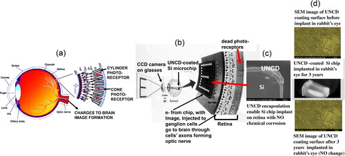
The Argus II device, developed in a 10-year R&D project [Citation69–72], is currently implanted commercially by Second Sight [Citation74] in the USA and Europe, returning partial vision to people blind by retinitis pigmentosa. A detailed description of the materials science, including the R&D on the UNCD coating [Citation69–72], and device development and animal studies and clinical trials in humans [Citation70–75], can be found in the cited references.
Uncd-Coated dental implants (DI)
In the 1980s, Brånemark and colleagues, discovered the phenomenon of metal integration with bones, naming it osseointegration, related to Ti-alloys extensively investigated initially for dental implants [Citation76, Citation77]. Titanium (Ti) or Ti-based alloys are currently widely used to make different prostheses fabricated to replace degraded or destroyed natural components of the human body (e.g. teeth, hips, knees and other joints). Ti or Ti-alloys are used for implants because early R&D indicated that these materials exhibited some biocompatibility and would be resistant to the chemical and mechanical environment of the body. However, in recent years, academic, industrial and medical researchers demonstrated that metal-based (particularly Ti-alloys) prostheses exhibit failures, induced by synergistic mechanical/chemical effects induced by the human body environment (see selected references from 100 s published [Citation78–80]. For DIs, needed to replace degraded natural teeth (and (b)), recent extensive research revealed that Ti-alloy DIs are corroded by oral fluids (), resulting in titanium dioxide (TiO2) particles ejected from the oxidized Ti surface (Ti/Ti-alloys gets easily oxidized upon exposure to atmospheric environment before implantation) are dislodged and inserted into surrounding tissue, inducing inflammation and tissue death (necrosis), as shown for Ti-alloy dental implants [Citation78]. In addition, TiO2 particles were seen in the blood stream and human organs (e.g. liver, spleen, and abdominal lymph nodes) [Citation81, Citation82], producing serious biological deleterious effects. Recent studies by Auciello et al. showed that TiO2 induced necrosis in liver and renal hyaline cylinders of rats, while UNCD particles did not induce any damage at all [Citation82].
Figure 19. (a) picture of natural teeth destroyed by bacteria; (b) picture of Ti-alloy DIs inserted in a patient’s maxillary bone; (c) picture of a Ti-alloy extracted from a patient maxillary bone after about 4 years implantation, showing chemical corrosion produced by the oral fluids; (d) cross-section SEM image of a UNCD-coated Ti-alloy DI, showing excellent dense/pinhole-free extremely conformal UNCD coating; e) pictures of UNCD-coated DI in a patients’ maxillary bone, showing an X-ray image (top left), during implantation (top right), after 3 months implantation (middle) and with crown inserted on top (bottom).
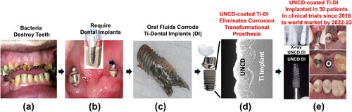
UNCD-coated DIs represent the new transformational DI t3echnology eliminating the failur3e of current metal-based DIs. Dense/pinhole free/oral fluid corrosion resistant UNCD coatings are grown extremely conformally on the screw-type DIs (). UNCD-coated DIs have been implanted in 30 patients, in clinical trials, since 2018, in the world class clinic of Dr. Gilberto López-Chávez. X-ray imaging (-top left) showed excellent osteointegration of a UNCD-coated DI (-bottom left) in the maxillary bone of a patient. (top right) shows a picture of the UNCD-coated DI being implanted in the maxillary bone of the patient. (middle) shows a picture of the top of the UNCD-coated dental implant after three months implantation, being ready for insertion of the ceramic crown (-bottom), which completes the artificial DI insertion into the patient.
The R&D performed to develop the UNCD coating process provided the pathway to produce low-cost coating of up to 250–300 DIs vertically distributed on a 200 mm dimeter holder in the industrial MPCVD system shown in . A detailed description of the R&D for developing the UNCD-coated DIs, animal studies and clinical trials, involving implantation of UNCD-coated DIs in patients can be found in Ref. [Citation83]. UNCD-coated DIs represent the new revolution in DI technology.
3.5. The future: UNCD films for UNCD-based microelectronic devices?
MCD (≥ 1 µm grain size) exhibits high thermal conductivity (∼1900 W/K.m - in Ref. [Citation14]) to provide efficient cooling for the new generation of micro- and nano-electronic devices, based on integrating MCD coating on Si-based microelectronics. On the other hand, NCD (∼10–100 s nm grain size) UNCD (3–5 nm grain size) films exhibit a unique set of multifunctionalities and properties, which can also apply to provide valuable properties for integration with Si-based micro/nanoelectronics. Specifically, UNCD coating has been demonstrated to be the solution to encapsulate a Si-based microchip [Citation69] to be implanted inside the eye, inhibiting the Si microchip of being chemically destroyed by the eye fluid and function as an artificial retina to restore partial vision to people blind by genetically induced degeneration of the photoreceptors [Citation70, Citation71]. In relation to integration of MCD to UNCD films with Si-based micro/nanoelectronics devices, it is critical to be able to grow those films on key components, in film form, of Si-based devices such as CMOS devices. Current Si-based CMOS devices include HfO2 as the main insulating oxide layer [Citation84], as the key component of the gates of CMOS devices and any other Si-based transistors.
Based on the information presented above it is relevant to integrate MCD to UNCD films with HfO2 layers on Si, since HfO2 is the main insulator oxide used in the gates of Si-based CMOS and other micro/nanoelectronics devices today. In relation to this hypothesis, Auciello’s group demonstrated for the first time the integration of UNCD and MCD films on HfO2 layers grown on Si, via Atomic Layer Deposition (ALD) [Citation85]. HfO2 films of 5, 10, 30 and 100 nm, thicknesses were grown on Si substrates heated to 100 °C, using nitrogen purge of 20 s between each ALD precursor pulsing [Citation85] All substrates with the HfO2 layers on the surface were subjected to a diamond seeding process via immersion in a commercial (Nanodiamond Laboratory, NC, USA) solution of methanol with functionalized diamond nanoparticles (to avoid seed particles agglomeration to induce high density pinhole free diamond films), in an ultrasound generator, which insert UNCD (3-5 nm) particles from the seeding solution on the substrate surface via sound waves induced vibration [Citation14]. MCD and UNCD films were grown on the HfO2/Si substrate, using the HFCVD technique described in Section 2.4 of this article. The gases flows used to grow the diamond films were: i) for MCD and NCD films- CH4 (3 sccm)/H2 (200 sccm) during 8 hrs. and 4 hrs., respectively, and for UNCD films-CH4 (2 sccm)/H2 (10 sccm)/Ar (90 sccm) during 1 hr., keeping the total chamber pressure at 10 Torr. The filaments were heated to ∼2200 °C, and the substrate were heated to ∼800 °C for MCD and NCD films growth at ∼650 °C for UNCD film growth, as measured by a calibrated thermocouple in contact with the substrate. The details of the HFCVD process to grown MCD to UNCD films can be found in a recent paper [Citation85]. The micro/nanostructures (grain morphology and size) and films thickness were characterized using scanning electron microscopy (SEM, ZEISS SUPRA-40) and high-resolution transmission electron microscopy (HRTEM, JEOL 2100 F).
The crystallinity and grain sizes of the MCD and UNCD films were determined via X-ray diffraction (XRD, Rigaku Ultima III, Cu Kα radiation, 1.542 Å). The films’ thicknesses were measured via cross section SEM. Chemical bonding in the films were analyzed via visible and UV Raman spectroscopy, The crystal structures of the films were analyzed using selected area electron diffraction (SAED) in HRTEM, and the surface chemistry was characterized using X-ray photoelectron spectroscopy. shows a cross-section HRTEM image of the Si/HfO2/UNCD interfaces. The cross-section image, supported by XPS analysis, shown in , revealed that C atoms, generated from cracking of the CH4 molecules on the hot filament surface, react chemically with Hf, forming a HfC template layer that nucleate the growth of the UNCD to MCD films [Citation85]. and (e) show top and inserted cross-section images of UNCD films grown on SiO2, WOx, and TixAL1-xO3 oxides template layers grown on Si substrates, demonstrating that the best template layer, forming highest dense UNCD films, is the WOx layer, which correlates very well with the prior demonstration that extremely dense MPCVD grown UNCD films are grown on W template layers [Citation14]. On the other hand, and (h), show UNCD, NCD, and MCD films, respectively, grown by HFCVD, on HfO2 template layers on Si substrates, demonstrating that the HfO2 template layer induce the growth of extremely dense UNCD, NCD, and MCD films, which provides a potential pathway for integration of all these films with Si substrates, to enable future integrated Si/diamond micro/nonelectronic devices.
Figure 20. (a) Cross-section HRTEM image of Si/HfO2/UNCD interfaces, showing the formation of nanolaminates of HfC at the HfO2/UNCD interface, proven to be the UNCD nucleation template layer that induce the growth of not only UNCD, but also NCD, and MCD films (see (f), (g), and (h)). Top and inserted cross-section SEM images show that UNCD films grown on SiO2 (c), WOx, and TixAL1-xO3 template layers on Si substrates, exhibit different structure, with the UNCD films on the WOx layer exhibiting the densest structure among the three template layers. Figures (f), (g), and (h) show top and inserted cross-section SEM images of extremely dense UNCD, NCD, and MCD films, respectively, grown on HfO2 template layers.
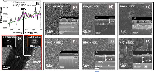
Finally, shows a comprehensive comparison of electronic properties of UNCD, NCD, and MCD films, grown, via the HFCVD process, on Si substrates, and processed into devices, as shown in the schematic on the right side of the figure, used to do the measurements of the electronic performance shown in the figure.
The information and initial data presented above on the integration of UNCD, NCD, and MCD films with Si substrates shows the potential for the development of integrated diamond/Si-based micro/nano-electronics devise sometime in the future.
Table 5. Electronic properties of UNCD, NCDE, and MCD films grown on Si substrates, using the HFCVD process [Citation85].
4. Conclusions
There are key conclusions related to the UNCD coating technology:
Fundamental and applied science performed on the synthesis and properties of the novel material named UNCD, in thin film (coating) form, since its invention in the early 90s, and numerous applications demonstrated until now and those upcoming in the future, have proven that UNCD represents a new paradigm material in film (coating) form, which exhibits a broad range of functionalities applicable to a large range of multifunctional industrial, high-tech and medical devices/prostheses. Many groups worldwide are now working on the science and technology of UNCD coatings, which provides the pathway for substantial advances in the future.
R&D performed in the past twenty years demonstrated that UNCD and electrically conductive N-UNCD and B-UNCD films (coatings) are produced, by MPCVD and HFCVD processes, with extremely uniform nanostructure and thickness across large area substrates, enabling low-cost UNCD coating based industrial, high-tech, and medical products.
Following the development of the UNCD coating technology, Auciello/Carlisle trademarked de name UNCDTM when founding Advanced Diamond Technologies, Inc. (2003, profitable in 2014 and sold for profit to a large company in 2019), the only company marketing worldwide UNCD-coated industrial products (UNCD-coated mechanical pump seals and bearings, AFM tips, and water purification systems with electrically conductive/water corrosion resistant B-UNCD-coated metal electrodes used in electrolysis-based water purification systems). Subsequently, Auciello et al. co-founded Original Biomedical Implants (OBI-USA/2013-present and OBI-México (2016-present), which are developing revolutionary new generations of external and implantable medical devices
The next frontier is the application of UNCD coatings as a unique biocompatible material, made of C atoms (element of life in all human DNA and molecules). UNCD-coated dental implants are in advanced state of clinical trials (30 patients received UNCD-coated dental implants, which are demonstrating far superior performance compared with current metal-based implants). The clinical trials are being conducted by Original Biomedical Implants (OBI-USA and OBI-México). Electrically conductive N-UNCD coating on commercial NG/Cu anodes demonstrated the feasibility of producing a new genertion of long-life, stable capacity energy vs charge/discharge cycles and order of magnide safer LIBs than current LIBs thus providing the opportunity for producing, new generation of defibrillators/pacemakers with > 10x longer life and safer than current technology).
Section 3.5 shows a summary review of initial results on growth of UNCD, NCD, and MCD films on Si substrates, using both the MPCVD and HFCVD process, revealing promising structural, physical, chemical, and electronic properties of the Integrated UNCD, NCD, MCD films/Si substrates, providing potential pathways for development of future integrated diamond/Si micro/nanoelectronics devices.
Acknowledgments
O. Auciello acknowledge different sources, which supported the science and technological applications of the UNCD coatings, during the last twenty years, namely: Distinguished Endowed Chair Professor Grant from University of Texas-Dallas; SENACYT-Panamá, Department of Energy-Basic Energy Sciences Grants, DARPA Grants, ONR Grants, National Science Foundation Grants, and Industrial funding (Rubio-Pharma-México, UHV-Nanoranch, Samsung, INTEL, Lam, Lockheed-Martin). He also acknowledges the contributions of the three main scientists that jointly with him performed the R&D to develop the UNCD coating technology using the MPCVD method, namely: D.M. Gruen, A.R. Krauss, and J.A. Carlisle at Argonne National Laboratory. He also acknowledges the contributions to the R&D related to the HFCVD processing of UNCD films, described in this review, namely: E. de Obaldia, J.J. Alcantar-Peña, J.F. Veyan, M.J. Yacamán, M.J. Arellano-Jimenez, K. Kang, J. Montes-Gutierrez, P. Tirado. A. G. Montaño-Figueroa.
Disclosure statement
No potential conflict of interest was reported by the author(s).
Additional information
Notes on contributors
Orlando Auciello
Orlando Auciello graduated with honors (M.S. (1973), Ph.D. (1976) degrees in Physics from Physics Institute “Dr. Balseiro” (Universidad Nacional de Cuyo-Argentina). EE-University Córdoba-Argentina 1969). Postdoctoral-McMaster University, Canada (1977-1979); Researcher-University of Toronto-Canada (1979-1984), Associate Professor-NCSU-USA (1984-1988), Distinguished Scientist-MCNC-USA (1988-1996), Distinguished Argonne Fellow (1996-2012)-ANL-USA, Distinguished Professor-University Texas-Dallas, Auciello is directing basic and applied research on multifunctional oxide [ferroelectric (piezoelectric), high-K dielectrics films], and nanocarbon films (novel Ultrananocrystalline Damond (UNCDTM) and graphene) and application to industrial, high-tech, and medical devices/prostheses, marketed by ADT (2003, sold for profit in 2019), and Original Biomedical Implants (OBI-USA and OBI-México, all co-founded by Auciello and colleagues. Auciello edited 32 published 560 articles in several fields, holds 23 patents, He was associate editor of APL, and currently of Functional Diamonds, Integrated Ferroelectrics. and Coatings He was President of the Materials Research Society (2013) Auciello is Fellow of AAAS and MRS and has numerous Awards. e-mail: [email protected].
References
- Spitsyn BV, Bouilov LL, Derjaguin BV. Vapor growth of diamond on diamond and other surfaces. J Cryst Growth 1981;52:219–226.
- Matsumoto S, Sato Y, Tsutsumi M, et al. Growth of diamond particles from methane-hydrogen gas. J Mater Sci. 1982;17(11):3106–3112.
- Matsumoto S. “Development of CVD Diamond Synthesis Techniques”, In: Proc. of 1st Symposium on Diamond and Diamond-like Films, Electrochem. Soc. Proc., New York. vol. 50. 1989. p. 89.
- Kamo M, Sato Y, Matsumoto S, et al. Diamond synthesis from gas phase in microwave plasma. J Cryst Growth. 1983;62(3):642–644.
- Matsumoto M, Hino M, Kobayashi T. Synthesis of diamond films in a RF induction thermal plasma. Appl Phys Lett. 1987;51(10):737–739.
- Kurihara K, Sasaki K, Kawarada M, et al. High-rate synthesis of diamond by DC plasma jet chemical vapor deposition. Appl Phys Lett. 1988;52(6):437–438.
- Dischler B, Wild C. Low-Pressure synthetic diamond: manufacturing and applications. Heidelberg: Springer; 1998.
- Butler JE, Sumant AV. The CVD of nanodiamond materials. Chem Vap Deposition. 2008;14(7-8):145–160. vol
- Gruen DM, Liu S, Krauss AR, et al. Fullerenes as precursors for diamond film growth without hydrogen or oxygen additions. Appl Phys Lett. 1994;64(12):1502–1504.
- Smalley RE. Discovering the fullerenes. Rev Mod Phys. 1997;69(3):723–730.
- McCauley TG, Corrigan TD, Krauss AR, et al. Electron emission properties of Si field emitter arrays coated with nanocrystalline diamond from fullerene precursors. In: Proc. MRS, Symposium. “Electron Emission from Highly Covalent Materials.” vol. 498, 1998. p. 227.
- Jiao S, Sumant AV, Kirk MA, et al. Microstructure of ultrananocrystalline diamond films grown by microwave Ar–CH4 plasma chemical vapor deposition with or without added H2. J Appl Phys. 2001;90(1):118–122.
- Naguib N, Birrell J, Elam J, et al. A method to grow carbon thin films consisting entirely of diamond grains 3-5 nm in size and high-energy grain boundaries. US Patent #7,128,8893, 7,556,982. 2006.
- Auciello O, Sumant AV. Status review of the science and technology of ultrananocrystalline diamond (UNCDTM) films and application to multifunctional devices. Diamond Relat Mater. 2010;19(7-9):699–718.
- Shenderova OA, Gruen DM. Ultrananocrystalline diamond: Synthesis, properties and applications. Oxford, UK: Elsevier; 2006.
- May PW, Harvey JN, Smith JA, et al. Re-evaluation of the mechanism for ultrananocrystalline diamond deposition from Ar∕CH4∕H2 gas mixtures. J Appl Phys. 2006;99(10):104907.
- Xu Z, He Z, Song Y, et al. Topic review: Application of raman spectroscopy characterization in micro/nano-machining. Micromachines (Basel). 2018;9(7):361.
- Birrell J, Gerbi JE, Auciello O, et al. Interpretation of the Raman spectra of ultrananocrystalline diamond. Diamond Relat Mater. 2005;14(1):86–92.
- Zuiker D, Krauss AR, Gruen DM, et al. Characterization of diamond thin films by core-Level photo-absorption and UV excitation Raman spectroscopy. Mat Res Soc Proc. 1996;437:211.
- Sumant AV, Auciello O, Liao M, et al. MEMS/NEMS based on Mono, nano, and ultrananocrystalline diamond films. MRS Bull. 2014;39(6):511–516.
- Stoner BR, Ma G-HM, Wolter SD, et al. Characterization of bias-enhanced nucleation of diamond on silicon by in vacuo surface analysis and transmission electron microscopy. Phys Rev B. 1992;45(19):11067–11084.
- Gerber S, Sattel S, Ehrhardt H, et al. Investigation of bias enhanced nucleation of diamond on silicon. J Appl Phys. 1996;79(8):4388.
- Lee YC, Lin SJ, Chia CT, et al. Effect of processing parameters on the nucleation behavior of nano-crystalline diamond film. Diamond Relat Mater. 2005;14(3-7):296–301.
- Chen YC, Zhong XY, Konicek AR, et al. Synthesis and characterization of smooth ultrananocrystalline diamond films via low pressure bias-enhanced nucleation and growth. Appl Phys Lett. 2008;92(13):133113.
- Zhong XY, Chen YC, Tai NH, et al. Effect of pretreatment bias on the nucleation and growth mechanisms of ultrananocrystalline diamond films via bias-enhanced nucleation and growth: an approach to interfacial chemistry analysis via chemical bonding mapping. J Appl Phys. 2009;105(3):034311.
- Ding MQ, Krauss R, Auciello O, et al. Studies of field emission from bias-grown diamond thin films. J Vac Sci Technol B. 1999;17(2):705–709.
- Bhattacharyya S, Auciello O, Birrell J, et al. Synthesis and characterization of nitrogen doped ultrananocrystalline diamond thin films. Appl Phys Lett. 2001;79(10):1441–1443.
- Gruen DM, Krauss AR, Auciello O, et al. N-Type doping of NCD films with nitrogen and electrodes made there from US patent # 6,793,849 B1. 2004.
- Birrell J, Carlisle JA, Auciello O, et al. Morphology and electronic structure in nitrogen-doped ultrananocrystalline diamond. Appl Phys Lett. 2002;81(12):2235–2237.
- Zapol P, Sternberg M, Curtiss LA, et al. Tight binding molecular dynamics simulation of impurities in ultranancrystalline diamond grain boundaries. Phys Rev B. 2001;65(4):045403.
- Heck PR, Staderman FJ, Isheim D, et al. Atom-Probe analyses of nano-diamonds from allende. Meteorit Planet Sci. 2014;49(3):453–467.
- Fuentes-Fernandez EMA, Alcantar-Peña JJ, Lee G, et al. Synthesis and characterization of microcrystalline diamond to ultrananocrystalline diamond films via hot filament chemical vapor deposition for scaling to large area applications. Thin Solid Films. 2016;603:62–68.
- Alcantar-Peña JJ, de Obaldia E, Montes-Gutierrez, Kang K, et al. Fundamentals towards large area synthesis of multifunctional ultrananocrystalline diamond films via large area hot filament chemical vapor deposition bias enhanced nucleation/bias enhanced growth for fabrication of broad range of multifunctional devices. Diamond Relat Mater. 2017;78:1–11.
- Huang B-R, Chia C-T, Chang M-C, et al. Bias effects on large area polycrystalline diamond films synthesized by the bias enhanced growth technique. Diamond Relat Mater. 2003;12(1):26–32.
- Alves R, Amorim A, Eichenberger Neto J, et al. Filmes de diamante CVD em grandes áreas obtidos por crescimentos sucessivos em etapas. Revista Matéria. 2008;13(3):569–578.
- Weng J, Liu F, Xiong LW, et al. Deposition of large area uniform diamond films by microwave plasma CVD. Vacuum. 2018;147:134–142.
- Suna Q, Wang J. Study on the large area diamond film deposition in a self- built overmoded microwave power chemical vapor deposition device. Chem Eng Transactions. 2017;62:1129–1134.
- Lee ST, Lam YW, Lin Z, et al. Pressure effect on diamond nucleation in a hot-filament CVD system. Phys Rev B. 1997;55(23):15937–15941.
- Schwarz S, Rosiwal SM, Frank M, et al. Dependence of the growth rate, quality, and morphology of diamond coatings on the pressure during the CVD-process in an industrial hot-filament plant. Diamond Relat Mater. 2002;11(3-6):589–595.
- Hao T, Zhang H, Shi C, et al. Nano-crystalline diamond films synthesized at low temperature and low pressure by hot filament chemical vapor deposition. Surf Coat Tech. 2006;201(3-4):801–806.
- Liang X, Wang L, Zhu H, et al. Effect of pressure on nanocrystalline diamond films deposition by hot filament CVD technique from CH4/H2 gas mixture. Surf Coat Tech. 2007;202(2):261–267.
- Advanced Diamond Technologies, Inc. Advanced Diamond Technologies, Inc. (www.thindiamond.com).
- Uppireddi K, Weiner BR, Morell G. Synthesis of nanocrystalline diamond films by DC plasma-assisted argon-rich hot filament chemical vapor deposition. Diamond Relat Mater. 2008;17(1):55–59.
- Makris TD, Giorgi R, Lisi N, et al. Bias enhanced nucleation of diamond on Si (100) in a vertical straight hot filament CVD. Diamond Relat Mater. 2005;14(3-7):318–322.
- Zhou XT, Lai HL, Peng HY, et al. Heteroepitaxial nucleation of diamond on Si (100) via double bias assisted hot filament chemical vapor deposition. Diamond Relat Mater. 2000;9(2):134–139.
- Janischowsky K, Ebert W, Kohn E. Bias enhanced nucleation of diamond on silicon (100) in a HFCVD system. Diamond Relat Mater. 2003;12(3-7):336–339.
- Pecoraro S, Arnault JC, Werckmann J. BEN-HFCVD diamond nucleation on Si(111) investigated by HRTEM and nano-diffraction. Diamond Relat Mater. 2005;14(2):137–143.
- Li Y, Li J, Wang Q, et al. Controllable growth of nanocrystalline diamond films by hot filament chemical vapor deposition method. J Nanosci Nanotech. 2009;9(2):1062–1065.
- Ansari SG, Anh TL, Seo H-K, et al. Growth kinetics of diamond film with bias enhanced nucleation and H2/CH4/Ar mixture in a hot-filament chemical vapor deposition system. J Cryst Growth. 2004;265(3-4):563–570.
- Auciello O, Pacheco S, Sumant AV, et al. Are diamonds a MEMS best friend? IEEE Microwave. 2007;8(6):61–75.
- Auciello O, Birrell J, Carlisle JA, et al. Materials science and fabrication processes for a new MEMS technology based on ultrananocrystalline diamond thin films. J Phys Condens Matter. 2004;16(16):R539–R552.
- Auciello O, Lee G. Science and technology of integrated piezoelectric oxide/ultrananocrystalline (UNCDTM) films for a new generation of biomedical MEMS/NEMS energy generation, drug delivery and sensor devices. Ch. 9 In: Auciello O, editor. Ultrananocrystalline diamond coatings for new generation High-Tech and medical devices.Cambridge Publisher (in press, June); 2022.
- Lee G, Fuentes-Fernandez EMA, Lian G, et al. Heteroepitaxial BiFeO3/SrTiO3 nanolaminates with higher piezoresponse performance over stoichiometric BiFeO3 films. Appl Phys Lett. 2015;106(2):022905.
- Cheng Y-W, Lin C-K, Chu Y-C, et al. Electrically conductive ultrananocrystalline diamond-coated natural graphite-copper anode for new long-life lithium-ion battery. Adv Mater. 2014;26(22):3724–3729.
- Tzeng Y, Auciello O, Liu C-P, et al. Nanocrystalline-diamond/carbon and nanocrystalline-diamond/silicon composite electrodes for Li-based batteries US Patent # 9,196,905, 2015. 2015.
- Yuan W-X, Wu QX, Luo ZK, et al. Effects of boron doping on the properties of ultrananocrystalline diamond films. J Elec Mater. 2014;43(4):1302–1306.
- Tirado P, Alcantar-Peña JJ, de Obaldia E, et al. Boron doping of ultrananocrystalline diamond films by thermal diffusion process. MRS Commun. 2018;8(3):1111–1118.
- Krauss AR, Ding MQ, Auciello O, et al. Electron field emission for ultrananocrystalline diamond films. J Appl Phys. 2001;89(5):2958–2967.
- Hajra M, Ding M, Auciello O, et al. Effect of gases on the field emission properties of ultrananocrystalline diamond-coated silicon field emitter arrays. J Appl Phys. 2003;94(6):4079–4083.
- Lin YC, Sankaran KJ, Chen YC, et al. Enhancing electron field emission properties of UNCD films through nitrogen incorporation at high substrate temperature. Diamond Relat Mater. 2011;20(2):191–195.
- Getty SA, Auciello O, Sumant AV, et al. Characterization of nitrogen-incorporated ultrananocrystalline diamond as a robust cold cathode material. In: George T, Islam S, and Dutta A, editors. Micro-and nanotechnology sensors, systems, and Applications-II., Proc. SPIE. vol. 7679. 2010; p. 76791N-1.
- Wang J, Firestone MA, Auciello O, et al. Surface functionalization of ultrananocrystalline diamond films by electrochemical reduction of aryl diazonium salts. Langmuir. 2004;20(26):11450–11456.
- Yang W, Auciello O, Butler JE, et al. Preparation and Electrochemical Characterization of DNA-modified Nanocrystalline Diamond Films. Mat Res Soc Symp Proc. 2007; 737: F4 4. 1–4.6.
- Bajaj P, Akin D, Gupta A, et al. Ultrananocrystalline diamond film as an optimal cell interface for biomedical applications. Biomed Microdevices. 2007;9(6):787–794.
- Shi B, Jin Q, Chen L, et al. Fundamentals of ultrananocrystalline diamond (UNCD) thin films as biomaterials for developmental biology: embryonic fibroblasts growth on the surface of (UNCD) films. Diamond Relat Mater. 2009;18(2-3):596–600.
- Jaffer H, Fredenburgh JC, Hirsh J, et al. Medical device-induced thrombosis: what causes it and how can we prevent it? J Thromb Haemost. 2015;13(1):S72–S81.
- Hughes E. Advances in hydrophilic and hydrophobic coatings for medical devices. Med Des Briefs Mag. 2017.
- Gabriela Montano-Figueroa A, Alcantar-Peña JJ, Tirado P, et al. Tailoring of polycrystalline diamond surfaces from hydrophilic to superhydrophobic via synergistic chemical plus microstructuring processes. Carbon. 2018;139:361–368.
- Xiao X, Wang J, Carlisle JA, et al. In vitro and in vivo evaluation of ultrananocrystalline diamond for coating of implantable retinal microchips. J Biomed Mater Res. 2006;77B(2):273–281.
- Humayun MS, Dorn JD, da Cruz L, et al. Interim results from the international trial of second sight’s visual prosthesis. Ophthalmology. 2012;119(4):779–788.
- Zhou DD, Greenberg RJ. Microelectronic visual prostheses, biological and medical physics, biomedical engineering: Implantable neural prostheses 1: Devices and applications. Zhou DD, Greenbaum E, editors. Springer; 2010.
- Xiao X, Birrell J, Gerbi JE, et al. Low temperature growth of ultrananocrystalline diamond. J Appl Phys. 2004;96(4):2232–2239.
- Carlisle JA, Gruen DM, Auciello O, et al. A method to grow pure nanocrystalline diamond films at low temperatures and high deposition rates US Patent # 7,556,982, 2009. 2009
- Second Sight. Second Sight (https://secondsight.com).
- Auciello O. Ultrananocrystalline diamond (UNCD) films as hermetic biocompatible/bioinert coating for encapsulation of eye implantable microchip to restore partial vision to blind people. Ch. 2 In: Auciello O, editor. Ultrananocrystalline diamond coatings for new generation High-Tech and medical devices. Cambridge Publisher (in press); June 2022.
- Brånemark PI, Zarb G, Albrektsson T, (Eds) Introduction to osseointegration tissue-integrated prostheses - osseointegration in clinical dentistry. Chicago: Quintessence Publishing, Co., Inc; 1985; p. 11.
- Ericsson I, Glantz PO, Brånemark PI. Titanium implants of brånemark type for oral rehabilitation of partially edentulous patients. Tandlakartidningen. 1989;81(24):1357.
- Jacobs JJ, Gilbert JL, Urban RM. Current concepts review: corrosion of metal orthopaedical implants. J Bone Joint Surg. 1998;80:268.
- Olmedo DG, Tasat D, Evelson P, et al. Biological response of tissues with macrophagic activity to titanium dioxide. J Biomed Mater Res Part A. 2008;84(4):1087–1093.
- Rodriguez DC, Valderrama P, Wilson T, et al. Titanium corrosion mechanism in the oral environment: a retrieval study. Materials. 2013;6(11):5258–5274.
- Urban R, Jacobs J, Tomlinson M, et al. Dissemination of wear particles to the liver, spleen, and abdominal lymph nodes of patients with hip or knee replacement. J Bone and Joint Surg. 2000;82(A):457.
- Tasat DR, Bruno ME, Domingo M, et al. Biokinetics and tissue response to ultrananocrystalline diamond nanoparticles employed as coating for biomedical devices. J. of Biomedical Materials: Applied Biomaterials. 2016;008:1.
- Kang K, Auciello O, Olmedo DG, et al. “Science and Technology of Biocompatible Ultrananocrystalline Diamond (UNCDTM) Coatings for New Generation of Implantable Prostheses: First Application to Dental Implants and Artificial Hips”, Ch. 5 In: Auciello O, editor. Ultrananocrystalline diamond coatings for new generation High-Tech and medical devices., Cambridge Publisher (in press); June 2022.
- Robertson J. Phys E. High dielectric constant oxides. Eur Phys J Appl Phys. 2004;28(3):265–291.
- Alcantar-Peña JJ, Lee G, Fuentes-Fernandez EMA, et al. Science and technology of diamond films grown on HfO2 interface layer for transformational technologies. Diamond Relat Mater. 2016;69:221–228.