
Abstract
Diamond and graphene are considered to be one of the most promising thermal interface materials (TIMs) for electronic devices benefited from their highest thermal conductivity in the natural world. However, orientated fabrication of high thermal conductivity diamond and graphene hybrid arrays with three dimensions (3 D) thermal conductive networks are still problematic. Here, we used a unique one-step microwave plasma chemical vapor deposition, n-butylamine, as the liquid source to prepare a novel high thermal conductivity 3 D vertical diamond/graphene (VDG) hybrid arrays films. The orientated 3 D thermal conduction path of the VDG is regulated by the growth temperature, and the through-plane thermal conductivity value of the VDG700 films up to 97 W m−1 K−1. In the actual TIM performance measurement, the system cooling efficiency with our VDG as TIM is higher than the state-of-the-art commercial TIM, demonstrating the superior ability to solve the inter-facial heat transfer issues in electronic systems.
1. Introduction
“Overheating” is a major problem in the modern electronics industry because of miniaturized and lightened gradually, which can seriously affect the service life and normal operation of the devices [Citation1–3]. It is well known that micro gaps are filled with air, which is seriously affected heat dissipation. Thermal interface materials (TIMs), such as phase change materials and thermal pads, hold a dominant position for rapid heat transfer in microelectronics and microsystems [Citation4–7]. Numerous studies have shown that diamond and graphene composites, by other methods such as annealing, vapour deposition, laser melting and high temperature, and high pressure [Citation8–10], exhibit good mechanical properties and high electrical conductivity, show great application potential as TIMs in the natural world [Citation11].
Traditional carbon-based TIMs are made by filling diamond particles, graphene nanosheets, and carbon nanotube (CNT) array into an organic polymer matrix [Citation12–14], and also methods of injecting polymers into diamond foam skeletons, graphene networks, vertical arrays of structured graphene paper, and CNT [Citation15–18]. On comparison, carbon-based TIMs with a vertical alignment of 3 D materials, instead of random orientation, are highly desirable to break through the performance bottleneck of current TIMs. To obtain vertically aligned architecture of TIMs, researchers have done many works, including, graphene paper lateral stacking [Citation18], constructed by in situ growth [Citation19], electric field-assisted [Citation20], and chloroform-assisted methanol-based plasma enhancement [Citation21,Citation22], etc. However, it is still difficult to achieve batch production due to the complexity and the less practicality.
Here, a unique one-step growth of VDG films using microwave plasma chemical vapor deposition (MPCVD) is presented, where a liquid organic compound- n-butylamine acts as the single reactive source. The unique 3 D thermal conduction path of the VDG is regulated by the growth temperature in a single step. The actual heat and finite element simulation methods are performed for the analysis of the heat conductivity mechanism.
2. Experimental
2.1. Growth of VDG films with MPCVD
3D hybrid VDG films were grown on a silicon substrate by the self-developed stainless steel ring resonator of a 15 kW power MPCVD (Herui Microwave) system (Text S1, Supporting Information). The n-butylamine (C4H11N) is stored in a stainless steel tank and introduced into the deposition chamber by the pressure difference between the stainless steel tank and the deposition chamber. First, H2 is fed into the MPCVD equipment. With the temperature and pressure rising slowly until a metastable state is reached (that is, there is a difference of about 150 °C between the growth temperature and the pressure is stable at 6–7 kPa), the liquid source n-butylamine with the valve scale of “6” is fed into the equipment. While the liquid source continues to enter, the equipment starts to heat up and pressure boost. About 15 min later, the liquid source flux with the valve scale of “8” was continued to flow into the valve, and the power was slightly adjusted to the required growth temperature. After 3 h of steady state, the liquid source was closed, and the pressure and temperature were lowered slowly at random. Samples were taken out and the equipment was shut down. During the experiment, the growth temperatures of VDG films were set at 600 °C, 700 °C, and 800 °C, and they were named VDG600, VDG700, and VDG800, respectively. Detailed growth parameters are shown in .
Table 1. Growth parameters of VDG films.
2.2. Characterization
The microstructural of the films was observed using field emission scanning electron microscopy (SEM) and high-resolution transmission electron microscopy (TEM), the chemical bonding states of the VDG films were also analyzed using electron energy loss spectroscopy (EELS). The crystal structure and surface chemical compositions were determined using grazing incidence X-ray diffractometer (GI-XRD) measurements performed with an incident angle of 1.5°, a Raman spectrometer with a laser wavelength of 514.5 nm, and X-ray photoelectron spectroscopy (XPS), respectively. The growth process of gas cleavage was monitored by optical emission spectrometer (OES, PG2000-pro). The thermal conductivity was measured by using a laser flash apparatus (GB/T 22588-2008).
3. Results and discussion
3.1. Characterization of VDG films
The content and size structure of diamond and graphene are very important for the construction of high thermal conductivity network structure. As shown in , the growth rate of VDG600 film along each direction does not change much, and equiaxed grains with a thickness of about 18 μm are obtained. The anisotropic growth of the VDG700 and VDG800 films is obvious, forming needle-like structures [Citation23], with the height of both being 30 and 32 μm, respectively. Depending on the transverse morphology of the VDG films developing under different power densities, it is possible to observe that the film is completely perpendicular to the substrate.
Figure 1. (a)–(c) the SEM images of the films at VDG600, VDG700, and VDG800, respectively (The illustration shows the cross sectional SEM images). (d)–(f) the TEM profile images of VDG600, VDG700, and VDG800 films, respectively.
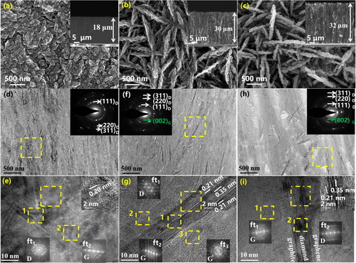
The surface topographies of VDG films were investigated by TEM in , the selected area electron diffraction (SAED) diagram illustrates that the corresponding bright rings are diamond phase (111)D, (220)D, (311)D and graphene phase (002)G crystalline surfaces. The adjacent crystalline planes are 0.20 nm, which is similar to the theoretical spacing value of the (111)D crystalline planes of the diamond phase, indicating that is diamond; and 0.34 nm of adjacent crystalline planes shows the existence of graphene. The Fourier transform the image also verifies the diamond and graphene phase. The difference between the three samples is that the graphene phase only appears in the VDG700 and VDG800. shows the “heart-shell” structure of the diamond coated with graphene, and this microstructure connects the diamond very well with graphene, which provides favourable conditions for the transfer of heat between phonons [Citation24].
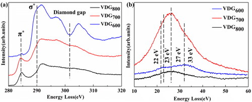
Since it is difficult to distinguish between amorphous and crystallized sp2 bonded carbon in thin films from TEM microstructure studies, in order to fully understand the bonding structure of the films, we combine EELS ( and Text S2, Supplementary Information) with TEM. As what can be seen from the picture, the VDG films surge up to 289.5 eV (σ*-band), while the VDG600 films show a significant drop at 302.0 eV [Citation25,Citation26], indicating the presence of mainly sp3 bonds i.e. diamond in our films. However, the curve at 302.0 eV flattens out as the temperature increases, indicating that the diamond character of the films is diminishing. In addition, the π*-band at 284.5 eV hints the presence of sp2 bonds in the VDG films. The π*-band at 284.5 eV of VDG800 sample is significantly more intense than VDG700, suggesting that a larger proportion of sp2 bonded carbon is induced in the higher temperature films [Citation27], while the small π*-band intensity of the VDG600 film is an indirect evidence that its composition is almost free of graphite phases. The nature of sp2 bonded carbon was further explored through plasma loss EELS spectroscopy, as shown in , the graphite phase has a distinct peak at s3 (27 eV) and the α-C phase at s1 (22 eV), while the crystalline sp3 bonded carbon (diamond), there is a peak at s4 (33 eV) corresponding to bulk plasma loss and a shoulder at s2 (23 eV) corresponding to surface plasma loss [Citation28]. However, the ionization loss spectra of the VDG600 film are mainly concentrated in the s4 band with less intensity in the s2 and s3 bands, which demonstrates that this sample contains a large amount of diamond; the loss spectra of VDG700 and VDG800 are mainly concentrated in the s3 band, and the VDG700 film has more intensity in the s3 band and less intensity in the s2 and s4 bands, based on this fact, the core loss EELS implies the sp2-bonded carbon is mainly present in the nano-graphite phase, with a small amount of α-C phase. Due to the higher electronic thermal conductivity of nano-graphite compared to α-C phase [Citation29], this provides direct proof for the subsequent differences in thermal conductivity of VDG films at different temperatures. The EELS observations are consistent with the previously observed FIB-TEM microstructure.
Figure 2. (a) core-loss EELS spectra and (b) plasmon-loss EELS spectra of VDG films.
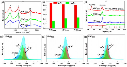
The quality and crystallinity of VDG films were characterized by the Raman test and GI-XRD shown in . For Raman analysis, the two D peaks (1353 cm−1) corresponding to amorphous carbon and the G peak (1584 cm−1) are characteristic peaks of VDG films. The ID/IG (I stands for strength) value can be used to describe the defect degree of the VDG film, and the I2D/IG value can be used to judge the number of graphene layers [Citation30,Citation31]. With increasing the growth temperature, the ID/IG ratio (<1) also increased, indicating that VDG films have a good quality with low defect concentration. Moreover, the high I2D/IG ratio (>1) calculated from the Raman spectrum confirms the good crystallinity and multilayer structure of our samples grown by MPCVD. shows the GI-XRD pattern of VDG films, for VDG600, three distinct diamond peaks (111)D, (220)D and (311)D can be observed at 2θ of 43.9, 75.4, and 91.4°, respectively; at higher temperatures, in addition to the diamond peaks, two graphene peaks (002)G and (110)G can be observed at 26.3° and 78°, which indicates a change in the diamond and graphene content with increasing temperature and also demonstrates the coexistence characteristic of the diamond and graphene phases. Gauss-Lorentz was used to peak the high-resolution XPS spectrum shown in , three sub-peaks located at 284.6, 285.1, and 286.0 eV can be observed in the C1s spectrum, corresponding to sp2-C, sp3-C, and CN/CO bonds [Citation32], respectively. With increasing the temperature, the area of sp2-C and sp3-C peak imply the increase of graphene content and the decrease of diamond, and the content of oxygen and nitrogen-containing groups of VDG films (Text S3, Supporting Information) is extremely low, indicating a very low defect density.
Figure 3. (a) Raman spectra of VDG films. (b) ID/IG and I2D/IG ratios of Raman spectra of VDG films. (c) GI-XRD patterns. (d)–(f) XPS C1s spectrum of VDG films.
3.2. Growth mechanism of VDG films
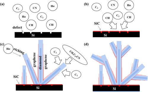
In the process of VDG films growth, the organic liquid small molecule source was heated and evaporated into the MPCVD cavity in a water bath. The whole process of gas cleavage was monitored by OES spectroscopy (). The gas cracking process contains CN (388 nm and 421 nm), C2 (473 nm, 516 nm, and 563 nm), Hα (656.5 nm), Hβ (486 nm) [Citation33]. Since the content of Hβ is almost constant during the temperature change, the relative changes of each ion group during the growth of VDG films are calculated by integration (). The decrease of CH/Hβ indicates that the nucleation of diamond mainly depends on CH. The trend of the CH/Hβ curve demonstrates that diamond nucleation mainly depends on CH. The fact of decreasing of CN/Hβ and C2/Hβ after increasing indicates that they play a decisive role in promoting the nucleation of graphene. The curve of the Hα/Hβ ratio is due to the dissociation of gas carbide. Therefore, the possible growth models of VDG films is plotted in . During the initial stage, the plasma preferentially generates SiC layer on the silicon substrate which contains the defects and CH promotes diamond nucleation, and followed by C2 and CN promoted the graphene nucleation. In addition, a diamond structure coated with graphene is formed with a secondary nucleation process [Citation24,Citation34].
Figure 4. (a) Plasma spectrum of VDG films TIMs. (b) The relationship between the growth temperature, intensity ratio of CH/Hβ, CN/Hβ, C2/Hβ, and Hα/Hβ.
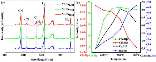
Figure 5. Model of VDG films growth. (a) Under the stimulation of microwaves, the carbon source and hydrogen are transformed into C2, CH, CN, Hα and Hβ. (b) CH and silicon substrate are preferentially combined at the defect to generate SiC. (c) CH promotes the nucleation of diamond based on SiC, and C2 and CN promote the formation of graphene. (d) Secondary nucleation occurs during growth.
3.3. Characterization of the thermal properties of VDG films as TIMs
The thermal conductivity for TIMs were measured via laser flash method (Text S4, Supplementary Information). In , at the same test temperature, the thermal conductivity of VDG600, VDG700, and VDG800 are up to 57, 97, 91 W•m−1•K−1, respectively, which is higher than those of conventional carbon-based TIMs (). With increasing the test temperature, the thermal conductivity value of each sample is basically stable and such difference of the thermal properties can be attributed to the different longitudinal structure of VDG films. The VDG600 film is not conducive to heat transfer in the longitudinal direction because for its vertical array structure is primarily composed of nanoscale clustered carbon structures. The diamond nanowires of VDG700 film have a homogeneous distribution of graphene and diamond morphology, which facilitates heat transfer in a continuous channel. The longitudinal morphology of VDG800 film is in the middle, with the diamond in the form of short rods with a small aspect ratio, and although the graphene component is predominant, it is not as continuous as in VDG700 film. The bonding of individual chemical bonds is entirely responsible for the hybridization of graphene and diamond, which reduces interfacial thermal resistance due to phonon scattering and alleviates barrier to the thermal transport of phonons and electrons.
Figure 6. (a) Thermal conductivity value of VDG films measured by laser flash method. (b) The variation trend of the surface temperature of VDG films tested by a thermocouple (The inset is a schematic diagram of the actual simulation device). (c) LED infrared image integrated with VDG films.
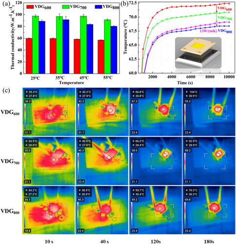
Table 2. Thermal conductivity values of different carbon-based TIMs.
To evaluate the potential of the VDG films as TIMs in electronic devices, a system was designed to simulate heat dissipation in electronic components as shown in , including a thermocouple temperature test and infrared camera photography. In the actual thermal simulation, the samples were mounted separately between a LED lamp (5 W power) and a commercial heat sink (Metal aluminium), and the thermocouple piece is located above the sample, while the infrared thermal imager is located 50 cm above the LED. According to thermocouple temperature data, each sample tends to be stable after about 3000 s. For the temperature of the hottest spot, the maximum temperature of the ceramic plate with VDG800 was 68.4 °C, which was lower than that of the best commercial thermal conductive silicone pad and other VDG films. This result seems to contradict the above values, mainly because in practical applications a common heat dissipation mechanism in the horizontal and vertical directions has to be considered. From the previous analysis of the VDG films composition, it is clear that the VDG films are dominated by graphene components at the high temperature, and the graphene layers rely mainly on van der Waals forces to maintain each other, although the van der Waals forces act weakly and are not conducive to heat propagation between the layers. However, monolayer graphene has a high thermal conductivity. Moreover, because our films have a flake structure in the longitudinal direction, we speculate that the superior heat dissipation of the VDG800 film compared to the VDG700 film is a result of the higher amount of graphene playing a role in heat dissipation [Citation41]. It has been shown that defects can lead to phonon scattering and affect the propagation of heat [Citation42]. From the ID/IG ratio in the Raman spectrum and the GI-XRD results, what can be seen is that the VDG thin film has fewer defects as the temperature increases, in other words, the crystallinity is better, which supports the conclusion that the VDG800 film dissipates heat best.
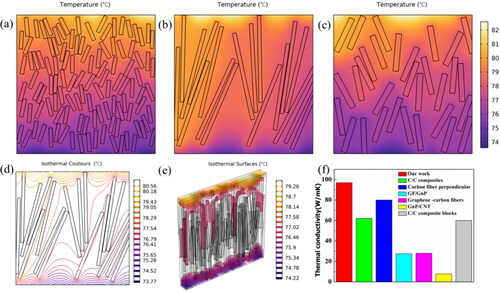
To prove the conductive thermal advantage of these 3 D VDG films, the element simulation methods was used to evaluate the mechanism of VDG films as TIMs (, Text S5 Supplementary Information). The heat source on the upper surface of the sample is 500 W/m2, and the lower surface is exposed to air, with symmetric sides. The thermal conductivity values of three different VDG film TIMs were, respectively, set as 57, 97, 91 W m−1 K−1, and the simulation results were obtained as shown in . As can be seen from the figure, in longitudinal direction, the temperature distribution of VDG700 film TIMs with larger thermal conductivity coefficient was quite different, and the temperature difference was very obvious. It can be observed from the comparison that the "core-shell" VDG composite film used in this study as the TIMs has very good thermal conductivity, highlighting the importance of the vertical array longer thermal conductivity path (, Text S6 Supplementary Information). In addition, the comparison of the thermal conductivity values of different types of carbon-based TIMs along the preferred direction of heat conduction is shown in , indicating that our sample has extremely high values compared with the existing literature.
Figure 7. (a)–(c) Simulation and comparison of heat transfer performance in vertical direction of 600 °C, 700 °C, and 800 °C VDG film TIMs. (d) 2 D and (e) 3 D isotherms of VDG700 film TIMs. (f) Comparison of thermal conductivity values of different carbon-based TIMs.
4. Conclusion
In summary, the VDG films with 3 D thermal conductive networks were successfully prepared using the one-step MPCVD method. Combined with the thermal simulation results and the characteristics of diamond and graphene, it is found that the VDG film TIMs has good thermal conductivity in the transverse and longitudinal direction, which demonstrates that, the VDG film with the “core-shell” structure has a continuous thermal conductivity path, featured with great heat dissipation which is conducive to heat dissipation. The VDG700 film had the highest through-plane thermal conductivity value (97 W m−1 K−1) among the three samples, and the VDG800 film is lower than the silicone pad with the best thermal conductivity on the market according to practical thermal simulation. From the element simulation methods analysis, the VDG700 film indeed has the highest thermal conductivity value in the longitudinal direction. This study provides a simple and practical way of constructing vertically aligned architecture and efficiently improves thermal conductivity for the TIMs application.
Authors’ contributions
Guorong Zhang: Conceptualization, Data analysis, Investigation, Methodology, Visualization, Writing-original draft. Huiqiang Liu: Data curation, Writing-review & editing, Visualization (equal). Yangxin Xiao: Data curation, Visualization. Bing Wang: Formal analysis. Jian Wang: Writing-review & editing. Wen Zhang: Supervision, Data curation. Ying Xiong: Funding acquisition, Investigation, Project administration, Supervision, Writing–review and editing.
Supplemental Material
Download MS Word (2.1 MB)Disclosure statement
The authors declare that they have no known competing financial interests or personal relationships that could have appeared to influence the work reported in this paper.
Additional information
Funding
References
- Yan Q, Alam FE, Gao J, et al. Soft and self‐adhesive thermal interface materials based on vertically aligned, covalently bonded graphene nanowalls for efficient microelectronic cooling. Adv Funct Mater. 2021;31(36):2104062.
- Khan J, Momin SA, Mariatti M. A review on advanced carbon-based thermal interface materials for electronic devices. Carbon. 2020;168:65–112.
- Yu T-P, Lee Y-L, Li Y-W, et al. The study of cooling mechanism design for high-power communication module with experimental verification. Appl Sci. 2021;11(11):5188.
- Ma H, Gao B, Wang M, et al. Strategies for enhancing thermal conductivity of polymer-based thermal interface materials: a review. J Mater Sci. 2021;56(2):1064–1086.
- Chung DDL. Performance of thermal interface materials. Small. 2022;18(16):2200693.
- Li M, Li L, Hou X, et al. Synergistic effect of carbon fiber and graphite on reducing thermal resistance of thermal interface materials. Compos Sci Technol. 2021;212:108883.
- Razeeb KM, Dalton E, Cross GLW, et al. Present and future thermal interface materials for electronic devices. Int Mater Rev. 2018;63(1):1–21.
- Yu S, Liu S, Jiang X, et al. Recent advances on electrochemistry of diamond related materials. Carbon. 2022;200:517–542.
- Jian Z, Xu J, Yang N, et al. A perspective on diamond composites and their electrochemical applications. Curr Opin Electrochem. 2021;30:1–9.
- Zhao G, Yang N, Martínez-Huitle CA. Editorial overview: diamond electrochemistry current advances, challenges and opportunities in diamond electrochemistry. Curr Opin Electrochem. 2022;36:1–5.
- Balandin AA, Ghosh S, Bao W, et al. Superior thermal conductivity of single-layer graphene. Nano Lett. 2008;8(3):902–907.
- Guo X, Cheng S, Cai W, et al. A review of carbon-based thermal interface materials: mechanism, thermal measurements and thermal properties. Mater Des. 2021;209:109936.
- Qiu L, Guo P, Kong Q, et al. Coating-boosted interfacial thermal transport for carbon nanotube array nano-thermal interface materials. Carbon. 2019;145:725–733.
- Cao H, Tan Z, Lu M-H, et al. Graphene interlayer for enhanced interface thermal conductance in metal matrix composites: an approach beyond surface metallization and matrix alloying. Carbon. 2019;150:60–68.
- Jiao Z, Li S, Zhou K, et al. Application of multi-scale pore regulation for high thermal conductivity foam reinforcements in energy storage. “Composites, Part A.”. 2022;157:106938.
- Zhang W, Kong QQ, Tao Z, et al. 3d thermally cross‐linked graphene aerogel–enhanced silicone rubber elastomer as thermal interface material. Adv Mater Interfac. 2019;6(12):1900147.
- Dai W, Ma T, Yan Q, et al. Metal-level thermally conductive yet soft graphene thermal interface materials. ACS Nano. 2019;13(10):11561–11571.
- Yu H, Feng Y, Chen C, et al. Thermally conductive, self-healing, and elastic polyimide@vertically aligned carbon nanotubes composite as smart thermal interface material. Carbon. 2021;179:348–357.
- Cai Y, Yu H, Chen C, et al. Improved thermal conductivities of vertically aligned carbon nanotube arrays using three-dimensional carbon nanotube networks. Carbon. 2022;196:902–912.
- Xu S, Wang S, Chen Z, et al. Electric‐field‐assisted growth of vertical graphene arrays and the application in thermal interface materials. Adv Funct Mater. 2020;30(34):2003302.
- Sahoo S, Sahoo G, Jeong SM, et al. A review on supercapacitors based on plasma enhanced chemical vapor deposited vertical graphene arrays. J Energy Storage. 2022;53:105212.
- Xu S, Cheng T, Yan Q, et al. Chloroform-assisted rapid growth of vertical graphene array and its application in thermal interface materials. Adv Sci. 2022;1–9.
- Tzeng Y, Yeh S, Fang WC, et al. Nitrogen-incorporated ultrananocrystalline diamond and multi-layer-graphene-like hybrid carbon films. Sci Rep. 2014;4(1):1–7.
- Cho JM, Ko YJ, Lee HJ, et al. Bottom-up evolution of diamond-graphite hybrid two-dimensional nanostructure: underlying picture and electrochemical activity. Small. 2022;18(8):2105087.
- Deshmukh S, Sankaran KJ, Srinivasu K, et al. Local probing of the enhanced field electron emission of vertically aligned nitrogen-doped diamond nanorods and their plasma illumination properties. Diamond Relat Mater. 2018;83:118–125.
- Saravanan A, Huang BR, Yeh CJ, et al. Low temperature synthesis of diamond-based nano-carbon composite materials with high electron field emission properties. Appl Phys Lett. 2015;106(23):231602.
- Rani R, Sankaran KJ, Panda K, et al. Tribofilm formation in ultrananocrystalline diamond film. Diamond Relat Mater. 2017;78:12–23.
- Mertens M, Lin IN, Manoharan D, et al. Structural properties of highly conductive ultra-nanocrystalline diamond films grown by hot-filament cvd. AIP Adv. 2017;7(1):015312.
- Sankaran KJ, Sundaravel B, Tai NH, et al. Improvement on electrical conductivity and electron field emission properties of au-ion implanted ultrananocrystalline diamond films by using au-si eutectic substrates. J Appl Phys. 2015;118(8):085306.
- Tuinstra F, Koenig JL. Raman spectrum of graphite. J Chem Phys. 1970;53(3):1126–1130.
- Ferrari AC. Raman spectroscopy of graphene and graphite: disorder, electron–phonon coupling, doping and nonadiabatic effects. Solid State Commun. 2007;143(1-2):47–57.
- Rabchinskii MK, Saveliev SD, Stolyarova DY, et al. Modulating nitrogen species via n-doping and post annealing of graphene derivatives: XPS and XAS examination. Carbon. 2021;182:593–604.
- Tsai P-H, Tsai H-Y. Carbon nano-flake ball with a sandwich-structure composite of diamond core covered by graphite using single-step microwave plasma chemical vapor deposition. Carbon. 2018;136:1–10.
- Sankaran KJ, Kurian J, Chen HC, et al. Origin of a needle-like granular structure for ultrananocrystalline diamond films grown in a n2/ch4plasma. J Phys D Appl Phys. 2012;45(36):365303.
- Yuan G, Li Y, Long X, et al. Tuning anisotropic thermal conductivity of unidirectional carbon/carbon composites by incorporating carbonaceous fillers. J Mater Sci. 2020;55(12):5079–5098.
- Lee J, Lee HI, Paik JG. Thermal conductivities of a needle-punched carbon/carbon composite with unbalanced structures. Carbon Lett. 2021;31(3):463–471.
- Taylor R, Venkata Siva SB, Rama Sreekanth, PS. 5.14 Carbon matrix composites [M]. Comprehensive Composite Mater ii. 2018;339–378.
- Ohayon-Lavi A, Buzaglo M, Ligati S, et al. Compression-enhanced thermal conductivity of carbon loaded polymer composites. Carbon. 2020;163:333–340.
- Gómez J, Estrada A, Balbuena Ortega A, et al. Thermal conductivity of hybrid multilayer graphene-fiber carbon membranes. J Therm Anal Calorim. 2022;147(3):2115–2123.
- Jang J-U, Lee SH, Kim J, et al. Nano-bridge effect on thermal conductivity of hybrid polymer composites incorporating 1d and 2d nanocarbon fillers. “Composites, Part B. ”. 2021;222:109072.
- Zhang J, Shi G, Jiang C, et al. 3d bridged carbon nanoring/graphene hybrid paper as a high-performance lateral heat spreader. Small. 2015;11(46):6197–6204.
- Song H, Liu J, Liu B, et al. Two-dimensional materials for thermal management applications. Joule. 2018;2(3):442–463.