
 ?Mathematical formulae have been encoded as MathML and are displayed in this HTML version using MathJax in order to improve their display. Uncheck the box to turn MathJax off. This feature requires Javascript. Click on a formula to zoom.
Abstract
In the future, electronic parts will penetrate everything, generating a new and fast-growing pollution problem. Future devices therefore need to be environmentally friendly with strong recycling options. A paradigm change in semiconductor technology is predicted based on applications of better suited materials which can fulfil these criteria. Carbon based materials and here especially diamond are promising candidates. Bulk and surface properties of diamond are introduced in combination with applications in power electronics, quantum technology, bio-and electrochemistry and MEMS. Large amounts of diamond seeds and wafers will be required to approach commercial markets. Their availability in combination with quality and size as well as required energies for production are introduced. The production of CVD diamond is currently about 100–250 times more intense with respect to energy than Silicon. A problem which is addressed by use of new solid-sates microwave sources. The definition of “green diamond” is given taking into account requirements with respect to energy and methane/hydrogen production. A brief discussion and comparison of diamond global markets and related potentials in comparison to SiC and GaN is given.
1. Introduction
The “trillion-sensor economy” is currently established [Citation1] (see ), driven by advantages which arise by interaction of terrestrial, air- and space-based sensor platforms. Electronics will be all over, forming what is known the Internet of Things (IoT), in the orbit above the earth, in fleets of airplanes in the skies, in cars, in cities, at home or in our bodies. Aims are optimization of lifestyle, providing security and support, monitoring and optimizing manufacturing and environment, traffic, power grits and communication.
Figure 1. The emerging Trillion Sensor Universe [Citation1].
![Figure 1. The emerging Trillion Sensor Universe [Citation1].](/cms/asset/1b7c98ef-8a15-4827-a4dc-2cc0de7445b3/tfdi_a_2201592_f0001_c.jpg)
Electronic parts will penetrate materials around us, generating a new and fast-growing pollution problem. To manage this problem, electronics of the future need to become environmentally friendly, sustainable, re-usable and biocompatible. Controlled recycling will be mandatory. A paradigm change of semiconductor technology away from silicon is therefore required using new materials which better fulfil these criteria. This change started already by identification and implementation of better suited semiconductors than silicon. A summary is given in Yole 2019, “Emerging semiconductors substrates” [Citation2] which indicates better suited materials like (a) SiC, GaN, Ga2O3 and diamond for power electronics, (b) GaN, AlN and AlGaN alloys for light emitting devices, (c) AlScN for MEMS, SAW and BAW devices, (d) GaSb and InSb for gas sensing and (e) diamond and AlN for RF applications. In addition, hetero-integration will be applied to produce new devices, combining materials by for example wafer-bonding. Examples are given in the field of MEMS [Citation3] and heat spreaders [Citation4]. To implement quantum technology (sensors, computers and communication devices) material modifications toward the atomic limit are applied [Citation5,Citation6]. In electrochemistry as well as in bio-applications, main requirements like chemical inertness, bio-compatibility and -functionality will become major selection criteria [Citation7]. Electrochemical water splitting is emerging as key technology to fabricate green hydrogen [Citation8]. Altogether, indications of a new technology age.
The sheer unimaginable number of electronics will demand selection of environmentally friendly materials and chemicals. In Europe, a REACH (“Registration, Evaluation, Authorization and Restriction of Chemicals”) list of substances, posing unacceptable risk to human health or environments has been generated [Citation9]. Such substance which will not be allowed in the future to be used. Elements like Sb, As, Sr, Se, Te, etc. may become candidates, to be listed.
Carbon based materials and molecules are candidates for environmentally friendly applications. Carbon forms a vast number of compounds, dominating the organic chemistry and is the basis of all known life on earth. Carbon is at the core of living pants and beings, is environmentally sound and shows a rich chemistry. Six inorganic allotropes of carbon are known: (a) graphite, (b) diamond, (c) carbon nano-tubes (CNT), (d) graphene, (e) fullerenes and (f) graphyne. They can be fabricated as solid, as fiber, sheets, foam, particles and tubes, ranging from macroscopic dimensions down to the nano-scale. Electronic properties range from metallic to insulator making carbon a favorite material for future applications (“carbon age”) [Citation10].
Diamond is the “sleeping Beauty” of semiconductors—showing outstanding properties with respect to other semiconductors [Citation11]. Possible applications range from electronics (power, high frequency), to MEMS, to quantum devices, to electro- and bio-electro-chemical systems. In this paper, we will address these advantages and discuss requirements to awake this Beauty, to transfer diamond from gemstones to sophisticated applications in technology of the future.
2. Basic properties of diamond and related technologies
2.1. Bulk properties
The properties of diamond have been characterized over the last 110 years, starting with its crystal structure investigated by Bragg and Bragg [Citation12], using for the first time X-ray diffraction characterization. In 1945, new attention has been driven to diamond by Raman and his paper “Allotropic modifications of diamond” [Citation13]. Until 1955 investigations on diamond were based on natural diamonds which changed due to the invention of the High-Pressure-High-Temperature (HPHT) synthesis by Bundy and co-workers [Citation14] from General Electric Corporation.
In 1958, a patent on synthesizing diamond at low pressure (CVD) have been published by Union Carbide, led by Eversole [Citation15]. These ideas have been picked up and further developed by Angus, which lead to a first publication in 1968 with the title “Growth of diamond seed crystals by vapor deposition” [Citation16]. About 8 years earlier (1956), Spitsyn and Deryagin [Citation17] published in Russia the earliest method of low pressure diamond synthesis as patent memorandum. However, due to security reasons, its disclosure was not until 1980.
HPHT synthesis dominated man-made diamond fabrication until 1982, when new results on low pressure CVD growth of diamond have been published. The first paper was on hot filament deposition by Matsumoto et al. [Citation18]. In 1983, an equally important paper by Kamo et al. [Citation19] on “Diamond synthesis from gas in microwave plasma” was published. Both publications triggered a lot of research activities on low pressure CVD diamond deposition. For a detailed description of these innovations see the review paper of Angus [Citation20]. Meanwhile the production of man-made single-, poly- and nano-crystalline diamonds have been developed to high levels. The quality of these diamonds ranges from ultra-pure and defect free [Citation21], to conductive, doped with boron or phosphorus [Citation22], to quantum grade diamond [Citation5,Citation6] utilizing single defects in diamond like the famous nitrogen-vacancy (NV) center. Prototype devices have been realized in nearly all fields of applications [Citation23]. A rich literature has been created, for a review see [Citation11]. The most important parameter of diamond are summarized in and compared to other established materials like Si, GaN, SiC and Ga2O3 [Citation24].
Table 1. Basic properties of diamond in comparison with Si, SiC, GaN and Ga2O3.
Single crystalline diamond shows promises for applications in optics due to its high refraction index of 2.4 (at 600 nm) in combination with its high transparency from UV (225 nm) to the far infrared [Citation25]. Most successful applications currently are infra-red windows and optical lenses for high power lasers as well as X-ray optics and etalons. Thermal applications as heat spreader in 5G communication amplifiers and as laser submounts are commercially interesting. Mechanical applications of diamond are well established as cutting tools, scalpels, knives, length gauge tips and wear resistant components (eg for textile machines, insert for dresser tools).
Diamond my become the materials of choice for Micro-Electro-Mechanical Systems (“MEMS”) due to its high Youngs modulus which is 1200 GPa compared to 130 GPa for silicon and 448 GPa for SiC. Surface (SAW) and bulk-acoustic (BAW) filters in cellular phones are applications in the near future.
Diamond shows highest radiation hardness due to its high displacement energy of 43 eV compared to silicon with only 13–20 eV. Outer space electronics may be promising applications in the future as well as radiation sensors, dosimeters and fluorescence beam monitors.
Electro-chemical applications like electrodes for water splitting and purification, electro-chemical detectors, bio-chemical sensors, bio-labels and drug delivery components (diamond nanoparticles) are emerging.
Based on single defects centers in diamond like the nitrogen vacancy center [Citation26] quantum metrology is a promising field as well as quantum communication and computing.
Finally, due to progress of diamond technology like doping, etching and passivation electronic applications in power devices are emerging [Citation27].
2.2. Diamond surface properties
The first study on electrochemistry using diamond was published by Iwaki et al. [Citation28]. They used diamond in which conductivity was induced by damage from ion implantation. Very early, it was recognized that boron-doped diamond is excellent for analytical electrochemistry due to its widest potential window of ca. 3.5 V, in combination with the lowest background currents in this window [Citation29,Citation30]. This wide potential window allows to apply “over-potentials” to stimulate high energy chemical reactions. The semiconductor-like interface of boron-doped diamond in electrolyte solutions gives rise to a significantly smaller capacitance-layer as present when using metals like Pt. In boron-doped diamond in contact with an electrolyte, the depletion layer (“Schottky depletion”) is typically about 10 Å deep. This is significantly larger than the “Helmholtz capacitance” layer width, with a typical layer thickness of 1–2 Å for metal electrodes. Diamond shows therefore a lower capacitance than metals at the interface which generates lower back-ground currents in cyclic voltammetry scans.
Diamond is chemically inert. It can be exposed to nearly all known electrolytes, acids and bases without any material damage. While “inert” refers to the fact that diamond does not dissolve in electrolyte solutions, it does not mean that the surface of diamond is inert. Diamond can be wet-chemically oxidized by boiling in HNO3:H2SO4 (1:3) at 230 °C for 1h to form covalently bonded OH– or Oxygen bonds at the surface. Hydrogen-terminated surfaces of diamond can be generated by diamond exposure to hydrogen plasmas [Citation30]. Exposure to an SF6 plasma results in fluor (F) terminated diamond and to a Cl2 plasma to Cl-terminated surface of diamond [Citation31,Citation32].
Surface termination/passivation technologies are important for a variety of devices which are governed by (a) the surface Fermi potential, (b) surface band-bending, (c) electron emission and (d) bio- and electrochemical interactions. Besides atomic surface terminations, SiO2 and Si3N4 layers can be deposited, however, the interface between diamond and such oxides is defective and not yet optimized.
The electron affinity of diamond can be tuned by hydrogen (H) or oxygen (O) termination, giving rise to a negative electron affinity of –1.3 eV of a H-terminated surface and to a positive electron affinity of +1.7 eV for O-terminated surfaces. The negative electron affinity is a result of C–H dipoles whereas the positive electron affinity of +1.7 eV arises from C–O dipoles [Citation33,Citation34]. Using Fluor (F) instead of Oxygen (O) increases the electron affinity further to +2.8 eV.
H-terminated diamond is hydrophobic, OH and O-terminated surfaces result in hydrophilic properties. Due to the negative electron affinity of H-terminated diamond, no barrier for conduction band electrons is present. Electron emission from diamond into vacuum or electrolytes takes place without energy barrier. The conduction band electrons, which are released, have an excess energy of up to 2.5 eV which can trigger N2 or CO2 reduction chemistry (see solvated electron chemistry [Citation35]).
In addition, H-terminated diamond films show in air surface conductivity [Citation36]. This phenomenon has been explained by the transfer-doping model where valence-band electrons of diamond transfer into the electrolyte, generating a thin hole-conductive layer at the surface of diamond [Citation30, Citation36]. For oxidized diamond, the valence band is below the electrochemical potential of the hydrogen evolution (H+/H2O). This prevents the transfer-doping effect, the surface remains insulating.
Important surface-based device applications are cold cathode emitters, electrodes for electrochemistry (electroanalytical, water cleaning, CO2 reduction), biosensors and bio-interfaces, nano-diamond particles as bio-markers and for drug delivery monitoring, and quantum sensors based on shallow nitrogen vacancy (NV) centers which detect sensitively variations in magnetic- and electric fields, as well as temperature and gravity.
2.3. The diamond seeds and wafer development
Diamond single crystal plates (seeds) are limited in size and typically 4 mm × 4 mm, 8 mm × 8 mm or 12 mm × 12 mm in size. This is a result of the HPHT technology where pressures of typically 5–6 GPa and temperatures between 1300 °C and 1600 °C are applied, to grow with the help of catalysts single crystalline diamonds from a graphite melt based on the temperature gradient method [Citation37]. The technology has been developed by Sumitomo in the 1980s to commercialize HPHT man-made Ib diamonds. These samples had a typical dimension of 5–6 mm in diameter. In 1990, Sumitomo succeeded to produce synthetic type IIa diamonds [Citation38]. The outstanding properties of these IIa diamonds have been utilized in X-ray monochromators, in high-pressure anvils and radiation detectors applications and as substrates for microwave assisted CVD growth. In 2010, Sumiya and coworkers [Citation37] reported on the production of IIa diamonds with up to 12 mm diameter, grown with rates of 6–8 mg/h or (3–4) × 10−2 ct/h. These diamonds showed large defect free areas of 5 × 5 mm2 [Citation21]. Unfortunately, the HPHT technique is limited to such dimensions and cannot be considered for producing inch-size wafers.
Subsequently, alternative approaches to overcome the size limit, using alternative deposition techniques, have been addressed:
Synthesizing single-crystal diamonds by repetition of high growth rate homoepitaxial growth [Citation39]. These layers are further processed by laser cutting, slicing enlarged diamond plates from the grown diamonds and re-use of such layers for the next overgrowth step. However, the growth rate of single crystal diamonds is still not high enough to produce areas with inches in diameter in an acceptable period of time [Citation40].
Enlargement of the size of diamond seeds by sophisticated control of growth conditions. This is however limited to low growth rates [Citation41,Citation42].
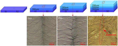
Mosaic diamond: In 1991, first attempts to grow mosaic diamonds have been discussed [Citation43]. The authors used several single crystal diamond seeds, arranged densely in a substrate holder for overgrowth to deposit a large wafer of single crystalline diamond on top. The generation of inch-sized wafers from this technique, however, was delayed until 2014 due to difficulties in connecting single seeds properly [Citation44]. Then, Yamada and co-workers reported for the first time on the synthesizes of a mosaic diamond wafer with 40 mm × 60 mm dimensions. This wafer consisted of 24 single-crystal diamond plates, each 10 mm × 10 mm, grown by microwave plasma chemical vapor deposition. The initial layers showed sometimes cracking and non-uniformity which could be resolved by improved arrangement of crystallographic directions. The mosaic layer technology has been developed to a commercial level by Excellent Diamond Products (EDP) [Citation45], founded in 2009. EDP sells layers of up to 25 mm × 25 mm size. shows the evolution of a junction as function of overgrowth. If seeds are properly arranged, the junction of the substrates connects smoothly [Citation46]. The authors report about Raman mapping which shows that there is a mixture of tensile and compressive stress near the junction.
Hetero-epitaxial growth of diamond: Learning from other semiconductors, heteroepitaxial growth of diamond appears a logical way to grow large diamond wafers. To find a suitable substrate combination for the heteroepitaxial growth of diamond dominated the early research activities. In 1996, Ohtsuka et al. [Citation47] reported for the first time on a successfully fabricated heteroepitaxial diamond layer grown on a Ir(001)/MgO(001) substrate. Since then the heteroepitaxial growth technology for size enlargement of diamond has been developed stage by stage. Crystalline Iridium (Ir) has a face-centered cubic lattice with a lattice constant of 3.84 Å. This is 7.65% higher than the diamond lattice parameter of 3.567 Å [Citation48]. The deposition of cubic single crystal Iridium is challenging as it requires complex substrate combinations. Single-crystal iridium films can be grown on a variety of oxides like Al2O3, SrTiO3 and MgO [Citation49]. The adhesion of diamond/Ir layers on these oxides turned out as major problem, due to large misfits in thermal expansion coefficients. Bauer and coworkers [Citation50] calculated in 2005 the thermal stress developing after cooldown from a deposition temperature of 700 °C assuming a thin diamond film with an iridium buffer layer on top of a thick oxide substrate crystal. They revealed compressive stress values of –4.05 GPa on Al2O3, –6.44 GPa on SrTiO3 and –8.3 GPa on MgO. Silicon shows the smallest stress with –0.68 GPa. In addition, Yttria-Stabilized-Zirconia (YSZ) films turned out as best layer to deposit single-crystalline (100) oriented Ir buffer layers, resulting in a promising hetero-epitaxial film combination: Silicon/YSZ/Ir/diamond.
Figure 2. Growth of mosaic diamond as imaged for 3 overgrowth steps. The boundaries between seeds disappear with increasing thickness. By optimized arrangement of seeds, strain around the boundary can be minimized (From: “Evolution of growth characteristics around the junction in the mosaic diamond”, by X. Zhu et al. 2021, Diamond and Rel. Materials 120 (2021) p. 108640 (Reprinted with permission of Elsevier).
Although these heteroepitaxial grown diamond layers have been improved continuously over recent years (see for a review [Citation51]), their crystalline quality remained defective. The density of dislocations is typically ∼107 to 108 cm−2 which is 8 orders of magnitude higher than optimized HPHT growth [Citation21]. Nonetheless, the wafer diameter of heteroepi-diamond developed accordingly to other semiconductor wafer as shown in [Citation52]. Main drivers behind this developments are (a) Audiatec (since 2015), (b) ShinEtsu (since 2015), (c) AdamantNamiki (since 2020) and (d) DiamondFoundry (since 2022).
Figure 3. The variation of wafer dimensions as function of time for different semiconductor materials. While single crystalline diamond from HPHT (SCD, blue) is enlarging very slowly over time, the enlargement based on mosaic- and hetero-epitaxial growth (HSCD, red) is rapidly progressing and comparable to the developments of the other wafer materials [Citation52].
![Figure 3. The variation of wafer dimensions as function of time for different semiconductor materials. While single crystalline diamond from HPHT (SCD, blue) is enlarging very slowly over time, the enlargement based on mosaic- and hetero-epitaxial growth (HSCD, red) is rapidly progressing and comparable to the developments of the other wafer materials [Citation52].](/cms/asset/9d18135d-15a3-45f6-8cc8-c69628b645fc/tfdi_a_2201592_f0003_c.jpg)
2.4. Dislocation density reduction
Dislocation densities of (107–108) cm−2 are too high for most applications of hetero-epi diamond in electronic devices. Compared to HPHT diamonds, where Sumiya [Citation53] reported already in 1997 dislocation free diamond, significant improvements had to be achieved. A significant breakthrough on dislocation reduction on hetero-epi diamond or diamond in general has been reported in 2018 by Ohmagari and co-workers [Citation54]. They reported a large reduction in threading dislocations from 2 × 10⁶ to 3 × 104 cm−2 by use of Tungsten (W) addition to the growth gas in a hot filament CVD process. In 2022, a first paper on dislocation reduction using microwave assisted CVD deposition was published by Wang et al. [Citation55], again Tungsten (W) was added to the growth gas of the CVD reaction (for example hexacarbonyl (W(CO)6)). Tungsten atoms cause a relaxation of the lattice mismatch at dislocations, inhibiting the propagation of dislocations. The dislocation densities in this microwave CVD process was reduced by two orders of magnitude from 2.8 × 105 cm−2 to 2.5 × 103 cm−2. This is shown schematically in .
Figure 4. Dislocation densities in diamond rang from ca. (107–109)/cm2 in hetero-epitaxial diamond material [Citation51] to nearly zero in HPHT grown IIa diamonds [Citation21]. In 2018 and 2022 a dislocation reduction by Tungsten (W) addition to the growth gas of CVD diamond has been demonstrated by Ohmagari et al. [Citation54] and Wang et al. [Citation55].
![Figure 4. Dislocation densities in diamond rang from ca. (107–109)/cm2 in hetero-epitaxial diamond material [Citation51] to nearly zero in HPHT grown IIa diamonds [Citation21]. In 2018 and 2022 a dislocation reduction by Tungsten (W) addition to the growth gas of CVD diamond has been demonstrated by Ohmagari et al. [Citation54] and Wang et al. [Citation55].](/cms/asset/aa70f925-4847-4a53-ade5-3ea0433be804/tfdi_a_2201592_f0004_c.jpg)
These results are milestones, indicating a major breakthrough with respect to optimization of diamond quality and dislocation minimization. In combination with hetero-epitaxial growth of diamond, it paves the way toward high quality diamond wafer production—a key pre-request for diamond applications in technologies like power electronics and quantum applications.
2.5. Green diamond
Green diamond does not refer to the color of diamond, but to the process and chemicals applied to grow the diamond. If the electric power applied is generated by renewable energy sources like water, solar or wind and the growth gas mixture of methane and hydrogen is not adding CO2 to the atmosphere, the label “green” can be used for CVD diamonds.
The electric power to grow man made diamond can be selected from a manifold of options—including renewable sources. Methane (CH4) and hydrogen (H2), both key ingredients to grow CVD diamond, is mostly ordered from companies which may use natural gas for methane production. Methane is the primary component (90%) of natural gas that is not only an important energy source but also a valuable feedstock for the chemical industry. Methane, if burned, forms CO2, but CO2 can also be used the product methane in a back conversion process (“Sabatier process”). It is a catalytic driven conversion of carbon dioxide (CO2) into methane and well known 1897 [Citation56]. The Sabatier reaction is attracting much attention, because it provides a recycling recipe of CO2 back into fuel. Green hydrogen is also required to grow diamond, which can be generated electrochemically by water splitting using “green electric power”. H2 together with CO2 forms methane, thereby removing CO2 from our atmosphere:
(heat)
(heat)
This reaction is exothermic and releases –164 kJ/mol energy.
Currently; most of hydrogen produced worldwide is made by reforming methane, resulting in CO2 emission of about 830 million tons per year, and which is the other direction of the Sabatier reaction. Water electrolysis is the alternative technology working with 80% efficiency [Citation57]. The electrochemical hydrogen generation is given by:
where a total of at least 285.8 kJ/mol of electric energy and heat is required. Taking into account the efficiency of this process (80%) a total energy of 357.25 kJ/mol is required [Citation58].
In our atmosphere CO2 is present with about 419.84 ppm [Citation59]. Direct air capture (DAC) technologies to extract CO2 from the atmosphere are currently hot topics. Unfortunately, these DAC technologies are energy demanding with typical (308–440) kJ/mol [Citation60], a technique which therefore needs further improvements. Better would be capturing at point sources like carbon power stations or cement plants.
The total energy required for methanization of CO2 from the atmosphere is therefore in the range 665–800 kJ/mol (CO2 capture plus water electrolysis). Compared to the use of natural gas and the reforming of methane (generation CO2) it is a truly environmentally sound approach. Although this green CO2 to CH4 reaction requires energy, the excess energy production of solar and wind power plants at times of no or little demand, makes this technology attractive and suitable.
2.6. The energy efforts
To evaluate the energy consumptions of various diamond production technologies Zhdanov and co-workers published in 2021 [Citation61] a comparative study comparing (a) natural, (b) HPHT and (c) microwave CVD diamond production. Publicly available reports issued by DeBeers and ALROSA are used to estimate the energy/carat (1 ct = 0.2 g) efforts of natural rough diamonds (including all energy required to mine) which is 150 kWh/ct for DeBeers and 96 kWh/ct for ALROSA. These values are comparted with energy costs for producing diamonds by High-Pressure-High-Temperature (HPHT) and microwave-assisted Chemical Vapor Deposition (MCVD). The authors introduce for a state-of the art HPHT process, with open cooling circuits, about 36 kWh/ct when producing gem-quality and average-sized (near-) colorless diamonds. The energy consumption of MCVD processes can be different and depend on (a) type of MCVD-reactor, (b) microwave frequency (2.45 GHz or 915 MW), (c) single or multi-seed growth, (d) growth speed (gas mixtures and pressure), etc. and range therefore between 77 kW/ct for data from IIa Technology and 143 kW/ct for data from Ekati. The corresponding energy required to produce wafer-grade Silicon [Citation62] is 0.425 kWh/ct. summarizes these data.
Table 2. Energy per carat require to produce diamond and compared to Si.
This comparison reveals a major problem of diamond technology. The energy consumption for HPHT diamonds is currently 66–85 times higher than for Silicon. For MCVD it is even worse, namely 181–337 times. The accuracy of these numbers may vary within limits, but the result show that the manufacturing of diamond needs to be significantly improved to become a serious competitor to silicon.
One of the reasons for this mis-proportion is the sophisticated technology which is required for HPHT growth, the other is the outdated microwave technology needed for microwave based deposition. Applied microwave deposition is still based on developments started in 1983 [Citation19] by the famous NIRIM reactor.
The microwave is emitted into a metal confinement which generates a resonator field which is dependent on the geometry of the metal confinement and the used microwave frequency (or better wavelength). The microwave energy is translated into hydrogen/methane plasma with a fixed shape and dimension which also dependent on the applied pressure. During the last 30 years only little has been changed. In 1996 the ASTEX reactor type [Citation63] and later in 1999 the ellipsoid reactor [Citation64] were established. The source of energy is a magnetron working at 2.45 GHz or 915 MHz, emitting 6–12 kW power. For larger reactors, magnetron with up to 60 kW are commercially available. Magnetron tubes are well established, however, they show a limited lifetime of a few thousand hours (2000 h up to 8000 h) depending on the tube. They are difficult to troubleshoot and service, which results in costly downtime and repairs.
During recent years, solid state microwave systems have been developed and become increasingly implemented into microwave CVD technologies. They appear robust with a lifetime of more than 500,000 h. The long term total cost therefore can be significantly reduced. The energy spectrum of the MW emission is narrow, several emitters can be combined and phase-locked. If multi-antenna emitters are used the emission can be rotated to homogenize the plasma, to rotation it or to move the plasma over larger areas. The emission can be pulsed or continuous. Large area microwave diamond deposition will become available [Citation65]. Altogether, a major innovation step which comes timely and may cause a significant cost reduction of diamond production.
3. Summary and conclusions
CVD diamond materials and GEMs are on the move and diamond will become a global and big player. In 2021, the global market of synthetic diamond (HPHT and CVD) was in the range of 14 billion USD, growing with 8%. About 40% was attributed to HPHT and 60% to CVD (polished and rough) [Citation66]. This can be compared to the global diamond jewelry market of 65–80 billion USD. For comparison, the global SiC market in 2021 was ca. 3 billion USD (CAGR 11.7%) [Citation67] and the global GaN semiconductor device market was 1.88 billion USD in 2021 (CAGR 24.4) [Citation68].
These numbers demonstrate the importance of diamond technology. The research and developments in the future need roadmaps to tune the science and development progress of the related development of equipments. To produce diamond material in wafer scale dimensions (2–4 inch or larger), new deposition systems need and will be used in combination with related etching-, photolithography, stepper and metallization techniques. The in-time developments require intense planning and communication.
CVD diamond technology is well progressing. A key and major step will be the diamond wafer production with electronic quality. Here, recent dislocation density minimization took an important step, the control of defects as well as of purity seems to be established. Several companies are currently establishing large area diamond production on the basis of mosaic diamond or on hetero-epitaxial technology. Applications in MEMS or as heat-spreaders are not really demanding with respect to defects. They can be to “door opener” for the start of wafer production with limited electronic and optical quality. As time goes by an improvement in quality as well as in wafer size will be mandatory.
Device prototypes in quantum technology, power electronics, electro -and bio-electrochemistry, MEMS and radiation detection have been realized. Most of the developments achieved “prototype” level or TLR 4, which is a result of the missing wafer. To establish collaborations with companies, the prototype device needs to show potential for mass production. A demanding requirement as (a) diamond wafers need to be available as well as (b) markets. Based on data available in the literature, the market expectations can be summarized as follows:
The global magnetometry market for NV centers in diamond in 2023 will approach 160 M USD (with CAGR of 7.9%) [Citation69].
The market for man made diamond nano-particles will reach 140 M USD in 2025 (CAGR = 12.4.%) [Citation70].
The power electronic market for diodes >3 kV is in the range of 35 M USD in 2023 [Citation71].
These markets can be addressed by diamond devices, if diamond wafers are available in time.
New applications with large markets are heat spreaders (32 M USD in 2020 [Citation71]) and MEMS (1150 M USD in 2019 [Citation70]), both markets are demanding. MEMS on the basis of AlScN/diamond and heat spreader for 5G amplification stations based on GaN/diamond suffer from the enormous misfit of thermal expansion coefficients and are therefore difficult to combine. New techniques like wafer-bonding can be a solution to this problem. Besides, certain applications require 8 inch or larger wafers for commercialization and combination with other materials like AlScN. In addition, these devices especially filters in 5G communication devices like cellular phones need to be cheap. Finally, quantum applications of diamond are very attractive and show the biggest global market. Diamond is unique in this field but mass production will be required to access and penetrate such markets [Citation72].
In summary, the CVD diamond technology is well progressing with respect to diamond quality, doping, 3D shaping, wafers production and optimization and device prototyping. Markets for diamond applications are defined and promising. Required key improvements are (a) cost reduction in diamond deposition technology as well as (b) the establishment of diamond wafers for mass production. Both topics are addressed by the diamond community and will be the bottle neck for success in the future.
Acknowledgement
The author thanks Norio Tokuda, and Satoshi Yamasaki, Kanazawa University, Japan, for their support and continuous discussions on diamond related topics.
Disclosure statement
No potential conflict of interest was reported by the author.
References
- Kamina S. Trillion sensors and MEMS. Sensors Mater. 2018; 30(4): 723–773.
- Yole. Emerging semiconductor substrates. Lyon, France: YOLE INTELLIGENCE; 2019.
- Lee K-W. 3-D hetero-integration technologies for multifunctional convergence systems. J Microelectron Packag Soc. 2015;22(2):11–19.
- Sang L. Diamond as the heat spreader for the thermal dissipation of GaN-based electronic devices. Funct Diamond. 2021;1(1):174–188.
- Nebel CE, Aharonovich I, Mizuochi N, et al. editors. Diamond for quantum applications part 1. Semiconductors and semimetals 103. London: Elsevier; 2020. ISBN 978-0-12-820240-1.
- Nebel CE, Aharonovich I, Mizuochi N, et al. editors. Diamond for quantum applications part 2. Semiconductors and semimetals 104. London: Elsevier; 2021. ISBN 978-0-323-85024-7.
- Brillas E, Martinez-Huitle CA, editors. Synthetic diamond films, preparation, electrochemistry, characterization and applications. Wiley Series on Electrocatalysis and Electrochemistry, John Wiley & Sons. 2011. ISBN 978-1-118-06236-4.
- Parangi T. A review on electrochemical and photochemical processes for hydrogen production. Comments Inorg Chem. 2022; 42(5): 271–336.
- REACH: Registration, Evaluation, Authorization and Restriction of Chemicals: see : https://en.wikipedia.org/wiki/Registration,_Evaluation,_Authorisation_ad_Restriction_of_Chemicals.
- Gogotsi Y, Presser V, editors. Carbon nanomaterials. CRC Press; 2021. ISBN 9781138076815.
- Sarin VK, Nebel CE, editors. Comprehensive hard materials, super hard materials. Vol. 3, London: Elsevier; 2014. ISBN 978-0-444-63383-5.
- Bragg WH, Bragg WL. The structure of the diamond. Proc R Soc. 1913;156(610):277–291.
- Raman CV. Allotropic modifications of diamond. Nature. 1945;156(3949):22–23.
- Bundy FP, Hall HT, Strong HM, et al. Man-made diamonds. Nature. 1955;176(4471):51–55.
- Eversole WG. Synthesis of diamond, US patents 3,030,187,3,030,188, filed July 23, 1958.
- Angus JC, Will HA, Stanko WS. Growth of diamond seed crystals by vapor deposition. J Appl Phys. 1968;39(6):2915–2922.
- Spitsyn BV, Deryagin BV. A technique of diamond growth on a diamond face, USSR Inventor’s Certificate 339,134 filed in July 10, 1956, published in a Bulletin of Inventions No 17; 1980, p. 323.
- Matsumoto S, Sato Y, Tsutsumi M, et al. Growth of diamond particles from methane-hydrogen gas. J Mater Sci. 1982;17(11):3106–3112.
- Kamo M, Sato Y, Matsumoto S, et al. Diamond synthesis from gas in microwave plasma. J Cryst Growth. 1983;62(3):642–644.
- Angus JC. Diamond synthesis by chemical vapor deposition: the early years. Diamond Relat Mater. 2014;49:77–86.
- Sumiya H, Tamasaku K. Large defect-free synthetic type IIa diamond crystals synthesized via high pressure and high temperature. Jpn J Appl Phys. 2012;51(9R):090102.
- Kato H. Conductivity and impurity doping on single crystal diamond. In: Sarin VK, Nebel CE, editors. Comprehensive hard materials, super hard materials. Vol. 3, London: Elsevier; 2014, pp. 305–319. ISBN 9780-444-63383-5.
- Araujo D, Suzuki M, Lloret F, et al. Diamond for electronics: materials, processing and devices. Materials. 2021;14(22):7081.
- Nebel CE. General properties of diamond. In: Arnault J-C, editors, Nanodiamonds, advanced material analysis, properties and applications, London: Elsevier; 2017. pp. 1–24. ISBN 9780-323-43029-6.
- Mildren RP. Intrinsic optical properties of diamond. In: Mildren RP, Rabeau JR, editors, Optical engineering of diamond, Wiley-VCH; 2013. pp. 1–34. ISBN 9783527411023.
- Gruber A, Dräbenstedt A, Tietz C, et al. Scanning confocal optical microscopy and magnetic resonance on single defect centers. Science. 1997;276(5321):2012–2014.
- Yamasaki S, Makino T, Takeuchi D, et al. Potential of diamond power devices. In: Proceedings of the 25th International Symposium on Power Semiconductor Devices & ICs, Kanazawa, 6.2; 2013, pp. 307–310.
- Iwaki M, Sato S, Takahashi K, et al. Electrical-conductivity of nitrogen and argon implanted diamond. Nucl Instrum Methods Phys Res. 1983;209–210:1129–1133.
- Angus JC. Electrochemsitry on diamond: history and current status. In: Brillas E, Martinez-Huitle CA, editors, Synthetic diamond films, preparation, electrochemistry, characterization and applications, John Wiley&Sons; 2011, pp. 3–20. ISBN 9781-118-06236-4.
- Nebel CE. Surface electronic properties of diamond. In: Sarin VK, Nebel CE, editors, Comprehensive hard materials, super hard materials, Vol. 3, London: Elsevier; 2014, pp. 339–364. ISBN 9780-444-63383-5.
- Salvadori MC, Araújo WWR, Teixeira FS, et al. Termination of diamond surfaces with hydrogen, oxygen and fluorine using a small, simple plasma gun. Diamond Relat Mater. 2010;19(4):324–328.
- Widmann CJ, Giese C, Wolfer M, et al. F- and Cl-terminations of (100) oriented single crystalline diamond. Phys Status Solidi A. 2014;211(10):2328–2332.
- Maier F, Ristein J, Ley L. Electron affinity of plasma-hydrogenated and chemically oxidized diamond (100) surfaces. Phys Rev B. 2001;64(16):165411.
- Cui JB, Ristein J, Ley L. Electron affinity of the bare and hydrogen covered single crystal diamond (111) surface. Phys Rev Lett. 1998;81(2):429–432.
- Zhu D, Zhang LH, Ruther RE, et al. Photo-illuminated diamond as a solid-state source of solvated electrons in water for nitrogen reduction. Nat Mater. 2013;12(9):836–841.
- Maier F, Riedel M, Mantel B, et al. Origin of surface conductivity in diamond. Phys Rev Lett. 2000;85(16):3472–3475.
- Sumiya H. HPHT synthesis of large, high quality single crystal diamond. In: Nebel CE, editors, Comprehensive hard materials, Vol. 3, London: Elsevier; 2014, pp. 109–215. ISBN 9780-444-63383-5.
- Sumiya H, Satoh S. High-pressure synthesis of high-purity diamond crystal. Diamond Relat Mater. 1996;5(11):1359–1365.
- Mokuno Y, Chayahara A, Soda Y, et al. Synthesizing single-crystal diamond by repetition of high rate homoepitaxial growth by microwave plasma CVD. Diamond Relat Mater. 2005;14(11–12):1743–1746.
- Chayahara A, Mokuno Y, Horino Y, et al. The effect of nitrogen addition during high-rate homoepitaxial growth of diamond by microwave plasma CVD. Diamond Relat Mater. 2004;13(11–12):1954–1958.
- Silva F, Achard J, Brinza O, et al. High quality, large surface area, homoepitaxial MPACVD diamond growth. Diamond Relat Mater. 2009;18(5–8):683–697.
- Gicquel A, Silva F, Hassouni K. Diamond growth mechanisms in various environments. J Electrochem Soc. 2000;147(6):2218.
- Geis MW, Smith HI, Argoitia A, et al. Large-area mosaic diamond films approaching single-crystal quality. Appl Phys Lett. 1991;58(22):2485–2487.
- Yamada H, Chayahara A, Mokuno Y, et al. A 2-in. mosaic wafer made of a single-crystal diamond. Appl Phys Lett. 2014;104(10):102110.
- https://www.d-edp.jp/en/.
- Zhu X, Liu J, Shao S, et al. Evolution of growth characteristics around the junction in the mosaic diamond. Diamond Relat Mater. 2021;120:108640.
- Ohtsuka K, Suzuki K, Atsuhito Sawabe AS, et al. Epitaxial growth of diamond on iridium. Jpn J Appl Phys. 1996;35(8B):L1072.
- Gsell S, Bauer T, Goldfuß J, et al. A route to diamond wafers by epitaxial deposition on silicon via iridium/yttria-stabilized zirconia buffer layers. Appl Phys Lett. 2004;84(22):4541–4543.
- Fischer M, Gsell S, Schreck M, et al. Preparation of 4-inch Ir/YSZ/Si(001) substrates for the large-area deposition of single-crystal diamond. Diamond Relat Mater. 2008;17(7–10):1035–1038.
- Bauer T, Gsell S, Schreck M, et al. Growth of epitaxial diamond on silicon via iridium/SrTiO3 buffer layers. Diamond Relat Mater. 2005;14(3–7):314–317.
- Schreck M. in, Vol Single crystal diamond growth on iridium. In: Nebel CE, editors, Comprehensive hard materials. Vol. 3, Elsevier; 2014, pp. 269–304. ISBN 9780-444-63383-5.
- Yole Development. Emerging semiconductor substrates: market and Technology Trends; Lyon, France: YOLE INTELLIGENCE; 2019.
- Sumiya H, Toda N, Nishibayashi Y, et al. Crystalline perfection of high purity synthetic diamond crystal. J Crystal Growth. 1997;178(4):485–494.
- Ohmagari S, Yamada H, Tsubouchi N, et al. Large reduction of threading dislocations in diamond by hot-filament chemical vapor deposition accompanying W incorporations. Appl Phys Lett. 2018;113(3):032108.
- Wang R, Lin F, Niu G, et al. Reducing threading dislocations of single-crystal diamond via in situ tungsten incorporation. Materials. 2022;15(2):444.
- Rönsch S, Schneider J, Matthischke S, et al. Review on methanation – from fundamentals to current projects. Fuel. 2016;166:276–296.
- https://www.thyssenkrupp.com/de/unternehmen/innovation/technologien-fuer-die-energiewende/wasserelektrolyse.html.
- Idriss H. Hydrogen production from water: past and present. Curr Opin Chem Eng. 2020;29:74–82.
- https://www.co2.earth/daily-co2#:∼:text=418.60%20ppm&text=This%20table%20presents%20the%20most,atmospheric%20CO2%20on%20the%20planet.
- https://www.iea.org/reports/direct-air-capture.
- Zhdanov V, Sokolova M, Smirnov P, et al. A comparative analysis of energy and water consumption of mined versus synthetic diamonds. Energies. 2021;14(21):7062.
- Krishnan N, Boyd S, Somani A, et al. A hybride life cycle inventory of nano-scale semiconductor manufacturing. Environ Sci Technol. 2008;42(8):3069–3075.
- Besen MM, Sevillano E, Smith DK. Microwave plasma reactor. Applied Science and Technology, United States Patent 5,556,475, Sep. 17, 1996.
- Füner M, Wild C, Koidl P. Simulation and development of optimized microwave plasma reactors for diamond deposition. Surf Coat Technol. 1999;116–119:853–862.
- Du ZL, Wu Z, Gan WW, et al. Multi-physics modeling and process simulation for a frequency-shifted solid-state source microwave oven. IEEE Access. 2019;7:184726–184733.
- https://www.mordorintelligence.com/industry-reports/synthetic-diamond-market.
- https://www.grandviewresearch.com/industry-analysis/silicon-carbide-market.
- https://www.grandviewresearch.com/industry-analysis/gan-gallium-nitride-semiconductor-devices-market.
- https://www.transparencymarketresearch.com/magnetometer-sensor-market.html.
- https://www.adroitmarketresearch.com/industry-reports/nanodiamond-market.
- Yole. Diamond Materials for Semiconductor Applications; 2013.
- Yole. AlScN-MEMS-filter for high-frequency-communication: markets and properties; 2014.