
 ?Mathematical formulae have been encoded as MathML and are displayed in this HTML version using MathJax in order to improve their display. Uncheck the box to turn MathJax off. This feature requires Javascript. Click on a formula to zoom.
Abstract
A resonator with a high Q factor is generally pursued in the single-crystal diamond (SCD) microelectromechanical system (MEMS) for high-performance sensors. In this report, we investigate the oxygen etching effect of SCD on the Q factors of the SCD resonators by using the Raman spectroscopy spatial mapping. We aim to establish the etch pit effect on the Q factors of the SCD MEMS resonators. The 2D Raman imaging technique discloses the dislocations and the local stress in the SCD MEMS resonators in microscale. It is observed that the full width half maximum (FWHM) of the Raman spectra of the SCD resonators has marked relationship with the Q factors of the SCD resonators. The etch pits resulted from the dislocations have weak influence on the Q factors of the SCD resonators.
1. Introduction
Single-crystal diamond (SCD) is a promising material for microelectromechanical system (MEMS) techniques by virtue of its superior electronic properties, outstanding mechanical properties, the highest thermal conductivity, and chemical inertness [Citation1–5]. SCD MEMS resonators have potential applications in various fields ranging from physical and chemical sensors to biological disease diagnosis [Citation2, Citation6]. The quality (Q) factor, a key figure of merit of a MEMS resonator, is defined as the ratio of the measure of energy loss per oscillation to the total energy of the resonator [Citation7]. High Q factor is generally desirable, which makes a device more efficient, less susceptible to mechanical noise [Citation8], more sensitive to the minimum detectable force [Citation4, Citation9] and highly stable to harsh conditions [Citation10, Citation11]. For a SCD MEMS resonator, the Q factor is determined by the multiple dissipation mechanisms [Citation7, Citation12]. Particularly, the bulk defects effect, dominated by the SCD crystal quality and defects, has a critical impact on the Q factor [Citation13].
The crystal qualities of the homoepitaxial SCD films, grown on the SCD substrates by using the chemical vapor deposition (CVD) technique, depend on the growth conditions and the substrate quality [Citation14, Citation15]. Nowadays, impurities incorporation such as nitrogen or boron is well controlled, while the dislocations are still inevitable in the CVD SCD epilayers [Citation15, Citation16]. These dislocations defects stem from (i) the dislocations induced by the substrate surface state and the mechanical polishing and (ii) the growth dislocations from defects in the substrate such as stacking faults. The dislocation density robustly affects the crystal quality and hence the performance of the SCD MEMS resonators. Having a better understanding of the relationship between the dislocation and the Q factor is in favor of developing high-Q factor SCD resonators.
Recently, many efforts had been devoted to developing high Q factors of the SCD resonators via the fabrication method [Citation4, Citation17] and the slow chemical etching [Citation13]. The diamond-on-insulator (DOI) method was proposed to achieve high Q factors for the SCD resonators. A smart-cut method was developed to achieved SCD-on-SCD MEMS resonators based on the ion implantation [Citation3, Citation12, Citation18, Citation19]. By using oxygen etching to remove the ion-implantation induced defects, the Q factor was effectively improved over 1 million [Citation13, Citation20]. However, the oxygen etching also induced the etch pits on the SCD MEMS resonators due to the existence of dislocations. The effect of the local dislocations on the Q factors of the SCD resonators need to be clarified to further improve the Q factors.
In this work, we analyzed the crystal quality effect on the Q factor of the SCD MEMS resonators by using the 2D Raman spectroscopy technique. The precise dislocation positions and the dislocation-induced local stress of the SCD epilayer were visualized through the 2D Raman imaging technique. Through the SCD MEMS resonators, the dependence of the full width half maximum (FWHM) of the Raman spectra on the Q factors was disclosed, indicating a low FWHM resulted in achieving high Q factor. To some extent, the numbers of the etch pits resulted from the dislocations have tiny impact on the Q factors.
2. Experimental
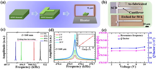
A high-pressure and high-temperature (HPHT) type-I b (100) SCD substrate was utilized to grow the homoepitaxial SCD film via a microwave plasma CVD (MPCVD, SEKI TECHNOLOGY, AX2115) system. The SCD substrate was processed by the ion implantation and cleaned in a boiling mixture-acid of H2SO4 and HNO3 before the CVD growth. The growth parameters of the MPCVD for the SCD epilayer were: a CH4 flow of 10 sccm, a H2 flow of 500 sccm, a chamber pressure of 80 Torr, a microwave power of 1000 W, a substrate temperature around 950 °C, and a growth duration of 1 h. After the CVD epilayer growth, the as-grown SCD sample was utilized to produce the SCD MEMS cantilevers. The fabricated method was described in details in our previous works [Citation3, Citation12, Citation18, Citation19]. The fabrication process of the SCD MEMS cantilevers is described in Figure S1 (Supporting Information). Then, the as-fabricated SCD sample with cantilevers was annealed at 650 °C for 20 hrs, 20 hrs, and 10 hrs (totally 50 hrs) in a tube furnace with an oxygen ambient.
The surface morphologies of the SCD sample were investigated by using an atom force microscopy (AFM, Bruker). The 3D profiles of SCD cantilevers were examined by using a 3D laser optical microscopy (VK-9710). The crystal quality of the SCD sample was examined by a confocal Raman system (WITec α-300r). The wavelength and power of the excitation laser were 532 nm and 20 mW, respectively. The spectrometer was equipped with a 1800 Lmm−1 monochromator grating and a cooled charge-coupled device detector. In order to achieve a 2D Raman image with high resolution, the lateral (X-Y plane) and the vertical (X-Z plane) spatial resolutions were set to be 0.4 μm and 0.1 μm, respectively, during the measurement. All measurements were performed at room temperature. The mechanical resonance performances of the SCD cantilevers without and with the etching treatment were measured by the optical readout system with the Laser Doppler Vibrometry (LV 1710) system. The resonance performance tests were performed in a vacuum chamber with a pressure less than 10−3 Pa. A micro-probe placed above these SCD cantilevers, was connected to a RF signal to actuate the resonance vibration. A lock-in amplifier system was utilized to read out the optical signals of the SCD cantilevers due to their harmonic vibrations.
3. Results and discussion
In the smart-cut method, a non-diamond layer, resulted from the ion-implantation treatment, inevitably exists in the as-fabricated SCD cantilevers, which is detrimental to the Q factors. The oxygen etching offers a promising strategy to remove the surface layers (the defective-diamond layer and the diamond layer) and other defects, which exhibit the great influence on the Q factors of the SCD cantilevers [Citation14, Citation21, Citation22]. The etching mechanism of the SCD in an oxygen ambient is described in detail in Figure S2. shows the schematic diagram of the etching treatment process for the SCD cantilevers. The oxygen etching for the SCD sample was carried out in the tube furnace. The etch pits appear on the SCD cantilever due to the oxygen etching treatment, as indicated in . For a rectangle mechanical resonator, the harmonic vibration characteristics were expressed by the Euler-Bernoulli beam theory [Citation2, Citation18, Citation23]. The resonance frequency is expressed as,
(1)
(1)
where k is 0.162 for the first vibration mode of the resonator. t and L are the thickness and the width of the resonator, respectively. E is the Young’s modulus and ρ is the mass density of materials. For the resonator with the multilayers, the Young’s modulus and the mass density are defined as the effective Young’s modulus and the effective mass density, respectively. The parameters utilized in EquationEq. (1)
(1)
(1) are the dimensions and material properties, which depend on the resonator material. The resonance frequency spectrum shifts downward with the etching duration increasing, as shown in . shows the resonance frequency spectra of the resonators after the etching treatment for 20 hrs as a function of the RF actuation amplitude. The peak amplitudes of resonance spectra linearly increase with the driving voltages (the inset of ). The dependences of the resonance frequencies and Q factors on the driving voltages are exhibited in , indicating the driving voltage has little impact on the resonance frequencies and the Q factors of the SCD cantilevers.
Figure 1. (a) The simplified treatment process for the chemical etching of the SCD cantilevers in an oxygen ambient. (b) Optical images of a 160 um-long SCD cantilever without and with the etching treatment. (c) Resonance spectra shifts of the SCD cantilever with the etching duration increasing. (d) The typical resonance frequency spectra of a 160 μm-long SCD cantilever suffered from the oxygen etching for 20 hrs. The inset shows that the peak amplitude linearly increases with the actuation voltage. (e) Resonance frequencies and Q factors as a function of the actuation voltages.
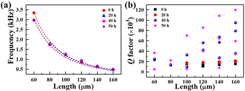
The dependences of the resonance frequencies on the lengths of the SCD cantilevers after the etching treatments with various durations are depicted in . The rule of resonance frequencies and lengths of these cantilevers strictly follows the law of EquationEq. (1)(1)
(1) . The etching treatment leads to the reduction in the resonance frequencies of the SCD cantilevers due to the reduction of the thickness (Figure S3). The reduced thicknesses of the SCD cantilevers due to the etching treatment can be calculated through the EquationEq. (1)
(1)
(1) . In views of the both sides for a SCD cantilever, the average etching rate of the SCD cantilevers is evaluated as 2.2 nm/h at 650 °C. This etching rate in the pure oxygen ambient make it a difficulty in measuring the accurate etching value by using the traditional methods, such as the step height profiler [Citation24] and the low-coherence interferometry technique [Citation25]. shows the variations of Q factors of the SCD cantilevers under the etching treatments with various etching durations. It can be seen that the Q factors of the SCD cantilevers increase with the etching durations as the etching durations lower than 40 hrs. The Q factors of some SCD cantilevers appear to decrease with the etching durations extending to 50 hrs. For a cantilever beam, the Q factor was significantly determined by the various energy dissipations [Citation12]. In this work, the SCD cantilevers were fabricated by the smart-cut method. The smart-cut method produces an ion-implantation damaged layer, which is defective and degrades the Q factors of the as-fabricated SCD cantilevers. A bilayer model was proposed to describe the impact of the ion-implantation damaged layer on the Q factors of SCD cantilevers consisting of a damaged layer and a high-quality homoepitaxial layer [Citation26],
(2)
(2)
wherein Q is the quality factor of the overall cantilever. Qepi represents the quality factor of the epilayer. Qion is the quality factor of the ion-implantation damaged layer. β is defined as β = Eiontion/Eepitepi. Eion and Eepi are the Young’s modulus of the ion-damaged layer and the epilayer, respectively. tion and tepi are the thicknesses of the ion-damaged layer and the epilayer, respectively. When Eion and Eepi are assumed to be equal, β is simply expressed as tion/tepi. The reduced β indicates the ion-damaged layer is gradually eliminated. The previous research shows that the Qion of the ion-damaged layer alone is generally less than 1000 [Citation18]. The Qepi of the high crystal quality epilayer, which is toward 106, is far larger than the Qion [Citation13]. Thus, the overall Q factor of the SCD cantilever is mainly determined by the ion-damaged layer (defective diamond layer). Through the etching treatment in an oxygen ambient, the surface layers are removed by the oxygen at high temperatures. The structure of the diamond layer is more stable than that of the defective-diamond layer, which leads to a higher etching rate for the defective diamond layer. According to EquationEq. (2)
(2)
(2) , the Q factors of the SCD cantilevers can be greatly enhanced through the reduction of the defective diamond layer. Furthermore, the removal of the dislocations on the SCD epilayer via the oxygen etching also helps to reduce the defects-related energy dissipation, resulting in the increase in Q factor. In , the etching treatment within 40 hrs to 50 hrs leads to the reduction in the Q factors of some SCD cantilevers, which discloses that the ion-damaged layer is completely removed and the etching on the surface has the critical impact on the Q factors during this term. The reduction in the Q factors of some SCD cantilevers after the etching for 50 hrs may be attributed to the damage of the boundary integrity.
Figure 2. Dependences of (a) resonance frequencies and (b) Q factors of the SCD cantilevers under the etching treatment with various durations on the cantilever length L.
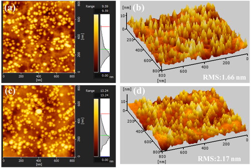
The surface morphologies of the SCD substrate and the SCD epilayer are measured by the AFM technique, as shown in . After the etching treatment, the SCD substrate and the SCD epilayer still exhibit a smooth surface with a tiny root-mean-square (RMS) of roughness lower than 2.2 nm. In addition, for the SCD epilayer, the dislocation density can range from 10 to 107 cm−2, which depends on the crystal quality of the initial substrates, as well as the growth conditions [Citation14, Citation27]. The SCD cantilevers have a few dislocations in view of the cantilever dimensions. The dislocation defects with high energies on the surface of the SCD epilayer are most susceptible to be etch by the oxygen [Citation15, Citation21, Citation22, Citation28]. The etch pits appear on the area with the dislocations after the oxygen etching treatment, as shown in Figure S4. The etch pits resulted from the dislocations exhibit the circle characteristics. The propagation of the oxygen along the dislocations is in favor of the vertical etching of the SCD epilayer, which results in the pits on the surface.
Figure 3. Surface morphologies of (a) and (b) the SCD substrate and (c) and (d) the SCD epilayer after the etching for 50 hrs.
Although the common techniques including x-ray topography (XRT), cathodoluminescence (CL), and birefringence microscopy have been used to investigate the dislocation in CVD diamonds [Citation29–32], the 2D Raman imaging technique makes it possible to accurately evaluate the position and the local strain of a dislocation in the SCD epilayer. The 2D Raman imaging of the SCD was described in detail in previous work [Citation32]. The peak position, Ppeak, was obtained by the Lorentz function fitting of the Raman spectra of each measured point. The FWHM was achieved as a dispersion of the Raman spectra with the Lorentz function. The average Ppeak and the average FWHM were calculated as the Ppeak histogram and FWHM histogram by using Gauss function fitting, respectively.
exhibits the 2D Raman mapping images in the X-Y plane of an area of 50×50 μm2 on the SCD epilayer after the oxygen etching for 50 hrs. The 2D images of the Raman Ppeak and the FWHM of this area are displayed in and (c), respectively. The histograms of the Ppeak and the FWHM are shown in and (d), respectively. The color bars in and (c) represent the value ranges of the Ppeak and the FWHM, respectively. It is shown that there are three dislocations appeared in this area, which are marked by the green arrows in and (c). In order to investigate the difference in Ppeak and the FWHM around a dislocation, the line A-B and the line A′-B′ across the area with one dislocation in and (c), respectively, are marked for the clear view, while the line C-D and the line C′-D′ is for the area without a dislocation, as shown in and (c), respectively. and (g) show the variations of the Ppeak with the distance from A point to B point and the distance from C point to D point, respectively. It is disclosed that there is a large shift in the Ppeak around a dislocation, while the weak difference in the Ppeak appears for the area without a dislocation. The difference in the Ppeak, ΔPpeak, between the measured area and the SCD substrate reveals the internal stress in the measured area. By the assumption of the biaxial stress in the SCD epilayer, the stress, σ was evaluated in the following expression [Citation32, Citation33],
(3)
(3)
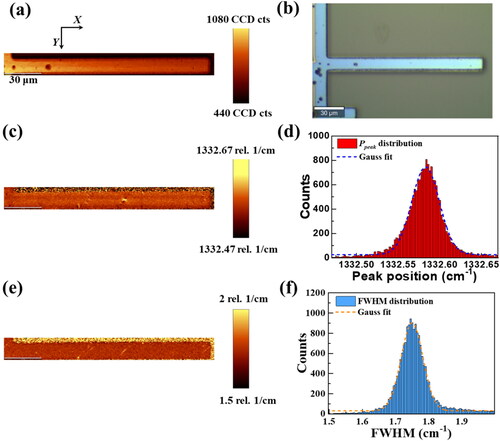
Figure 4. Raman imaging in the X-Y plane of an area of 50×50 µm2 in the SCD epilayer after the etching treatment for 50 h. (a) 2D image of the Raman peak position (Ppeak) distribution of the Raman spectra. Dislocations are marked by the green arrows. The line A-B goes cross the area with one dislocation, while the line C-D goes cross the area without one dislocation. (b) Histogram distribution of Raman Ppeak. (c) 2D image of full width at half maximum (FWHM) distribution of the Raman spectra. Dislocations are also marked by the green arrows. The line A′-B′ goes cross the area with one dislocation, while the line C′-D′ goes cross the area without one dislocation. (e) and (g) Dependences of Ppeak on the distance from A point to B point and the distance from C point to D point, respectively, marked in (a). (f) and (h) Dependences of FWHM on the distance from A′ point to B′ point and the distance from C point to D point, respectively, marked in (b).
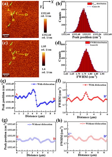
When the SCD epilayer suffers from a compressive stress, σ is positive, while a negative value of σ indicates a tensile stress. In addition, the Ppeak of the SCD substrate is measured as 1332.54 cm−1 (Figure S5). In , it can be obtained that around the dislocation, the largest value of the Ppeak reaches 1332.60 cm−1, while the smallest value of the Ppeak is 1332.46 cm−1. According to EquationEq. (3)(3)
(3) , the largest values of the compressive stress and the tensile stress around the dislocation are calculated to be ∼ −36.6 MPa and ∼48.8 MPa, respectively. The dislocations act as the weakest part to be etched in the oxygen ambient. The dependences of the FWHM on the distance from A′ point to B′ point and the distance from C′ point to D′ point are exhibited in and (h), respectively. It is revealed that the FWHM shows a large increase from 1.76 cm−1 to 1.87 cm−1 around the dislocation along the line A′-B′ point, while the FWHM along the line C′-D′ point without the dislocation is around 1.77 cm−1 with little change. The local area around the dislocation has a higher FWHM, which means a worse crystal quality in this area. Therefore, the 2D Raman imaging technique with the statistic measurements and the data fitting can visualize the precious dislocation position, the dislocation-induced local stress, and the crystal quality variation. The existence of the dislocations on the SCD cantilevers have a negative influence on the crystal qualities, thereby affecting the Q factors.
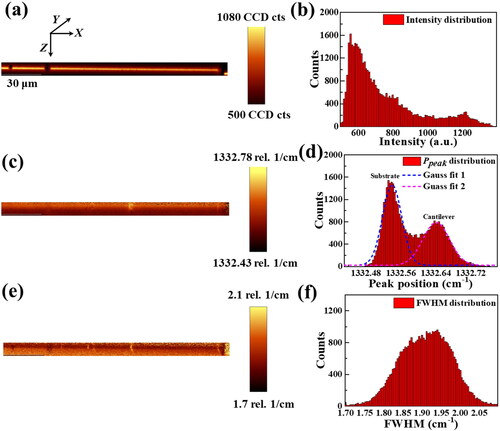
The Raman technique offers a facile and effective method to evaluate the crystal qualities of the substrate and the epilayer. The surface stress of the SCD cantilevers were investigated in our previous work [Citation34], which had little impact on the resonance properties. In this work, the dependence of the Q factor on the crystal quality of the SCD cantilevers after the oxygen etching treatment are observed via the Raman spectroscopy. In order to comprehensively investigate the crystal qualities and the structures of the SCD cantilevers, Raman spectra were measured in the X-Y plane and in the X-Z plane, respectively. The 2D Raman images in the X-Y plane of an area of 170×18 μm2 around the 160 μm-long SCD cantilever after the oxygen etching for 50 hrs are shown in . The image with the Raman peak intensity is exhibited in , showing a cantilever with the etch pits, consistent with the optical image in . The 2D Raman images of the Ppeak distribution and the FWHM distribution of this measured area are displayed in and (e), respectively. The histograms of the Ppeak and the FWHM are shown in and (f), respectively. Although the measured area contains a tiny area of the defective SCD epilayer, the average Ppeak of the measured area are 1332.58 cm−1. The crystal quality of the epilayer can be evaluated by the FWHM of the Raman spectra. In , the average FWHM of the measured area is calculated to be 1.75 cm−1, which is lower than that of the SCD substrate of 1.88 cm−1 (Figure S5).
Figure 5. Raman mapping in the X-Y plane of an area of 170×18 μm2 around the SCD cantilever after the etching treatment for 50 hrs. (a) 2D mapping of Raman peak intensity. (b) Optical image. (c) 2D mapping of the Raman Ppeak. (d) Histogram distribution of Raman Ppeak. (e) 2D mapping of FWHM. (f) Histogram distribution of FWHM.
In order to obtain the cross-section view of the SCD cantilever, the SCD sample was examined by the Raman mapping in the X-Z plane. The 2D Raman mapping of an area of 170×10 μm2 after the oxygen etching for 50 hrs in the X-Z plane are shown in . The slight down bending of the SCD cantilever is disclosed in , which is consistent with the results of 3D optical images (Figure S6). The histogram distribution of the Raman peak intensity, corresponding to , is shown in . The 2D Raman images of the Ppeak distribution and the FWHM distribution of this measured area are displayed in and (e), respectively. The histograms of the Ppeak and the FWHM are shown in and (f), respectively. The etch pits are observed in the cross-section view with the bright color in and (e). It is disclosed that there are two peaks for the Ppeak distribution histogram (). The average Ppeak at 1332.54 cm−1 is resulted from the SCD substrate, and the larger average Ppeak at 1332.64 cm−1 stems from the SCD cantilever. Therefore, the stress of the SCD cantilever exhibits a compressive state, which is also confirmed by the results in . The histogram distribution of the FWHM can also be fitted by two peaks, corresponding to those of from the cantilever and substrate, respectively.
Figure 6. Raman mapping in the X-Z plane of an area 170×10 μm2 in depth after the etching treatment for 50 hrs. (a) Image of the Raman laser intensity. (b) Histogram of the Raman laser intensity. (c) Distribution image of Ppeak of Raman spectra. (d) Histogram distribution of Raman Ppeak. (e) Distribution image of FWHM of Raman spectra. (f) Histogram distribution of FWHM.
In addition, in order to disclose the effect of the crystal quality on the Q factors of the SCD cantilevers, we performed the Raman 2D mapping in the X-Y plane on the SCD cantilevers. Totally 12 SCD cantilevers with different lengths and Q factors were characterized. In the data process, the non-SCD cantilever area was cropped to avoid the measured deviation. The Ppeak and the FWHM of each cantilever were obtained. presents the Q factor variations of various SCD cantilevers after the etching for 50 hrs with the different resonance frequencies. The labels in represent the Ppeak and the FWHM, respectively. It is disclosed that the Q factors of the SCD cantilevers show weak dependence on the Ppeak value, while low FWHMs are in favor of high Q factors. The low FWHM means the high crystal quality of a SCD cantilever, which contributes to realizing a high Q factor. The effect of the crystal quality on the Q factors of the SCD cantilevers was firstly revealed through the Raman mapping technique. After the oxygen etching treatment for 50 hrs, the surface defects, especially for the dislocations, were removed to form the etch pits. The labels in exhibit the numbers of etch pits resulted from the dislocations for each SCD cantilever. The SCD cantilevers with various Q factors and different etch pit numbers are also summarized in . It is revealed that the Q factors of the SCD cantilevers have a weak relationship with the numbers of the etch pits. Although the existence of the dislocations weakens the crystal quality of the SCD epilayer, the dislocations are removed by the oxygen etching treatment. Therefore, the oxygen etching treatment provides an effective and facile approach to reduce the defects of the SCD cantilevers to achieve high Q factors.
Figure 7. Dependences of Q factors of various SCD cantilevers after the etching treatment for 50 hrs on the resonance frequencies. The SCD cantilevers are marked by (a) different Raman Ppeak and FWHM, and (b) etch pit number.
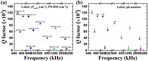
Table 1. The pit numbers of various SCD cantilevers with different Q factors.
4. Conclusions
In a summary, we examined the effects of SCD crystal quality and the etch pits on the Q factors of the SCD cantilevers. Due to the introduction of ion-damaged layer in the substrate layer, the Q factors of the SCD cantilevers were limited. The etching in an oxygen ambient provided an effective approach to remove the ion-damaged layer and the surface dislocation defects and, in turn, improve the Q factors of the SCD resonators from thousands up to 120 000. Through the 2D Raman imaging technique, the precise dislocation positions and the dislocation-induced local stress of the SCD epilayer were visualized. The relationship between the FWHM of the Raman spectra and the Q factors was realized, showing that a low FWHM of the SCD resonator contributed to a high Q factor. Although the dislocations were etched to form the etch pits, it was noted that there was no obvious dependence of the Q factors on the numbers of the etch pits on the SCD resonators.
Author contributions
Zilong Zhang: conceptualization, methodology, investigation, writing-original draft and editing, writing-review and editing. Guo Chen: writing-editing. Keyun Gu: writing-editing. Satoshi Koizumi: writing-editing. Meiyong Liao: supervision, conceptualization, writing-original draft review and editing, writing-review and editing.
Supporting information
Supporting information is available from the author.
Supplemental Material
Download MS Word (1.1 MB)Disclosure statement
No potential conflict of interest was reported by the authors.
Additional information
Funding
References
- Liao M, Koide Y, Sang L. Single crystal diamond micromechanical and nanomechanical resonators. Novel aspects of diamond. Berlin: Academic Press; 2019.
- Liao M. Progress in semiconductor diamond photodetectors and MEMS sensors. Funct Diam. 2021;1(1):1–9.
- Zhang Z, Wu H, Sang L, et al. Single-crystal diamond microelectromechanical resonator integrated with a magneto-strictive galfenol film for magnetic sensing. Carbon. 2019;152:788–795.
- Tao Y, Boss JM, Moores B, et al. Single-crystal diamond nanomechanical resonators with quality factors exceeding one million. Nature Commun. 2014;5(1):3638.
- Olivero P, Rubanov S, Reichart P, et al. Ion-beam-assisted lift-off technique for three-dimensional micromachining of freestanding single-crystal diamond. Adv. Mater. 2005;17(20):2427–2430.
- Vashist SK. A review of microcantilevers for sensing applications. J Nanotech. 2007;3:1–18.
- Imboden M, Mohanty P. Dissipation in nanoelectromechanical systems. Phys Rep. 2014;534(3):89–146.
- Cleland AN. Thermomechanical noise limits on parametric sensing with nanomechanical resonators. New J. Phys. 2005;7(1):235–235.
- Yasumura KY, Stowe TD, Chow EM, et al. Quality factors in micron-and submicron-thick cantilevers. J. Microelectromech. Syst. 2000;9(1):117–125.
- Zhang Z, Wu Y, Sang L, et al. Coupling of magneto-strictive FeGa film with single-crystal diamond MEMS resonator for high-reliability magnetic sensing at high temperatures. Mater Res Lett. 2020;8(5):180–186.
- Zhang Z, Wu H, Sang L, et al. Enhancing Delta E effect at high temperatures of galfenol/Ti/single-crystal diamond resonators for magnetic sensing. ACS Appl. Mater. Interfaces. 2020;12(20):23155–23164.
- Liao M, Toda M, Sang L, et al. Energy dissipation in micron-and submicron-thick single crystal diamond mechanical resonators. Appl. Phys. Lett. 2014;105(25):251904.
- Wu H, Sang L, Li Y, et al. Reducing intrinsic energy dissipation in diamond-on-diamond mechanical resonators toward one million quality factor. Phys Rev Mater. 2018;2(9):090601.
- Tallaire A, Ouisse T, Lantreibecq A, et al. Identification of dislocations in synthetic chemically vapor deposited diamond single crystals. Cryst Growth Des. 2016;16(5):2741–2746.
- Achard J, Tallaire A, Mille V, et al. Improvement of dislocation density in thick CVD single crystal diamond films by coupling H2/O2 plasma etching and chemo-mechanical or ICP treatment of HPHT substrates. Phys. Status Solidi A. 2014;211(10):2264–2267.
- Friel I, Clewes S, Dhillon H, et al. Control of surface and bulk crystalline quality in single crystal diamond grown by chemical vapour deposition. Diam Relat Mater. 2009;18(5–8):808–815.
- Ovartchaiyapong P, Pascal L, Myers B, et al. High quality factor single-crystal diamond mechanical resonators. Appl. Phys. Lett. 2012;101(16):163505.
- Liao M, Toda M, Sang L, et al. Improvement of the quality factor of single crystal diamond mechanical resonators. Jpn. J. Appl. Phys. 2017;56(2):024101.
- Liao M, Li C, Hishita S, et al. Batch production of single-crystal diamond bridges and cantilevers for microelectromechanical systems. J. Micromech. Microeng. 2010;20(8):085002.
- Sun H, Sang L, Wu H, et al. Effect of deep-defects excitation on mechanical energy dissipation of single-crystal diamond. Phys. Rev. Lett. 2020;125(20):206802.
- Xu J, Lu K, Fan D, et al. Different etching mechanisms of diamond by oxygen and hydrogen plasma: a reactive molecular dynamics study. J. Phys. Chem. C. 2021;125(30):16711–16718.
- Tsubouchi N, Mokuno Y, Shikata S. Characterizations of etch pits formed on single crystal diamond surface using oxygen/hydrogen plasma surface treatment. Diam Relat Mater. 2016;63:43–46.
- Weaver TW, Young SP, et al. Vibration problems in engineering. Hoboken, USA: Academic Press; 1974.
- Ivanov O, Muchnikov A, Chernov V, et al. Experimental study of hydrogen plasma etching of (100) single crystal diamond in a MPACVD reactor. Mater Lett. 2015;151:115–118.
- Yurov V, Bushuev E, Bolshakov A, et al. Etching kinetics of (100) single crystal diamond surfaces in a hydrogen microwave plasma, studied with in situ low-coherence interferometry. Phys. Status Solidi A. 2017;214(11):1700177.
- Seitner MJ, Gajo K, Weig EM. Damping of metallized bilayer nanomechanical resonators at room temperature. Appl. Phys. Lett. 2014;105(21):213101.
- Khokhryakov AF, Palyanov YN. Revealing of dislocations in diamond crystals by the selective etching method. J Cryst Growth. 2006;293(2):469–474.
- Shimaoka T, Ichikawa K, Koizumi S, et al. Detection of defects in diamond by etch‐pit formation. Phys. Status Solidi A. 2019;216(21):1900247.
- Gaukroger M, Martineau P, Crowder M, et al. X-ray topography studies of dislocations in single crystal CVD diamond. Diam Relat Mater. 2008;17(3):262–269.
- Teraji T, Yoshizaki S, Mitani S, et al. Transport properties of electron-beam and photo excited carriers in high-quality single-crystalline chemical-vapor-deposition diamond films. J Appl Phys. 2004;96(12):7300–7305.
- Hoa LTM, Ouisse T, Chaussende D, et al. Birefringence microscopy of unit dislocations in diamond. Cryst Growth Des. 2014;14(11):5761–5766.
- Ichikawa K, Shimaoka T, Kato Y, et al. Dislocations in chemical vapor deposition diamond layer detected by confocal raman imaging. J Appl Phys. 2020;128(15):155302.
- Von Kaenel Y, Stiegler J, Michler J, et al. Stress distribution in heteroepitaxial chemical vapor deposited diamond films. J Appl Phys. 1997;81(4):1726–1736.
- Shen X, Lv Z, Ichikawa K, et al. Stress effect on the resonance properties of single-crystal diamond cantilever resonators for microscopy applications. Ultramicroscopy. 2022;234:113464.