
 ?Mathematical formulae have been encoded as MathML and are displayed in this HTML version using MathJax in order to improve their display. Uncheck the box to turn MathJax off. This feature requires Javascript. Click on a formula to zoom.
Abstract
The nitrogen vacancy (NV) color centers are a solid-state quantum system with the ability to maintain long coherence times at room temperatures. NV centers have potential applications in quantum detection, which necessitates their positioning at minimal distances from surfaces. However, the existing methods for fabricating NV centers are cumbersome, expensive, and difficult to control. This study investigates the etching mechanism of transition metals on diamond under plasma conditions and develops a method for producing shallow NV centers on the surface of high pressure and high temperature diamond. Our proposed method enables the production of shallow NV centers below the surface in the longitudinal direction, while simultaneously allowing precise control over the lateral distribution. Moreover, the operating costs associated with our technique are significantly lower than those of ion implantation and electron irradiation. This research contributes to the advancement of iron-etching diamond processing technology, and the proposed method facilitates the more portable preparation of shallow color centers in specific regions, enabling the realization of locally controllable and scalable coupled quantum systems.
1. Introduction
In contrast to superconducting quantum bits [Citation1, Citation2], cold atoms [Citation3, Citation4], and ion-trap systems [Citation5, Citation6] (which require extreme low-temperature or ultra-high-vacuum experimental conditions), nitrogen vacancy (NV) color centers in diamond form a solid-state quantum system that can be manipulated and read out at room temperature [Citation7–9]; this has a considerable potential for applications in quantum detection [Citation10–13]. As a magnetic-field-sensitive unit [Citation14–16], the closer the NV color center is to the measurement object, the stronger the measured signal [Citation17, Citation18]. Therefore, in practical applications, the NV color center is often required to be as shallow as possible below the diamond surface [Citation19, Citation20]. There are four traditional methods for preparing color centers: direct growth [Citation21, Citation22], electron irradiation [Citation23, Citation24], ion implantation [Citation25, Citation26], and femtosecond laser writing [Citation27, Citation28]. The direct growth method can control the distribution of color centers in the longitudinal direction, whilst the other three methods can precisely control their position in the lateral one. Complex procedures and expensive equipment are often required to produce color centers in a controlled manner.
This article describes a method for inducing a highly efficient etching reaction on the surface of HPHT diamond samples by depositing transition metal iron and subjecting them to a plasma environment. By employing this method, we successfully prepared shallow NV color centers on the surface of the samples. Furthermore, we were able to control the spatial distribution of the NV color centers by utilizing photolithography techniques to control the distribution of the metal pattern. In addition to preparing NV color centers on the surface of HPHT diamond, this method can also be utilized to enhance the conversion efficiency of vacancy-related color centers in CVD diamond. We conducted an analysis of the NV color center formation process and discussed the mechanism of etching diamond surfaces by transition metal iron and nickel. Additionally, we provided empirical parameters for vacancy migration kinetics in diamond. The research conducted in this study on the etching mechanism of diamond surfaces by transition metals is expected to contribute to the advancement of this highly efficient and cost-effective processing technology. And the presented new preparation method of NV color centers significantly reduces the cost of precisely positioning color centers, thereby promoting the development of various quantum detection applications based on shallow color centers. Moreover, the method is expected to have applications in locally controllable and scalable coupled quantum systems.
2. Method
The samples consisted of six pieces of single crystal HPHT diamond (within rich substitutional nitrogen atoms) and one piece of single crystal chemical vapor deposition (CVD) diamond (within rich NV centers and SiV centers), all of which featured (100) crystalline structures and were polished to 30 nm roughness; the remaining samples (used for reproducibility verification) are not described here. Cleaning and metal-pattern preparation procedures were identical for all samples. The samples were cleaned via ultrasonication in acetone, deionized water, and alcohol for 30 min [Citation29]. A standard UV lithography lift-off process was performed to define the metal pattern, using a MicroWriter ML3. A 50-nm Fe film was deposited on the diamond surface via magnetron sputtering. Subsequently, the diamond samples, which had been deposited with iron, were placed onto a sample holder with water cooling within the microwave plasma CVD system. This CVD system provides the required plasma environment for etching the diamond with iron. The reaction gas used within the chamber is hydrogen, with a flow rate of 300 sccm and a pressure of 72 Torr, while the power is set to 2300 W to achieve a diamond surface temperature of 800 °C. It is noteworthy that the key parameters for the reaction are the type of gas and the reaction temperature, and the adjustment of pressure and power is necessary to ensure that the sample surface reaches the target temperature. Following a one-hour hold at these conditions, the pressure and power are increased to 85 Torr and 2500 W, respectively, to raise the sample surface temperature to 980 °C, which is then maintained for another hour. Subsequently, the pressure and microwave power are gradually decreased to cool the sample surface down to room temperature. After etching, the samples were placed in a mixed solution of concentrated sulfuric acid and concentrated nitric acid at 230 °C for 30 min; then, the solution was heated to 350 °C for 1 h. The purpose of this step was to remove the residual metal particles and surface graphite.
To investigate the mechanism, six control groups were set, and the diamond type, reaction temperature, etching surface direction, deposited metal type, hydrogen atmosphere, and vacuum were set as variable conditions (). The two final samples were reacted in a tubular furnace. All samples were measured using a Horiba HR Evolution Raman spectrometer. The excitation light power was 10 mW, the grating was 1800 g/mm, the confocal aperture was 50 μm, the objective lens magnification was 50×, and the numerical aperture was 0.5. The surface topography was characterized using laser confocal microscopy and scanning electron microscopy (SEM). The metal did not exhibit a Raman signal; hence, X-ray photoelectron spectroscopy (XPS) and energy dispersive spectroscopy (EDS) were used to characterize the presence of residual metal in the cleaned sample. The response of the NV centers to magnetic field and related spin coherence properties were characterized using an optically detected magnetic resonance (ODMR) system.
Table 1. Processing parameters of different samples.
3. Results
The photolithography pattern was entirely controllable. However, the limitations of the lithography machine model meant that the smallest possible pattern size in this experiment was ∼1 μm. In the reported literature studies, metal etching of the diamond only shows a certain degree of anisotropy in terms of the crystal orientation angle [Citation30]; furthermore, the influence of the shape of the metal itself upon the etching effect is often neglected. In this study, square, diamond, triangular, and circular patterns were deposited on the remaining HPHT samples (), and a Chinese character was deposited on Sample S-C1 (Figure S1a). After two hours of high-temperature plasma treatment, the iron-deposited areas formed etch pits on the diamond surface; these correspond to the dark regions in and Figure S1b, as obtained using a laser confocal microscope. The color distribution in represents the relative height of each region, which is caused by the unevenness of the sample stage; while the dark regions significantly represent the distribution of etch pits. And the depth of the etch pit reached the order of microns. The etched area exhibits an etch pattern consistent with the deposited metal one; however, the straight lines in Figure S1a are curved (as shown in Figure S1b). We believe that this is because the combination of a small metal film thickness (only 50 nm) and relatively small pressure reduces the melting point [Citation31]. In actual operations, the surface metal can be observed to roughen when the temperature increases to 400 °C; this indicates that the melting point has been reached. Therefore, at the etching temperature, a slight Leidenfrost phenomenon occurs at the interface between the metal and diamond [Citation32], causing it to shift from its original position and producing pattern distortion. However, the pattern on the surface of the HPHT sample is symmetrical (); thus, the force is uniform around the pattern, which reduces the possibility of pattern distortion.
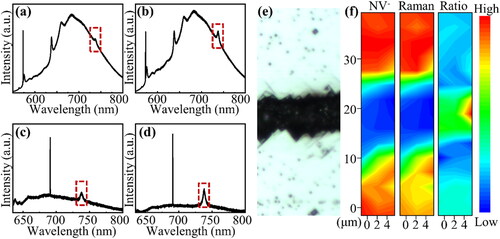
Figure 1. (a, b) Comparison of before and after iron etching. (a) Regular photolithography pattern on HPHT samples. (b) Etching pattern on Sample S-Ha. (c, d) Raman spectra for etched and unetched regions of Sample S-Ha after high-temperature plasma treatment. (c) Unetched region, containing only the first-order Raman characteristic peak of diamond in the spectrum. (d) Etched region, where the peaks at 1405.7 cm−1 (575 nm) and 3098.4 cm−1 (637 nm) correspond to the neutral and negative charge states of the NV center, respectively. These two peaks confirm the presence of NV centers.
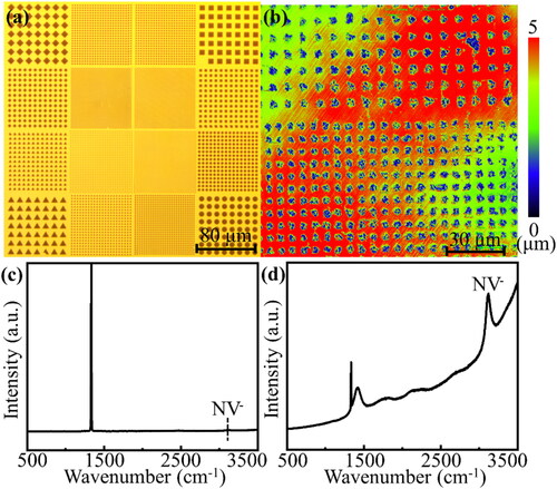
shows the Raman spectrum of the undeposited metal area (i.e. unetched area) for Sample S-Ha, which was treated with high-temperature plasma and preserved. The Raman spectrum of this sample before plasma treatment is similar to and is shown in Figure S2. shows that Sample S-Ha itself does not contain any NV color centers, and it precludes the possibility that the etching effect of hydrogen plasma on diamond can produce NV color centers. depicts the Raman spectrum of the iron-etched area. There are two notable peaks in the spectrum, at 1405.7 cm−1 (575 nm) and 3098.4 cm−1 (637 nm); these correspond to the two zero-phonon lines (ZPLs) of NV centers [Citation33]. It is shown here that the HPHT diamond, which originally features no color center, produces NV color centers on its surface after iron etching.
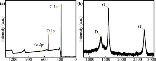
To eliminate the influence of the iron-carbon solid solutions or surface plasmons (generated by nano-iron particles) on the photoluminescence measurement, XPS measurements () were used to prove that iron elements within a few hundred microns of the surface were completely cleaned. The EDS results for the etched area indicate that the number of Fe atoms accounted for only 0.01% of the material near the sample surface. Considering the machine error, it can be concluded that no Fe atoms were present in the etched microscopic area. Graphite is another impurity that can be present on the surface. According to previous reports, carbon atoms in diamond are dissolved in iron during the etching process, and they react with hydrogen to form methane after precipitation on the upper surface [Citation34–36]. Furthermore, at ∼800 °C, graphite can react with hydrogen via a catalytic transition to generate methane [Citation37, Citation38]. This suggests that the carbon on the metal surface precipitates in the form of graphite. However, no graphite peak was observed in . This is reasonable because hydrogen plasma has a stronger etching effect on graphite than on diamond [Citation39, Citation40]. To prove the above argument, Sample S-Hc was turned over during plasma treatment, which was conducted under the same reaction conditions as Sample S-Ha. In other words, the metal-plated side remains in contact with the sample holder, whereas the non-metal-plated side remains in contact with the plasma. Although the metal-plated side is in contact with the holder, a gap must be present between the two sides, owing to the lack of bonding agent. Therefore, it can be considered that the metal-plated side is not in contact with the plasma but rather a thin hydrogen atmosphere. The thermometer can only measure the diamond temperature on the upper surface, and the lower surface is close to the water-cooled substrate; thus, the actual temperature of the lower surface is lower than 980 °C. However, because of the high thermal conductivity of diamond [Citation41] and the overall redness during etching (diamond emits notably red-wavelength radiation at temperatures exceeding 800 °C), we estimate that the temperature of the lower surface should only fall slightly to 850 °C. Raman spectroscopy was performed on the iron-plated area of Sample S-Hc (). The three peaks in correspond to the D, G, and G’ peaks of graphite [Citation42, Citation43], and no signal for the characteristic diamond Raman peak was observed. This confirms that the carbon atoms in the contacted part of diamond and iron are precipitated on the iron surface in the form of graphite after dissolution in iron; they subsequently accumulate on the surface, entirely concealing the diamond signal. After the graphite was removed via acid boiling, the Raman spectrum of Sample S-Hc was obtained, as shown in Figure S3; furthermore, no NV color center signal was observed when compared with Sample S-Ha.
Figure 2. (a) XPS results for etched diamond surface after cleaning. No signal for residual iron was observed. (b) Raman spectrum of iron-plated area in Sample S-Hc after high-temperature plasma treatment. The three peaks in the spectrum correspond to graphite, which indicates that carbon atoms precipitate graphite on the diamond surface and mask the diamond Raman signal.
The lack of NV color centers in Sample S-Hc can be attributed to the decrease in temperature compared to Sample S-Ha and the lack of exposure to the plasma. Hence, four additional sets of comparative experiments were performed. The differences (compared to Sample S-Ha) consisted of a decrease in the experimental temperature (to 850 °C) for Sample S-Hb, the use of nickel as the deposited metal for Sample S-Hd, a hydrogen atmosphere heating environment for Sample S-He, and a vacuum heating environment for Sample S-Hf. The etching effect was observed in all samples; however, the NV color centers were only present in Samples S-Ha and S-Hd, and the spectra for the etched areas of the remaining samples were consistent with the HPHT diamond. This indicates that the generation of NV centers via etching is related to the temperature and heating environment; the exact relationship will be discussed in detail later.
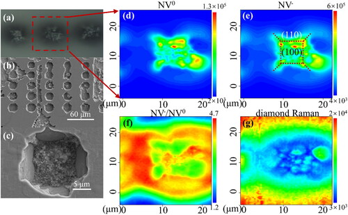
The distribution of color centers in the etched area helps to illustrate the relationship between metal etching and NV color center generation. The SEM micrographs and photoluminescence (PL) mapping of the etched area for Sample S-Ha are shown in . shows a focusing micrograph of the PL measurements. The focal plane was focused on the etched pit, and the unetched area around it was unfocused because of the height difference between the etch pit and diamond surface. shows the SEM image of a larger area. The entire surface is clean and free from residual particulate impurities. shows an SEM image of one of the etched pits in . The walls surrounding the pits are smooth (110) crystal surfaces [Citation44]. The square shape of the pit bottom indicates that the etching was anisotropic. The pit bottom appears rough because it shows numerous small square pits at high magnification (similar to fractals). shows PL contour maps in the mapping mode; these correspond to the spectral integrated area of ZPL and phonon sidebands (574–590 nm) for NV0 color centers, the spectral integrated area of ZPL and phonon sidebands (630–650 nm) for NV- color centers, the spectral integrated area ratio of NV- to NV0 color centers, and the intensity of the first-order diamond Raman peak, respectively. show a color center signal in the etched area, whereas none is observed in the unetched one. This shows once again that the etching effect of diamond by iron leads to the generation of NV color centers. The distributions of the NV0 and NV- color centers are in perfect agreement, which indicates the reliability of the spectral scanning process. The distribution of the ratio between NV- and NV0 is mostly uniform, with a slight increase in the center when considering only the area containing NV color centers. It is generally understood that one extra electron in NV- originates from nitrogen donor impurities [Citation45], and a larger ratio in the central region may expose the electron interactions between different crystal orientations at the edges of the etched region. In the unetched area, the larger ratio may be attributable to the fact that the integral spectral range of NV- is slightly larger than that of NV0. The dashed box in shows the crystal planes and color center distribution. The NV color centers filled the (100) plane and were distributed at the intersection of each crystal plane. shows that the boundary is not clear and features rough bumps between adjacent (110) interfaces, which may explain the presence of color centers at the intersection. The intensity of the first-order diamond Raman peak in reflects the orderliness of the diamond lattice. Because the focal plane is in the etched pit, the intensity of the first-order Raman peak in the non-etched region should be twice as high as that in the etched region, considering the distribution of the laser spot along the z-axis. However, in , the intensity in the etched region is only 0.25 times that in the non-etched region, which means that the lattice order in the etched region is smaller than that in the non-etched one. Nitrogen atoms are abundant in HPHT diamonds, and the NV color centers are composed of nitrogen atoms and vacancies. Therefore, the NV color center generation in the etched region must be due to the formation of vacancies in the lattice. Vacancies, as a type of point defect, lead to poor lattice ordering. Therefore, when the Raman intensity is weak, the corresponding color-centered signal intensity is large. The color-center generation mechanism is here presented. The etching of diamond by iron destroys the orderliness of the diamond lattice, thereby introducing vacancies thereinto; these vacancies migrate further and are captured by substitutional nitrogen atoms to form color centers. However, it is worth noting that this explanation can only be applied for samples that have produced color centers, and further discussion is still required for samples that undergo iron etching but do not produce color centers.
Figure 3. (a) Focusing micrograph when conducting PL mapping measurements; the defocusing is attributable to the height difference between the etching pit and surface. (b) SEM image of the etched diamond surface. (c) SEM image of one of the etched pits in (b). (d–g) PL contour maps for the etched pit. (d) Spectral integrated area of ZPL and phonon sidebands (574–590 nm) for NV0 color centers. (e) Spectral integrated area of ZPL and phonon sidebands (630–650 nm) for NV- color centers. (f) Spectral integrated area ratio of NV- to NV0 color centers. (g) Intensity of first-order diamond Raman peak.
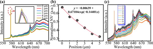
To probe the position of the color center below the surface, we sought to determine it by varying the focus position in the longitudinal direction and the hole parameters in the confocal system. As shown in , the focusing plane was moved from the surface in steps of 1–5 μm. As the measurement depth increased, the signal intensity of the first-order Raman peak increased slightly, owing to the increase in acquisition area. However, it should be noted that the increase was not very large (inset in ) because the entire optical system was confocal and could maximally shield the signal near the unfocused surface. In contrast, the signal intensities of the NV0 ZPL at 575 nm and NV- ZPL at 637 nm gradually weakened under the increasing test depth. This indicates that most NV color centers are concentrated in the surface region. The intensities of the NV color centers at different depths were normalized by the intensity of the first-order Raman peak signal, to produce a fitted curve (). The fitting function was deduced from Fick’s first law, based on the diffusion of vacancies (Eq. S5 in Supplementary Material):
(1)
(1)
Figure 4. (a) PL spectra for different focusing planes from the surface in steps of 1–5 μm. The intensity of NV0 and NV- centers decreases significantly with the increase of focusing depth, whilst the intensity of the first order diamond Raman peak increases slightly (inset). (b) Fitted curve for depth and intensity of NV color centers, normalized by the intensity of the first-order Raman peak signal. This curve satisfies Fick’s first law. (c) PL spectra for different hole apertures (the unit in the legend is μm) whilst focusing the diamond surface. When the hole aperture is 10 μm, the relative NV centers signal intensity is largest, which indicates that the NV centers are distributed in the range of 50 nm below the surface.
This curve describes the change of NV centers signal intensity with depth, so under the premise that the PL intensity is proportional to the number of NV centers, it can also describe the distribution of NV centers in depth. And the generation of NV centers comes from the introduction of vacancies, so this curve can also describe the migration kinetics of vacancies within the diamond crystal.
Clearly, a spatial resolution of micron size cannot accurately describe the distribution of color centers. Thus, we attempted to use a pinhole in the confocal system to further refine the distribution of color centers in the longitudinal direction. The significance of the hole is that the smaller its value, the smaller the z-axis range acquired by the microscope and the closer it is to an ideal plane. After focusing the focal point on the diamond surface, the fluorescence intensity was measured whilst decreasing the hole aperture. As the hole aperture decreased, the longitudinal range of the collected signal decreased, the signal intensity decreased, and the curve changed from rough to smooth. The ratio of the NV color center fluorescence intensity to the diamond Raman peak intensity in the spectrum can qualitatively determine the number of NVs per unit volume in the detection range. The fluorescence intensity for each hole parameter was normalized by the intensity of the first-order Raman peak signal, as shown in . We observed that the relative fluorescence intensity of the color center was largest at a hole aperture of 10 μm, which indicates that the NV color center is the most concentrated in this range. In the Supplementary Material, it is demonstrated (from the optical path) that the collection range is within the 50 nm range for the hole with an aperture of 10 μm. Therefore, it can be assumed that the main distribution range of the color centers is within 50 nm of the surface; thus, they can be referred to as shallow color centers.
According to the previous discussion, the creation of vacancies leads to the creation of NV color centers. For further proof, we used a piece of CVD diamond (S-C1) containing NV and SiV color centers for experimental verification. show the spectra before and after etching, respectively. It can be found that the intensity of the NV- center changes from below the first-order Raman peak before etching to above it afterward, and the fluorescence intensity of the SiV color center (red box) at 738 nm is also significantly enhanced. The fluorescence intensity at 738 nm represents the superposition of the intensity of the phonon sideband of the NV- center and the ZPL of the SiV- center, and 70% of the fluorescence intensity of the SiV color center is concentrated on the ZPL [Citation46]. Thus, the fluorescence intensity of the SiV- center can be roughly estimated as having been enhanced by a factor of 2–3 after removal of the phonon sidebands from the NV- center. To filter out the effect of the NV color center, measurements were performed using a 633 nm laser, and the spike at 691.3 nm in corresponds to the Raman shift of diamond at 1332 cm−1. The enhancement of the SiV- centers’ fluorescence after etching can be seen more clearly without interference from the NV centers’ fluorescence. This implies an increase in the number of SiV color centers, attributable to the introduction of vacancies; this further illustrates the effect of iron etching on diamonds. show micrographs of the etched and nearby unetched regions and the fluorescence contour map, respectively. Because the focusing surface lies on the surface of the unetched region, the signal intensity of the etched region is low. However, we found that the relative intensity of NV- centers in the etched region exceeds that in the unetched region, by normalizing the intensity of NV- centers as the first-order Raman peak of diamond. Two suggestions are proposed regarding the enhancement of the color center fluorescence. First, the rough structure in the etched pit can effectively mitigate the total reflection effect of the plane when the fluorescence of the color center is scattered outward. Second, the vacancy introduced by the etching enhances the conversion rate of impurity atoms to color centers. It is also possible that the combination of these two effects enhances the color center fluorescence. Thus, the iron etching optimizes the fluorescence of color centers in diamond.
Figure 5. (a) PL spectrum of unetched region under 532 nm laser excitation. (b) PL spectrum of etched region under 532 nm laser excitation. (c) PL spectrum of unetched region under 633 nm laser excitation. (d) PL spectrum of etched region under 633 nm laser excitation. The intensity of SiV- centers strengthens after etching. (e) Micrographs of the etched region and nearby unetched region. (f) The contour map of NV- center intensity, diamond Raman peak intensity, and the ratio therebetween. The relative intensity of NV- centers in the etched region exceeds that in the unetched one.
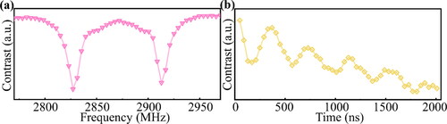
The quality of the NV centers in Sample S-Ha was measured using an ODMR system. shows the ODMR spectrum of Sample S-Ha under an external magnetic field. The splitting of the two peaks indicates the response of the NV ensemble prepared by iron etching to the magnetic field, as well as the Rabbi oscillation occurring under this magnetic field (). The spin state depopulation time T1 and the spin coherence time T2 was measured in Figure S5. All fitting formulas are in the Supplementary Material.
Figure 6. Characteristics of NV center spin parameters, as obtained by ODMR system, for (a) ODMR spectrum, and (b) Rabi oscillation measurement.
4. Discussion
One of the clearest parameters for metal-etched diamond is the etching depth, which can indicate the etching efficiency. lists the etching depths of the samples discussed in this study, among which no CVD samples were included. This is because the defect density of the CVD sample was markedly higher than that of the HPHT sample, which resulted in errors. shows the relationship between the etching effect of metals on diamonds and the presence of NV color center signals. Several conclusions can be drawn from the table: (1) Without hydrogen participation, the etching rate is very low; (2) the etching rate of hydrogen plasma exceeds that of the hydrogen atmosphere; (3) a temperature window is present in the iron-etched diamond, and a higher temperature does not imply a faster etching rate; (4) the etching efficiencies of different metals on diamond are inconsistent, and the effect of Ni is significantly worse than that of Fe, consistent with Ref. [Citation47].
Table 2. Etching depths under different processes.
It is worth noting that the purpose of using 800 °C for one hour before 980 °C is to minimize the influence of the Leidenfrost phenomenon and ensure the integrity of the metal pattern. By first processing at a lower temperature, a more ideal etching pattern can be obtained in the early stage, and the sinking metal will be fixed. Then, by raising the temperature, the shape of the pattern will not be destroyed.
We propose the following model to explain the mechanism of iron etching and the production of NV color centers. When the temperature exceeds 800 °C (the migration threshold temperature of vacancies [Citation48]), the carbon at the interface between iron and diamond dissolves in the iron and forms an iron-carbon solid solution (). Then, the carbon dissolved in the lower surface diffuses to the upper surface (), driven by the concentration gradient; finally, it precipitates on the surface of the iron (). The precipitated carbon is present in the form of graphite (), which reacts with the hydrogen plasma or hydrogen atmosphere to form CxHyz+ or methane volatilization from the surface. The volatile carbon on the surface forms a concentration gap, forcing the carbon on the lower surface to continue to dissolve in the iron and migrate upward. Finally, the entire piece of iron sinks down on the diamond surface and forms an etching pit. It should be noted that the reaction between the hydrogen plasma and graphite is much faster than that with the hydrogen atmosphere, which means a larger concentration gradient driving force is present in the hydrogen plasma than in the hydrogen atmosphere. A larger concentration gradient driving force can ensure a faster rate of carbon dissolution at the interface (), with the possibility of disrupting the crystal structure and thereby creating vacancies (). The vacancies are thermodynamically driven to diffusion, and the diffusion rate is temperature dependent [Citation49],
(2)
(2)
where D is the diffusion coefficient, Ea is the activation energy for vacancy diffusion, k is the Boltzmann constant, T is the temperature, and D0 is a pre-factor.
Figure 7. The process of producing NV centers in diamond via iron etching: (a) iron film is deposited on the diamond surface. (b) The carbon atoms at the interface between the iron and diamond dissolve in iron. (c) The carbon atoms dissolved in the lower surface diffuse to the upper surface, driven by the concentration gradient. (d) The diffused carbon atoms precipitate in the form of graphite on the iron surface. (e) The violent reaction between hydrogen plasma and graphite accelerates the dissolution of carbon atoms at the interface into iron, generating vacancies. (f) The generated vacancies migrate and are captured by the substituted nitrogen atoms to form NV centers.
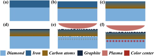
The diffused vacancies are trapped and combined by the substituted nitrogen atoms within the diamond to form a more stable NV structure [i.e. the NV color center ()]. In a hydrogen atmosphere, the reaction of hydrogen with graphite is apparently much more retarded; this is strongly supported by the small graphite signal still found in the Raman spectrum of the S-He sample (Figure S6). The slow oxidation reaction of graphite and hydrogen, which occurs at the iron surface, leads to a gentle dissolution of carbon at the interface; this helps to preserve the integrity of the lattice but cannot produce vacancy defects and therefore cannot form color centers.
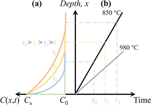
For Sample S-Hb, the etching rate was three times higher than that of sample S-Ha, though no signal from the NV center was detected. As mentioned previously, a temperature window exists for the iron etching rate, and the reaction temperature of S-Hb should lie exactly within this temperature window; this leads to a faster etching rate (). The lower temperature reaction conditions of Sample S-Hb result in a lower vacancy migration rate than that of Sample S-Ha (EquationEquation (2)(2)
(2) ). Therefore, it is possible that the vacancy migration rate of the S-Hb sample is lower than the iron etching rate, which means that the vacancies are etched away before diffusion (). The high-temperature conditions of Sample S-Ha slightly above the temperature window suppress the etching efficiency and increase the vacancy diffusion rate, which provides the opportunity for the vacancies to diffuse downward and thereby form NV centers. It should be noted that Sample S-Ha was pre-treated at 800 °C to avoid the Leidenfrost effect, which leads to the distortion of the etching pattern. To summarize, the necessary conditions for NV center generation on diamond surfaces using iron etching are as follows: (1) the external hydrogen plasma produces a large driving force that makes it possible to generate vacancies in the dissolution of carbon in iron, and (2) the reaction temperature is in a suitable range (e.g. 950 °C) to ensure that the vacancy migration rate exceeds the iron etching rate, to protect the formed NV centers.
Figure 8. (a) Distribution of vacancies with respect to depth at different times for a given initial concentration Cs at an initial location. The curve is derived by Fick’s second law (Eq. S12). (b) Etching depth dependence on time at different temperatures. At 850 °C, the distribution depth of vacancies is always smaller than the etching depth; thus, no NV centers can be formed.
For Sample S-Hd, the etching depth was small, although the experimental conditions were identical to those for Sample S-Ha. This is because, although Ni can also catalytically etch diamond [Citation34], it is difficult to form an effective solid solution with carbon. After etching, the iron-etched samples were observed to form iron-carbon compounds, whilst the nickel-etched samples were still essentially in pure nickel form [Citation50]. However, it is noteworthy that a similar signal for NV centers was observed for the S-Hd sample. This suggests that nickel and iron produce similar catalytic etching effects upon the diamond surface during the early stages of etching, and they dissolve carbon atoms to create vacancies. The difference is that, in the presence of nickel, the carbon atoms migrate along the outer side of the nickel [Citation51] and are eventually distributed on the surface, to react with the hydrogen plasma there. Thus, after certain etch depth is formed, the sunken nickel is embedded and prevents the etching reaction from proceeding further, resulting in a shallow etch depth. Sample S-Hd reaffirms the mechanism of NV center generation discussed in the previous paragraph; that is, strong etching produces vacancies, and when the etching rate is below the migration rate of vacancies, NV centers are formed in the surface layer. In addition, this study presents a new perspective on the experimental etching of diamonds by metal, in which defects are introduced in the surface layer during etching; this has not been mentioned in previous studies.
5. Conclusion
In the present study, we successfully produced position-controlled NV color centers on a diamond surface, by employing the etching effects of transition metals (Fe and Ni) on diamond. The prerequisites for obtaining NV color centers were the correct choice of metal and hydrogen plasma, as well as an appropriate temperature interval. The generation of color centers is attributed to the fact that the dissolution of carbon from diamond to transition metal intensifies in the hydrogen plasma, resulting in vacancies at the interface. When the migration rate of vacancies exceeds the dissolution rate of carbon atoms, the diffused vacancies are likely to be captured by the substituted nitrogen atoms and form NV color centers. On a sample containing SiV color centers (Sample S-C1), we further demonstrated that vacancies were created during the Fe etching process, and SiV- fluorescence was effectively enhanced. We also tested the spin properties of the generated NV color centers, which could undergo effective Zeeman splitting under an external magnetic field. Nevertheless, the coherence properties of the samples were poor, and further optimization will be needed in follow-up studies, such as adding oxygen plasma to enhance the wettability between metal and diamond, high temperature annealing to improve crystallinity, and surface terminal treatment.
Compared with the reported methods of electron irradiation, direct growth, ion implantation, and femtosecond laser writing, we propose a new method which can produce shallow NV ensemble and precisely control the distribution in the lateral direction. The minimum feature size we have managed to achieve in this study is approximately 1 μm. However, it’s important to note that the lateral precision in this study is primarily contingent upon the intricacies of the mask preparation process. Consequently, the lateral precision of metal etching can attain a level comparable to that of ion implantation or electron irradiation, achieving dimensions in the order of tens of nanometers, and surpassing the capabilities of laser writing at around 1 μm (adhering to the optical diffraction limit) and the CVD technique. With regards to depth positioning accuracy, the vacancies generated by metal etching originate from the interface between diamond and metal, resulting in the primary distribution of prepared NV centers near the surface. Consequently, when producing shallow NV color centers, metal etching methods may indeed possess certain advantages. However, concerning deep positioning precision, it falls short in comparison to the accuracy achievable through ion implantation and laser direct writing.
In addition, we observed the diffusion process of vacancies in diamond through the characterization of NV color centers. And we accurately describe the process of iron etching diamond and reconfirm the mechanism of nickel etching on diamond from an additional perspective consistent with Ref. [Citation51]. This suggests a new research approach for monitoring changes in the diamond crystal state by means of color centers.
To conclude, our research demonstrates a novel method for the preparation of shallow color centers with a controlled positional distribution; this will help enhance regionally controllable and scalable quantum systems, and it makes a significant contribution to the fields of quantum computing and quantum detection.
Author contributions
The manuscript was written through contributions of all authors. Sen Zhang: Conceptualization, Data curation, Formal analysis, Investigation, Methodology, Resources, Validation, Visualization, Writing – original draft. Jiwen Zhao: Investigation, Validation, Methodology. Yicun Li: Investigation, Validation, Methodology. Xiaobin Hao: Investigation, Methodology. Xiaohui Zhang: Investigation, Methodology. Pengfei Qiao: Investigation, Validation, Methodology. Ying Liang: Investigation, Validation, Methodology. Bo Liang: Investigation. Wenchao Zhang: Validation. Wenxin Cao: Validation. Lei Yang: Investigation. Bing Dai: Conceptualization, Visualization. Kang Liu: Funding acquisition, Methodology, Project administration, Supervision, Writing – original draft, Writing – review & editing. Benjian Liu: Conceptualization, Funding acquisition, Investigation, Methodology, Supervision, Validation, Visualization, Writing – review & editing. Jiaqi Zhu: Funding acquisition, Methodology, Project administration, Supervision, Writing – original draft, Writing – review & editing. Jiecai Han: Funding acquisition, Supervision, Validation, Writing – original draft.
Supplemental Material
Download MS Word (1.2 MB)Disclosure statement
No potential conflict of interest was reported by the authors.
Additional information
Funding
References
- Wilen CD, Abdullah S, Kurinsky NA, et al. Correlated charge noise and relaxation errors in superconducting qubits. Nature. 2021;594(7863):1–12.
- Vijay R, Slichter DH, Siddiqi I. Observation of quantum jumps in a superconducting artificial atom. Phys Rev Lett. 2011;106(11):110502.
- Zhang D-W, Zhu Y-Q, Zhao YX, et al. Topological quantum matter with cold atoms. Adv Phys. 2018;67(4):253–402.
- Tomza M, Jachymski K, Gerritsma R, et al. Cold hybrid ion-atom systems. Rev Mod Phys. 2019;91(3):035001.
- Monroe C, Kim J. Scaling the ion trap quantum processor. Science. 2013;339(6124):1164–1169.
- Peng Y, Huang H, Zhang Y, et al. A versatile MOF-based trap for heavy metal ion capture and dispersion. Nat Commun. 2018;9(1):187.
- Pezzagna S, Meijer J. Quantum computer based on color centers in diamond. Appl Phys Rev. 2021;8(1):011308.
- Jarmola A, Acosta VM, Jensen K, et al. Temperature- and magnetic-field-dependent longitudinal spin relaxation in nitrogen-vacancy ensembles in diamond. Phys Rev Lett. 2012;108(19):197601.
- Wolf T, Neumann P, Nakamura K, et al. Subpicotesla diamond magnetometry. Phys Rev X. 2015;5(4):041001.
- Siyushev P, Nesladek M, Bourgeois E, et al. Photoelectrical imaging and coherent spin-state readout of single nitrogen-vacancy centers in diamond. Science. 2019;363(6428):728–731.
- Wu K, Vedelaar TA, Damle VG, et al. Applying NV center-based quantum sensing to study intracellular free radical response upon viral infections. Redox Biol. 2022;52:102279.
- Lu FX. Past, present, and the future of the research and commercialization of CVD diamond in China. Funct Diam. 2022;2(1):119–141.
- Nebel CE. CVD diamond: a review on options and reality. Funct Diam. 2023;3(1):1–10.
- Kainuma Y, Hayashi K, Tachioka C, et al. Scanning diamond NV center magnetometer probe fabricated by laser cutting and focused ion beam milling. J Appl Phys. 2021;130(24):243903.
- Wunderlich R, Staacke R, Knolle W, et al. Magnetic field and angle-dependent photoluminescence of a fiber-coupled nitrogen vacancy rich diamond. J Appl Phys. 2021;130(12):124901.
- Tsukamoto M, Ogawa K, Ozawa H, et al. Vector magnetometry using perfectly aligned nitrogen-vacancy center ensemble in diamond. Appl Phys Lett. 2021;118(26):264002.
- Kawai S, Yamano H, Sonoda T, et al. Nitrogen-terminated diamond surface for nanoscale NMR by shallow nitrogen-vacancy centers. J Phys Chem C. 2019;123(6):3594–3604.
- Gorrini F, Dorigoni C, Olivares-Postigo D, et al. Long-lived ensembles of shallow NV– centers in flat and nanostructured diamonds by photoconversion. ACS Appl Mater Interfaces. 2021;13(36):43221–43232.
- Lesik M, Raatz N, Tallaire A, et al. Production of bulk NV Centre arrays by shallow implantation and diamond CVD overgrowth. Phys Status Solidi A. 2016;213(10):2594–2600.
- Meirzada I, Hovav Y, Wolf SA, et al. Negative charge enhancement of near-surface nitrogen vacancy centers by multicolor excitation. Phys Rev B. 2018;98(24):245411.
- Lobaev MA, Gorbachev AM, Bogdanov SA, et al. NV-center formation in single crystal diamond at different CVD growth conditions. Phys Status Solidi A. 2018;215(22):1800205.
- Edmonds AM, D’Haenens-Johansson UFS, Cruddace RJ, et al. Production of oriented nitrogen-vacancy color centers in synthetic diamond. Phys Rev B. 2012;86(3):035201.
- Zhang X-M, Wang S-Y, Shi Y-B, et al. Quantitative analysis of spectral characteristics and concentration of ensembles of NV − centers in diamond. Diam Relat Mater. 2017;76:21–26.
- Mindarava Y, Blinder R, Laube C, et al. Efficient conversion of nitrogen to nitrogen-vacancy centers in diamond particles with high-temperature electron irradiation. Carbon. 2020;170:182–190.
- Huang Z, Li W-D, Santori C, et al. Diamond nitrogen-vacancy centers created by scanning focused helium ion beam and annealing. Appl Phys Lett. 2013;103(8):081906.
- Groot-Berning K, Jacob G, Osterkamp C, et al. Fabrication of 15NV- centers in diamond using a deterministic single ion implanter. New J Phys. 2021;23(6):063067.
- Kononenko VV, Vlasov II, Gololobov VM, et al. Nitrogen-vacancy defects in diamond produced by femtosecond laser nanoablation technique. Appl Phys Lett. 2017;111(8):081101.
- Rong Y, Ju Z, Ma Q, et al. Efficient generation of nitrogen vacancy centers by laser writing close to the diamond surface with a layer of silicon nanoballs. New J Phys. 2020;22(1):013006.
- Liu B, Bi T, Fu Y, et al. MOSFETs on (110) C–H diamond: ALD Al2O3/diamond interface analysis and high performance Normally-OFF operation realization. IEEE Trans Electron Devices. 2022;69(3):949–955.
- Liu K, Lv Z, Dai B, et al. High-selectivity anisotropic etching of single-crystal diamond by H plasma using iron catalysis. Diam Relat Mater. 2018;86:186–192.
- Allen GL, Bayles RA, Gile WW, et al. Small particle melting of pure metals. Thin Solid Films. 1986;144(2):297–308.
- Gottfried BS, Lee CJ, Bell KJ. The leidenfrost phenomenon: film boiling of liquid droplets on a flat plate. Int J Heat Mass Transf. 1966;9(11):1167–1188.
- Liu K, Zhang S, Liu B, et al. Impact of positive space charge depletion layer on negatively charged and neutral centers in gold–diamond Schottky junctions. Carbon. 2019;153:381–388.
- Ralchenko VG, Kononenko TV, Pimenov SM, et al. Catalytic interaction of Fe, Ni and Pt with diamond films: patterning applications. Diam Relat Mater. 1993;2(5–7):904–909.
- Ohashi T, Sugimoto W, Takasu Y. Catalytic etching of {100}-oriented diamond coating with Fe, Co, Ni, and Pt nanoparticles under hydrogen. Diam Relat Mater. 2011;20(8):1165–1170.
- Takasu Y, Konishi S, Miyoshi R, et al. Catalytic linear grooving of graphite surface layers by Pt, Ru, and PtRu nanoparticles. Chem Lett. 2005;34(7):1008–1009.
- Pan ZJ, Yang RT. The mechanism of methane formation from the reaction between graphite and hydrogen. J Catal. 1990;123(1):206–214.
- Wood BJ, Wise H. Reaction kinetics of gaseous hydrogen atoms with graphite. J Phys Chem. 1969;73(5):1348–1351.
- Matsui T, Sato H, Kita K, et al. Hexagonal nanopits with the zigzag edge state on graphite surfaces synthesized by hydrogen-plasma etching. J Phys Chem C. 2019;123(36):22665–22673.
- Long L, Zhou W, Tang J, et al. Experiment study on etching process of graphite electrode by DC hydrogen plasma. Plasma Processes & Polymers. 2020;17(7):1900242.
- Inyushkin AV, Taldenkov AN, Ralchenko VG, et al. Thermal conductivity of high purity synthetic single crystal diamonds. Phys Rev B. 2018;97(14):144305.
- Ni Z, Wang Y, Yu T, et al. Raman spectroscopy and imaging of graphene. Nano Res. 2008;1(4):273–291.
- Kumar R, Mehta BR, Bhatnagar M, et al. Graphene as a transparent conducting and surface field layer in planar Si solar cells. Nanoscale Res Lett. 2014;9(1):349.
- Ichikawa K, Kodama H, Suzuki K, et al. Dislocation in heteroepitaxial diamond visualized by hydrogen plasma etching. Thin Solid Films. 2016;600:142–145.
- Bluvstein D, Zhang Z, Jayich ACB. Identifying and mitigating charge instabilities in shallow diamond nitrogen-vacancy centers. Phys Rev Lett. 2019;122(7):076101.
- Neu E, Albrecht R, Fischer M, et al. Electronic transitions of single silicon vacancy centers in the near-infrared spectral region. Phys Rev B. 2012;85(24):245207.
- Mehedi H-A, Hebert C, Ruffinatto S, et al. Formation of oriented nanostructures in diamond using metallic nanoparticles. Nanotechnology. 2012;23(45):455302.
- Deák P, Aradi B, Kaviani M, et al. Formation of NV centers in diamond: a theoretical study based on calculated transitions and migration of nitrogen and vacancy related defects. Phys Rev B. 2014;89(7):075203.
- Orwa JO, Ganesan K, Newnham J, et al. An upper limit on the lateral vacancy diffusion length in diamond. Diam Relat Mater. 2012;24:6–10.
- Wang J, Wan L, Chen J, et al. Surface patterning of synthetic diamond crystallites using nickel powder. Diam Relat Mater. 2016;66:206–212.
- Anton R. On the reaction kinetics of Ni with amorphous carbon. Carbon. 2008;46(4):656–662.