
 ?Mathematical formulae have been encoded as MathML and are displayed in this HTML version using MathJax in order to improve their display. Uncheck the box to turn MathJax off. This feature requires Javascript. Click on a formula to zoom.
Abstract
Currently, the high-purity single crystal diamond preparation is still a challenging task, which restricts the application of diamond in electronics. In this paper, the chemical vapor deposition (CVD) IIa type single crystal diamond was prepared on the IIa type high pressure high temperature (HPHT) substrate by combining the chamber design with the plasma purifying technology, and the performance of diamond detectors using both IIa type single crystal diamonds were compared based on the defect analysis. The dislocations in diamonds were directly observed by synchrotron radiation X-ray white-beam topography. The CVD diamond shows the comparatively low dislocation density resulting from the high-quality HPHT diamond substrate. No observable NV impurity could be found in photoluminescence (PL) spectrum. The trace impurity of substitutional nitrogen (Ns) was characterized by electron paramagnetic resonance (EPR). It shows the very low concentration in the CVD diamond (2.1 ppb) compared with the several tens ppb in HPHT diamond. This value is comparable with the electronic-grade diamond reported by Element Six. Furthermore, both of the HPHT and CVD single crystal diamonds were packaged as the α-particle radiation detectors with the typical sandwich structure and used Ni/Al (50 nm/500 nm) as metal electrodes. The energy resolution of HPHT and CVD diamond detectors were 2.04% and 0.86%, respectively. Based on Schottky contact and defect regulation, at 0 voltage, the CVD diamond detector achieved response of α-particle radiation and the charge collection efficiency (CCE) was 10.76%. Under positive voltage, the CCE of HPHT and CVD diamond detectors were 38.11% and 86.65%, respectively. The deep level trapping effect of Ns impurities on charge carriers resulted in low CCE of HPHT diamond detector. The spatial polarization effect caused by defects leaded to the formation of an internal electric field, which was the main reason affecting the transport of charge carriers in CVD diamond.
1. Introduction
The nuclear detectors made of semiconductor materials combined with microelectronics technology show the advantages of small size, high energy resolution, large linearity and fast pulse response, making it the most important object of nuclear detection academic research and practical application [Citation1–3]. Diamond becomes an attractive material of radiation detector due to the unique physical and chemical properties. For example, its band gap is 5.45 eV, which makes the detector work with low dark current at high temperature. Due to its low atomic number (Z = 6), closely matching that of soft biological tissue (Zeff ≈ 7.2), diamond is of particular interest to medical radiation dosimetry. Compared with traditional Si nuclear radiation detector, diamond detector has better anti-nuclear radiation performance. Meanwhile, diamond shows high carrier mobility (electron 4500 cm2/Vs, hole 3800 cm2/Vs), which can realize fast response to detect particles [Citation4–6].
Significant progress has been made in the synthesis of millimeter-thick single crystal diamond using high pressure high temperature (HPHT) and plasma-assisted chemical vapor deposition (CVD) technologies [Citation7]. Diamonds produced by the HPHT method, especially nitrogen-containing type-Ib substrates are commonly used for experimental investigations. Type-IIa high-purity crystals with a low dislocation density have been also fabricated, which could be suitable to realize ideal device performance [Citation8]. Sumiya et al. [Citation9] synthesized high-quality type IIa diamond crystals under HPHT conditions of 5.5 GPa and 1340-1350 °C by the temperature gradient method. X-ray topographic results revealed that HPHT single crystal diamond owned large defect-free areas even to 5 × 5 mm2. Sergey et al. [Citation10] investigated HPHT diamond detector with Pt Schottky barrier contact on {111} and {100} growth sectors. The {100} growth sector showed the obvious energy resolution to 5.489 MeV 226Ra particle radiation at a bias of 500 V. However, α-particles with various energies were not resolved within the {111} sector. The quality of homoepitaxially grown films strongly relies on the quality of the seed substrate. The typical dislocation density in homoepitaxially grown CVD substrates is 103–105 cm−2, as type Ib synthetic substrates are used as the seed crystals. The increased dislocation density of wafers compared with that of seeds indicates that new dislocations emerge at the growth interface during CVD. By contrast with HPHT diamond, CVD diamond usually has low impurity content [Citation11].
In this work, both of high-quality HPHT and CVD diamonds were selected to compare the detector performance. Based on the IIa type HPHT substrate, the high-purity single crystal diamond was synthesized by CVD combining the chamber design and the plasma purifying technology. The dislocations in diamond were directly observed by synchrotron radiation X-ray white-beam topography. The trace impurity of substitutional nitrogen (Ns) was characterized by electron paramagnetic resonance (EPR). It showed the very low concentration in the CVD diamond (2.1 ppb) compared with the several tens ppb in HPHT diamond. And then both of the HPHT seed and CVD diamond plates were used to fabricate the diamond detectors and the performances were compared and analyzed.
2. Experimental
HPHT single crystal diamond with low defect density was selected as the substrate. Before the epitaxial growth, the HPHT single crystal diamond was etched by H2/O2 plasma to remove machining damage and surface defects. The temperature was 700 °C and the etching time was 1h. The epitaxial diamond layer was grown by using homemade microwave plasma CVD (MPCVD) [Citation12]. During the growth process, the temperature, the hydrogen flow, the methane flow, the oxygen flow and the growth time were 850-870 °C, 500 sccm, 20 sccm, 10 sccm and 261 h, respectively. In order to reduce the residual trace nitrogen and silicon impurities in the plasma chamber, a small amount of oxygen was introduced during the growth process, and the plasma was purified by preferential combination of active oxygen atoms with impurities [Citation13,Citation14]. After laser separation and fine polishing, the size of HPHT substrate and CVD diamond were 5 × 5 × 0.19 mm3 and 5 × 5 × 0.28 mm3, respectively. The surface roughness of both sides of CVD and HPHT diamonds were below 1 nm.
It was worth mentioning that the detectors were prepared by using the HPHT diamond seed and CVD diamond separated from homoepitaxial growth of the HPHT diamond. Before metallization, diamond plates were boiled in H2SO4 for 30 min to remove amorphous carbon and organic compounds, and then were ultrasonically cleaned by acetone, alcohol, and de-ionized water sequentially for 15 min, respectively. Ni (50 nm)/Al (500 nm) electrodes with a size of 4 × 4 mm2 was deposited on one side of samples by magnetron sputtering to form Schottky contact and Al (500 nm) with a size of 4 × 4 mm2 was deposited on the other side of samples by magnetron sputtering. The diamond detectors with asymmetric schottky structure were achieved. The schematic diagram of the diamond detector structure is shown in . During the testing process, the output charge signal was connected by the Ohmic electrode. The positive voltage was applied, the device worked at reverse cutoff with low noise current, and electrons were collected.
Figure 1. Schematic diagram of structure and test system of diamond detector.
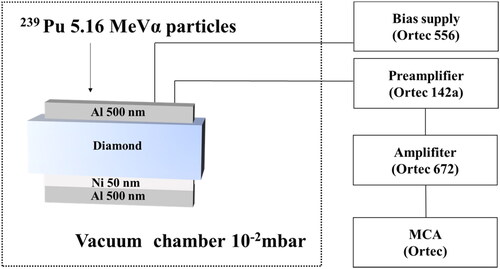
The quality of diamond crystal was measured by high spectral resolution micro-Raman and Photoluminescence (PL) spectrum (inVia Qontor) produced by Renishaw, with laser wavelength of 532 nm. The substitution of nitrogen impurities in diamond were tested by EPR (EMXplus-9.5/12) produced by Bruker. Synchrotron radiation X-ray white-beam topography (XRT) was used to directly observed the dislocation in diamond in the Beijing Synchrotron radiation Facility (BSRF). The time of flight (TOF) (DUV-PL) was tested by deep ultraviolet laser photoluminescence spectrometer independently developed by Institute of Semiconductors CAS with laser energy of 3 μJ, repetition frequency of 60 Hz, pulse width 1.3 ns. In the vacuum chamber (10−2 mbar), a pulse height analyzer composed of charge sensitive preamplifier (Ortec 142a), spectral amplifier (Ortec 672), multichannel analyzer (MCA Ortec 927) and voltage supply device (Ortec 556) were used to analyze the pulse height from 239Pu source with energy of 5.16 MeV α particle.
3. Results and discussion
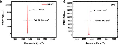
showed the Raman spectra of two samples fitted by Gauss function. The Raman characteristic peaks and their full width at half maximum (FWHM) of HPHT diamond and CVD diamond were 1333.24 cm−1 and 1333.43 cm−1, 3.68 cm−1 and 3.62 cm−1, respectively. The stress (P) in the diamond samples can be expressed as P = Δν/k. Where Δν is the displacement of Raman characteristic peak of single crystal diamond relative to unstressed Raman peak. k has been measured as 1.9 cm−1/GPa. The Raman displacement of natural synthetic diamond at room temperature was 1332.5 ± 0.2 cm −1 [Citation15,Citation16]. In this study, the stress in the HPHT diamond and CVD diamond were -0.39 and -0.49 GPa, respectively, showing the relatively high stress in the CVD diamond due to the growth stress. From the spectra, the well-known D peak around 1350 cm−1 and G peak around 1580 cm−1 originating from the disordered carbon and graphite, respectively, were not observed.
Figure 2. Laser Raman spectra of the single crystal (a) HPHT diamond and (b) CVD diamond excited at 532 nm.
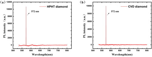
The samples were characterized by PL spectrometer with a laser of 532 nm. The characterization results are shown in . Apart from the diamond Raman peak at 572 nm, no features have been observed in HPHT diamond, indicating no inclusion was incorporated. For CVD diamond, there was no common NV defect centers at 575 nm, 638 nm and SiV- peak at 737 nm. 325 nm laser had also been used to characterize the impurity of both HPHT and CVD diamond. No peaks of N3 (415 nm) or N2 (478 nm) were observed, showing the high-purity diamond and proving the effectiveness of plasma purification technology [Citation17]. In order to calculate the nitrogen impurity in diamond without damage, we used the EPR to characterize the concentration of substituted nitrogen (NS) in diamond quantitatively.
Figure 3. Photoluminescence spectra of (a) HPHT diamond and (b) CVD diamond excited by 532 nm laser.
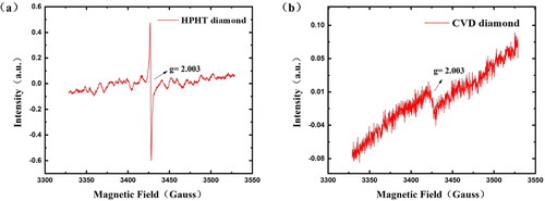
EPR spectroscopy provides a more accurate insight into the presence and content of nitrogen impurities in the diamond. The EPR spectra of the HPHT diamond and CVD diamond were shown in . The obtained g factor at 2.003 is consistent with NS centers [Citation18]. By integrating the EPR spectrum using a Gaussian function [Citation19]. The contents of NS impurities in HPHT diamond and CVD diamonds were estimated to be 20.2 ppb and 2.1 ppb, respectively. It shows the very low concentration in the CVD diamond compared with the several tens ppb in HPHT diamond. It is worth noting that the synthetic CVD diamond shows the comparable value of Ns concentration with that of the electronic-grade diamond reported by Element Six [Citation20].
Figure 4. Electron paramagnetic resonance spectra of (a) HPHT diamond and (b) CVD diamond.
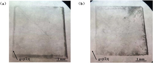
Dislocation is another important defect to affect the performance of diamond detectors. However, it is hard to characterize the dislocation density accurately. XRT is an effective non-destructive method to investigate dislocations in crystal, which can intuitively analyze the two-dimensional distribution of dislocation in the material [Citation21]. In the XRT image, the threading dislocations (TDs) from the upper surface to the lower surface of the crystal become black spots, and the transverse dislocations appear as black lines [Citation22]. TDs constitute an important issue that is still holding back the wide adoption of diamond by generating optical birefringence. showed X-ray topography images of HPHT diamond and CVD diamond. HPHT diamond was colorless and transparent and under the X-ray radiation showing there are fewer dislocations in HPHT diamond. Most areas of CVD diamond show low dislocations, but there were some aggregated dislocations at the edges, which may be related to the plasma edge effect during the growth process, promoting the growth of the non-homoepitaxial diamond [Citation23].
Figure 5. X-ray topography images of (a) HPHT diamond and (b) CVD diamond.
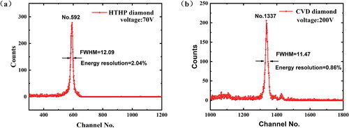
After packaging the detector, the alpha particle detection performance of detectors was characterized using a 239Pu source. Energy resolution is an important parameter for nuclear detectors in the measurement of energy spectrum, which represents the ability to distinguish similar energy spectral lines. The ratio of the FWHM to the center energy peak of the spectral line is experimentally defined as the energy resolution [Citation24]. When radiation enters the sensitive volume of a diamond sample, it will generate a certain number of electron-hole pairs. These electrons and holes start to move under the applied electric field, until they are collected by the electrodes. According to the Shockley–Ramo theorem, this current can be processed with appropriate pulse processing electronics to obtain the pulse height spectrum of the radiation [Citation25]. showed the typical pulse height spectra of diamond detectors irradiated from 239Pu source with 5.16 MeV. At 70 V, the energy resolution was 2.04% for HPHT diamond. For CVD diamond, at 200 V, the energy resolution of particles was 0.86%. Both HPHT diamond and CVD diamond showed high energy resolution characteristics.
Figure 6. Energy spectra of diamond detectors (a) HPHT diamond and (b) CVD diamond.
The saturated charge collection efficiency (CCE) of diamond detectors were obtained by comparing it with a standard silicon detector and shown in . The energy spectrum was measured under the irradiation of alpha particles at the energy of Eα. If the gain of the amplifier was Gdiamond at this time, the number of channels obtained was Chdiamond, as shown in EquationEq. (1)(1)
(1) , then the number of channels measured by the standard silicon detector under the gain of GSi was ChSi, as shown in EquationEq. (2)
(2)
(2) , where WSi was the average ionization energy of silicon and Wdiamond was the average ionization energy of diamond. Generally, the CCE of the standard silicon detector was 100%, and CCEdiamond can be expressed as EquationEq. (3)
(3)
(3) [Citation26].
(1)
(1)
(2)
(2)
(3)
(3)
Figure 7. CCE of carriers in the diamond detectors (a) HPHT diamond and (b) CVD diamond.
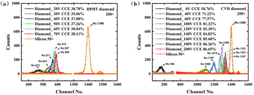
The characteristic peak in the standard silicon detector for 5.16 MeV alpha particle was observed at channel No. 1396. The average ionization energies of silicon and diamond are 3.62 eV and 13.1 eV, respectively [Citation27]. During the test, the gain of diamond detectors and silicon detector were 200 times and 50 times, respectively. With the increase of applied voltage, the CCE of electron for HPHT diamond showed a maximum value of 38.11% at 70 V. For CVD diamond, at 200 V, the CCE reached the maximum value of 86.65%. At 0 voltage, the CVD diamond detector achieved response of α and the CCE was 10.76%. Although CVD diamond is an element semiconductor, during the growth of CVD, a large number of defect centers are formed inside the material. These defects capture centers form a strong built-in electric field within the device, known as polarization effect. Therefore, even at a bias of 0 V, this built-in electric field can collect the charge carriers generated by the rays, forming an energy peak at 0 V. The polarization effect of diamond is an inherent defect in materials [Citation28,Citation29]. If taking the electrode loss for consideration, the CCE of almost 90% will be obtained. The CCE could be expressed by Hecht equation as [Citation30]
(4)
(4)
Where μτ is the product of carrier mobility and lifetime, E is the electric field strength, d is the distance between two electrodes. showed CCE curves of HPHT diamond and CVD diamond fitted according to Hecht equation. The μτ product of HPHT diamond and CVD diamond were 1.2 × 10⁻⁵ cm2V−1and 3.5 × 10⁻⁵ cm2V−1, respectively.
Figure 8. CCE curves of (a) HPHT diamond and (b) CVD diamond fitted according to Hecht equation.
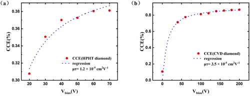
Figure 9. Time-of-Flight spectra for diamond (a) HPHT diamond (b) CVD diamond.
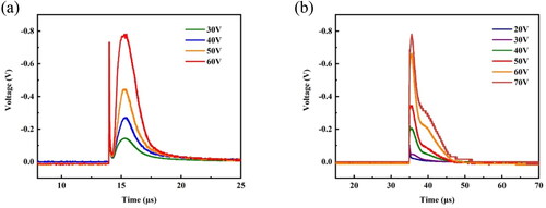
In order to further research the performance differences between HPHT diamond detector and CVD diamond detector. TOF was tested on HPHT diamond and CVD diamond to investigate the carrier transport characteristics in diamond. Ns impurities in HPHT diamond can form deep impurity level at Ec-1.7 eV [Citation31,Citation32]. Nitrogen impurity level had a trapping effect on charge carriers, causing the signal of TOF decrease to zero earlier. The time obtained from the signal was no longer the time when the charge carriers moved to the opposite electrode. When the voltage was applied, the captured charge carriers de-trapped and formed new signal. For CVD diamond, the dislocation density was higher than HPHT diamond. From the Figure 9 (b), the dislocation density mainly affected the shape of the signal top. If there was no space charge effect, the charge carriers were subjected to a constant electric field. When the charge carriers were subjected to a changing electric field, their velocity also changed and was no longer constant. Due to the presence of an internal electric field formed by the space charge in the opposite direction to the external electric field, the effect of the electric field on the charge carriers was reduced. The carrier transport velocity decreased and the decline time had a long tail band [Citation33,Citation34].
Generally, the factors that typically affect the energy resolution of nuclear detectors include statistical fluctuations in electron hole pairs generated by incident radiation within the detector, the electronic noise of the test system, the energy loss caused by non-sensitive regions in the detector structure, and the energy loss caused by the collision of incident particles [Citation35]. The energy resolution of HPHT diamond and CVD diamond detectors were 2.04% and 0.86% respectively, showing high energy resolution. However, the HPHT single crystal diamond showed less than 40% of CCE under the applied voltage from 20 V to 70 V. Under ideal conditions, all charges generated by an impinging ion are measured as it drifts towards the electrodes. However, charge carriers can be trapped or recombined before reaching the electrode resulting in a decreased CCE. Any distortion to the periodicity of the diamond lattice or different impurities, influences the electronic and transport properties of the material and possibly creates traps for the generated charge carriers. The impurity content of Ns in HPHT diamond was one order of magnitude higher than CVD diamond. The deep impurity level formed by nitrogen impurities had a trapping effect on carriers. The XRT results showed that the dislocation density in HPHT diamond was lower than that in CVD diamond, Dislocation might play an important role in the formation of built-in electric fields in diamond so that CVD diamond detector exhibited response to α particles at zero voltage. The CCE is related to the carrier mobility and lifetime. The deep impurity level formed by nitrogen impurity had trapping effect on the carrier which will reduce the μτ product. The μτ product of HPHT diamond and CVD diamond were 1.2 × 10⁻⁵ cm2V−1and 3.5 × 10⁻⁵ cm2V−1, respectively, which were the typical value in the reported diamond detectors. Furthermore, the charge carriers in the traps could be recombined, thus leading to a lower detector CCE [Citation36].
4. Conclusions
The performance of diamond detectors prepared by CVD diamond was compared with the original HPHT substrate. By using chemical vapor deposition combining the chamber design and the plasma purifying technology, synthetic high-purity single crystal diamond was epitaxially grown. The trace impurity of substitutional nitrogen was characterized by EPR. It showed the very low concentration in the CVD diamond (2.1 ppb). The energy resolution of HPHT and CVD diamond detectors were 2.04% and 0.86%, respectively. Based on Schottky contact and defect regulation, at 0 voltage, the CVD diamond detector achieved response to α particles and the CCE was 10.76%. Under positive voltage, the CCE of HPHT and CVD diamond detectors were 38.11% and 86.65%, respectively. The deep level trapping effect of Ns impurities on charge carriers resulted in low CCE of HPHT diamond detector. The spatial polarization effect caused by dislocation led to the formation of an internal electric field, which is the main reason affecting the charge carriers transport in CVD diamond.
Authors’ contributions
Lianxi Mu, Tingting Hu, Jinlong Liu, Zhifu Zhu, Runlong Gao and Linyue Liu performed the experiments and wrote the article. Liangxian Chen, Junjun Wei, Yuting Zheng, Xiaoping Ouyang and Chengming Li helped to analyze the data and conceive the framework of this paper. All the authors commented on the final paper.
Disclosure statement
No potential conflict of interest was reported by the authors.
Additional information
Funding
Notes on contributors
Lianxi Mu
Lianxi Mu is a master student, Jinlong Liu and Chengming Li are professors in University of Science and Technology.
Zhifu Zhu
Zhifu Zhu is a professor in Zhengzhou University of Technology.
References
- Bossini E, Minafra N. Diamond detectors for timing measurements in high energy physics. Front Phys. 2020;8:1.
- Trischuk W, Artuso M, Bachmair F, et al. Diamond particle detectors for high energy physics. Nuclear Particle Phys Proc. 2016;273:1023–8.
- Pompili F, Esposito B, Marocco D, et al. Radiation and thermal stress test on diamond detectors for the radial neutron camera of ITER. Nucl Instrum Methods Phys Res Sect A. 2019;936:62–64.
- Bassi G, Bosisio L, Cristaudo P, et al. Calibration of diamond detectors for dosimetry in beam-loss monitoring. Nucl Instrum Methods Phys Res Sect A. 2021;1004:165383.
- Kim M, Seo JH, Singisetti U, et al. Recent advances in free-standing single crystalline wide band-gap semiconductors and their applications: gaN, SiC, ZnO, β-Ga2O3, and diamond. J Mater Chem C. 2017;5(33):8338–8354.
- Marczewska B, Kupriyanov I, Nowak T, et al. A study of radiation dosimeters based on synthetic HPHT diamond. Diamond Relat Mater. 2007;16(2):191–195.
- Tallaire A, Brinza O, Mille V, et al. Reduction of dislocations in single crystal diamond by lateral growth over a macroscopic hole. Adv Mater. 2017;29(16):1604823.
- Makoto K, Ryuichi M, Satoshi M, et al. Synchrotron X-ray topography of dislocations in high-pressure high-temperature-grown single-crystal diamond with low dislocation density. Appl Phys Express. 2014;7:125501.
- Sumiya H, Tamasaku K. Large Defect-Free synthetic type IIa diamond crystals synthesized via high pressure and high temperature. Jpn J Appl Phys. 2012;51(9R):090102.
- Sergey VC, Alexey VC, Sergey AT, et al. High-pressure high-temperature single-crystal diamond type IIa characterization for particle detectors. Physica Status Solidi. 2020;217(8):1900888.
- Ohmagari S, Yamada H, Tsubouchi N, et al. Toward high‐performance diamond electronics: control and annihilation of dislocation propagation by metal‐assisted termination. Physica Status Solidi (a). 2019;216(21):1900498.
- Su JJ, Li YF, Ding MH, et al. A dome-shaped cavity type microwave plasma chemical vapor deposition reactor for diamond films deposition. Vacuum. 2014;107:51–55.
- Liu JL, Lin LZ, Zhao Y, et al. Homoepitaxial growth of single crystal diamond in the purified environment by active O atoms. Vacuum. 2018;155:391–397.
- Mu LX, Su K, Hu TT, et al. High charge collection efficiency detector based on plasma purified high-quality diamond. Diamond Relat Mater. 2022;130:109527.
- Kone S, Schneider H, Isoird K, et al. An assessment of contact metallization for high power and high temperature diamond schottky devices. Diamond Relat Mater. 2012;27–28:23–28.
- Bergman L, Nemanich RJ. Raman and photoluminescence analysis of stress state and impurity distribution in diamond thin films. J Appl Phys. 1995;78(11):6709–6719.
- Ganesan K, Ajikumar PK, Srivastava SK, et al. Structural, raman and photoluminescence studies on nanocrystalline diamond films: effects of ammonia in feedstock. Diamond Relat Mater. 2020;106:107872.
- Lee C, Cheng J, Yiu YC, et al. Correlation between EPR spectra and coloration of natural diamonds. Diamond Relat Mater. 2020;103:107728.
- Zhang ZF, Lin CN, Yang X, et al. Wafer-sized polycrystalline diamond photodetector planar arrays for solar-blind imaging. J Mater Chem C. 2022;10(16):6488–6496.
- Tallaire A, Mille V, Brinza O, et al. Thick CVD diamond films grown on high-quality type IIa HPHT diamond substrates from new diamond technology. Diamond Relat Mater. 2017;77:146–152.
- Shikata S, Miyajima K, Akashi N. Analysis method of diamond dislocation vectors using reflectance mode X-ray topography. Diamond Relat Mater. 2021;118:108502.
- Kato Y, Umezawa H, Yamaguchi H, et al. Structural analysis of dislocations in type-IIa single-crystal diamond. Diamond Relat Mater. 2012;29:37–41.
- Zhao Y, Guo YZ, Lin LZ, et al. Comparison of the quality of single-crystal diamonds grown on two types of seed substrates by MPCVD. J Cryst Growth. 2018;491:89–96.
- Su K, Wang H, He Q, et al. A large gain and high resolution diamond radiation detector with Au/hydrogen termination ohmic contact IEEE Electron Device Lett. 2022;43(3):454–457.
- Zamboni I, Pastuovic Z, Jakšic M. Radiation hardness of single crystal CVD diamond detector tested with MeV energy ions. Diamond Relat Mater. 2013;31:65–71.
- Naaranoja T, Golovleva M, Martikainen L, et al. Space charge polarization in irradiated single crystal CVD diamond. Diamond Relat Mater. 2019;96:167–175.
- Su K, Ren Z, Zhang J, et al. High performance hydrogen/oxygen terminated CVD single crystal diamond radiation detector. Appl Phys Lett. 2020;116(9):092104.
- Ramos MR, Crnjac A, Provatas G, et al. Characterization of ion beam induced polarization in scCVD diamond detectors using a microbeam probe. Nucl Instrum Methods Phys Res Sect B. 2021;504:21–32.
- Zhu ZF, Zou JJ, Sun ZJ, et al. Graded composition and doping p-i-n AlxGa1−xAs/GaAs detector for unbiased voltage operation. Nucl Sci Tech. 2022;33(7):85.
- Kasap S, Ramaswami KO, Kabir MZ, et al. Corrections to the hecht collection efficiency in photoconductive detectors under large signals: non-uniform electric field due to drifting and trapped unipolar carriers. J Phys D Appl Phys. 2019;52(13):135104.
- Schreck M, Ščajev P, Träger M, et al. Charge carrier trapping by dislocations in single crystal diamond. J Appl Phys. 2020;127(12):125102.
- Lohstroh A, Sellin PJ, Wang SG, et al. Effect of dislocations on charge carrier mobility-lifetime product in synthetic single crystal diamond. Appl Phys Lett. 2007;90(10):102111.
- Deferme W, Mackova A, Haenen K, et al. Surface states and photo-induced charge transfer on oxygen-terminated chemical vapor deposition diamond. J Appl Phys. 2011;109(6):063701.
- Valentin A, Tardieu A, Mille V, et al. Polarization effect on time-of-flight measurements performed on a CVD diamond single crystal. Phys Status Solidi A Appl Mater Sci. 2015;212(11):2636–2640.
- Shimaoka T, Kaneko JH, Sato Y, et al. Fano factor evaluation of diamond detectors for alpha particles. Phys Status Solidi (a). 2016;213(10):2629–2633.
- Cosic D, Provatas G, Jaksic M, et al. Charge collection efficiency of scCVD diamond detectors at low temperatures. Diamond Relat Mater. 2022;127:109184.