Abstract
We review our recent work on spatial inhomogeneity of the electronic states in the strongly correlated molecular conductors κ-(BEDT-TTF)2X. Spatial mapping of infrared spectra (SMIS) is used for imaging the distribution of the local electronic states. In molecular materials, the infrared response of the specific molecular vibration mode with a strong electron–molecular vibration coupling can reflect the electronic states via the change in the vibration frequency. By spatially mapping the frequency shift of the molecular vibration mode, an electronic phase separation has been visualized near the first-order Mott transition in the bandwidth-controlled organic conductor κ-(BEDT-TTF)2Cu[N(CN)2]Br. In addition to reviewing SMIS of the phase separation, we briefly mention the electronic and optical properties of κ-(BEDT-TTF)2X.
Introduction
Local electronic states of sub-nanometer to sub-millimeter sizes have attracted much attention recently in the fields of strongly correlated electron materials, low-dimensional materials, cluster materials and so on. The development of scanning tunneling and atomic force microscopes has greatly contributed to the progress of such local electronic state measurements. The probe microscopy is very powerful for observing the local surface structure and electronic states at atomic and molecular scales [Citation1–3]. However, larger-scale inhomogeneities resulting from intrinsic microscopic or extrinsic origins such as surface effects are also important for understanding macroscopic phenomena including electronic resistivity and magnetization.
Basic spatial mapping can be performed using conventional optical microscopes probing the difference in the local reflectivity of visible light. Using the characteristic optical response of the materials, which depends on the manner of coupling to light, we can spatially study the chemical, structural and electronic properties. For example, infrared and Raman microscopes are commercially available and widely used [Citation4, Citation5]. In the case of infrared spectroscopy and the imaging of molecular conductors having correlated electrons, which we are interested in here, we can obtain the information about the low-energy charge response, as well as molecular vibrational properties. Furthermore, whereas scanning probe microscopy is restricted to the surface, infrared light can probe much deeper regions of the sample. We have studied the infrared optical properties of the organic dimer Mott system κ-(BEDT-TTF)2X, where BEDT-TTF is the donor molecule bis(ethylenedithio)-tetrathiafulvalene and X is an anion molecule [Citation6]. This family of compounds is known as a strongly correlated electron system [Citation7–9]. We found that the characteristic molecular vibration modes of BEDT-TTF molecules were sensitive to the carrier localization on the BEDT-TTF dimer site. The frequency of this vibration shifted with the degree of charge localization, which is known as the electron–molecular vibration (EMV) coupling [Citation10, Citation11]. The sensitive shift of the molecular vibration in the infrared spectra was useful for probing the distribution of the electronic states. The latter was performed with spatial mapping of infrared spectra (SMIS)Footnote3, which is a powerful method for investigating the spatial distribution of the electronic states over sub-millimeter areas. By performing SMIS on κ-(BEDT-TTF)2X using synchrotron radiation, we have found a macroscopic electronic inhomogeneity of the Mott insulating region and the superconducting region in κ-(BEDT-TTF)2Cu[N(CN)2]Br very close to the border of the Mott transition [Citation12, Citation13].
In this article, we review the visualization of the spatial phase separation observed in the organic dimer Mott system κ-(BEDT-TTF)2X [Citation12–15]. To achieve sufficient spatial resolution, a synchrotron is used as the infrared light source [Citation16]. In the following sections, we present the basic concepts of the organic dimer—Mott insulators, their electronic and infrared optical properties, the method of imaging the electronic states by SMIS combined with synchrotron radiation, and the electronic phase separation near the Mott transition in κ-(BEDT-TTF)2Cu[N(CN)2]Br.
Quasi two-dimensional strongly correlated electron system κ-(BEDT-TTF)2X
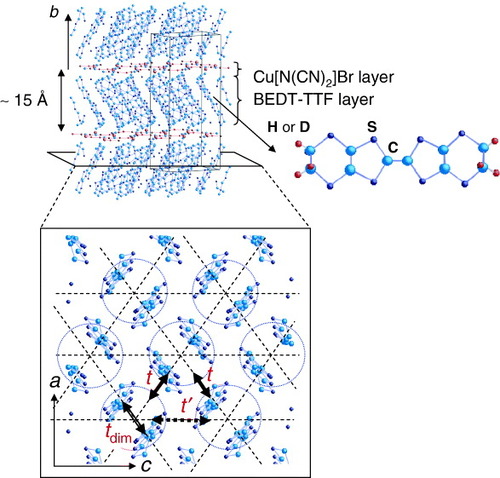
Organic charge-transfer salts based on the donor molecule bis(ethylenedithio)-tetrathiafulvalene, abbreviated to BEDT- TTF or ET, have been recognized as one of the most highly correlated electron systems [Citation17]. Among them, κ-(BEDT-TTF)2X with X=Cu(NCS)2 or Cu[N(CN)2]Y (Y=Br or Cl), Cu2(CN)3, etc, has attracted considerable attention from the viewpoint of its strongly correlated quasi- two-dimensional electron systems, because the native quarter- filled band is modified to an effective half-filled band by the strong dimer structure consisting of two BEDT-TTF molecules [Citation7–9]. The crystal structure of the organic superconductor κ-(BEDT-TTF)2Cu[N(CN)2]Br and the schematic two-dimensional network of the BEDT-TTF dimers are shown in figure . The two-dimensional conduction plane consists of BEDT-TTF molecular dimers, which form an anisotropic triangular lattice. The intradimer transfer energy tdim is larger than the interdimer transfer energies t and t′. The anisotropy of the triangular lattice changes with the t′ /t ratio which ranges from 0.7 in κ-(BEDT-TTF)2Cu[N(CN)2]Br to 1.1 in κ-(BEDT-TTF)2Cu2(CN)3 [Citation18, Citation19]. In this strongly correlated electronic system, several electronic phases appear and the transitions between these phases are controlled by the applied pressure and the slight chemical substitution of donor and anion molecules, which change the conduction band width W∼4t with respect to the effective Coulomb repulsion Ueff of a dimer. The value of Ueff can be estimated simply as , where U is the Coulomb energy of the BEDT-TTF molecule [Citation7–9]. This equation yields Ueff∼0.3 eV for U∼1 eV and tdim∼0.25 eV. This value of Ueff is comparable to the bandwidth W∼4t and suggests that correlation effects are important.
Figure 1 Crystal structure of κ-(BEDT-TTF)2Cu[N(CN)2]Br. The two-dimensional conduction plane consists of BEDT-TTF molecular dimers, which form the anisotropic triangular lattice. The intradimer transfer energy tdim is larger than the interdimer transfer energies t and t′.
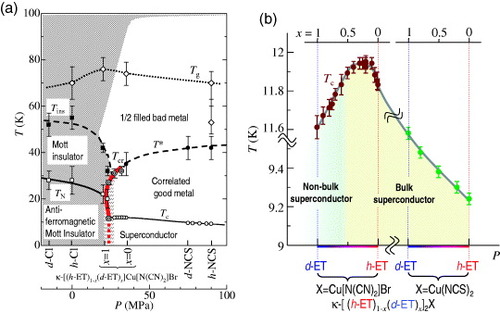
The electronic phase diagram of κ-(BEDT-TTF)2X with the anisotropic triangular dimer lattice is shown in figure (a) [Citation20]Footnote4. The first-order metal–insulator Mott transition (thick red curve) divides the pressure–temperature plane of the phase diagram into the superconducting and antiferromagnetic Mott insulating phases. The Mott transition curve is extended to a higher temperature above the superconducting transition temperature Tc and antiferromagnetic long-range ordering temperature TN [Citation21], and is terminated at the critical end point Tcr≃40 K [Citation22]. From Tcr on both weak and strong correlation sides in the phase diagram, the T∗ line and the bad metal–insulator line Tins are elongated. At temperatures above Tcr, T∗ and Tins, the bad metallic state with the effective half-filled band exists over a wide range of correlation strengths which can be tuned by pressure and by the substitution of an anion. On the weak correlation side from Tcr, the bad metal changes to a correlated good metal at T∗ and then becomes superconducting. On the strong correlation side, the bad metal becomes a Mott insulator at Tins and then becomes an antiferromagnetic Mott insulator at TN. Applied magnetic field suppresses the superconducting phase and extends the Mott insulating phase to the good-metal phase [Citation26, Citation27]. Thus, the κ-(BEDT-TTF)2X family was considered a bandwidth-controlled Mott system in contrast to the filling-controlled system in inorganic perovskites, such as high-Tc copper oxides. Note that the above discussion of the phase diagram applies to the anisotropic triangular lattice system κ-(BEDT-TTF)2X with X = Cu(NCS)2, Cu[N(CN)2]Y (Y= Br or Cl). κ-(BEDT-TTF)2Cu2(CN)3, which has a nearly triangular lattice, is suggested to have a spin liquid ground state instead of an antiferromagnetic order owing to the spin frustration [Citation28, Citation29], and its nature is being actively investigated both experimentally [Citation30, Citation31] and theoretically [Citation32, Citation33].
Figure 2 (a) Electronic phase diagram of κ-(BEDT-TTF)2X. The horizontal axis corresponds to the chemical and physical pressures. The thick red curve is the first-order Mott transition curve. (b) Variation of Tc in κ-[(h-ET)1−x(d-ET)x]2X (X=Cu[N(CN)2]Br and Cu(NCS)2) with the substitution ratio x in the deuterated BEDT-TTF molecule (from [Citation41]).
In addition to the strong electronic correlation, characteristic flexibility in the molecules and crystal lattices plays an important cooperative role in modulating the electronic properties in κ-(BEDT-TTF)2X. In particular the terminal ethylene groups of BEDT-TTF molecules undergo a conformational order–disorder glass transition at Tg≃80 K [Citation34, Citation35]. The degree of disorder is expected to change with the cooling rate at Tg. Faster cooling may induce disorder in the terminal ethylene groups at low temperatures. This type of disorder at the molecular scale might be related to the pinning effect of vortices [Citation38, Citation39] and the quasi-particle scattering. Moreover such a cooling rate effect has been discussed in terms of the change in the correlation strength Ueff/W, which can switch the ground state near the Mott transition [Citation40].
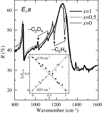
To control the electron correlation in κ-(BEDT-TTF)2X, we attempted to grow crystals with the BEDT-TTF molecules (h-ET) partially substituted with the deuterated molecules (d-ET). Single crystals of κ-[(h-ET)1−x(d-ET)x]2 Cu[N(CN)2]Br were grown by the standard electrochemical oxidation method [Citation41]. The typical dimensions of the samples were ∼1×1×0.2 mm3. The substitution ratio x denotes the nominal mole ratio to the fully deuterated BEDT-TTF molecule. We verified the actual substitution by measuring the intensity of the molecular vibrational mode of the terminal ethylene groups, which was observed in the mid-infrared region (the so-called fingerprint region). Figure shows an example of the reflectivity spectra for the E||a-axis in the fingerprint region of κ-[(h-ET)1−x(d-ET)x]2Cu[N(CN)2]Br at 300 K. In the x=0 sample, the vibration modes for the terminal ethylenes can be seen as sharp peaks. The dips are due to the overlapping Fano-type antiresonances on the broad peak of the ν3(ag) mode, which is a symmetric stretch of the central group of BEDT-TTF moleculesFootnote5. Additional vibrations for the deuterated terminal ethylenes appear at lower frequencies in the samples enriched with deuterated BEDT-TTF moleculesFootnote6. To obtain the dependence of the intensity of the vibration modes in ethylene and deuterated ethylene on the nominal substitution ratio x, we compared the reflectivity spectra in the samples with various values of x to that for x=1. Lorentz-type vibrational structures related to the terminal ethylenes and deuterated ethylenes only appeared in the difference spectra. The intensity of the Lorentz-type spectra should be proportional to the oscillator number, which corresponds to the actual substitution ratio between the hydrogenated and deuterated BEDT-TTF molecules. The intensity of the terminal ethylene vibrations decreases linearly with increasing x as shown in the inset of figure , while the intensity of the vibration mode for the deuterated terminal ethylenes increases by way of compensation.
Figure 3 Reflectivity spectra for E||a-axis in κ-[(h-ET)1−x(d-ET)x]2Cu[N(CN)2]Br at 300 K. The intensity of the molecular vibration modes for the terminal ethylenes of the BEDT-TTF molecules changes with the substitution ratio x. The inset indicates the linear relation between the normalized intensity of the terminal ethylene (1170 cm−1) and deuterated ethylene (1025 cm− 1) modes and the nominal substitution ratio x.
The substitution dependences of the macroscopic phase diagram and the superconducting properties have been examined (figures (a) and (b)). The full volume of the superconductivity can be observed in the range of x= 0–0.5 when the samples are cooled slowly. In this substitution range, Tc is increased slightly by about 0.1 K when x increases from 0 to ∼0.1. Then Tc remains constant at 11.9 K for x up to ∼0.5. Above x=0.5, however, the superconducting volume fraction decreases to ∼40 vol% for x=1; this value strongly depends on the cooling condition. Concurrently with the reduction of the superconducting volume fraction, Tc decreases from 11.9 K at x=0.5 to 11.6 K at x=1. The remaining portion of the superconducting part may be the antiferromagnetic Mott insulator; in this case, the magnetic impurity effect resulting from such a coexistence of two phases may reduce Tc. This simple substitution allows to control the bandwidth continuously at ambient pressure with minimal disorder effect. In rapid cooling, however, both the superconducting volume fraction and Tc decrease considerably with x. This superconducting volume fraction deduced from the magnetization measurements will be shown in figure together with the present optical imaging results.
Inhomogeneous electronic states have been suggested near the first-order metal–insulator transition in artificially bandwidth controlled κ-(BEDT-TTF)2Cu[N(CN)2]Br on the basis of 13C nuclear magnetic resonance experiments [Citation47]. Below the characteristic temperature T∗, 13C nuclear magnetic resonance lines fall into two groups, indicating metallic and antiferromagnetic insulating behaviors. The results imply that those two phases coexist spatially and statically. Subsequent transport experiments have also suggested the coexistence of those two phases at low temperatures [Citation48]. It is very important to obtain detailed spatial information, which can indicate mechanism of the macroscopic phase separation observed in this strongly correlated electronic system.
Imaging electronic states by spatial mapping of optical spectra
Infrared optical spectra of organic conductors
To obtain spatial images of the electronic states from optical measurements, we need spectra with specific structure that sensitively reflects the change in the electronic states, for example, the difference between the metallic and insulating states [Citation11]. In this section, we compare the optical spectra for the metallic and insulating states of κ-(BEDT-TTF)2X and show that the EMV-coupled modes are sufficiently sensitive to the difference in the electronic states and therefore can be used for the imaging.
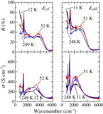
Figure shows the reflectivity (upper panels) and optical conductivity spectra (lower panels) calculated by the Kramers–Kronig transformation for the E||c-axis (left panels) and E||a-axis (right panels) of κ-(BEDT-TTF)2 Cu[N(CN)2]Br, which exhibits superconductivity at 11.6 K [Citation6]. The spectra have the following characteristic features:
a Drude peak appears only at low temperatures,
a broad mid-infrared conductivity peak exists at 3300 cm−1 for the E||c-axis and 2200 cm−1 for the E||a-axis and
the molecular vibrational modes of BEDT-TTF are superimposed on the electronic background spectra at approximately 1000–1500 cm−1.
Figure 4 Reflectivity (upper panels) and optical conductivity spectra (lower panels) of κ-(BEDT-TTF)2Cu[N(CN)2]Br for E||c-axis (left panels) and E||a-axis (right panels) (from [Citation6]).
The Drude part in the low-frequency region may be a good indicator for the mapping measurements. However, the far-infrared measurements on small samples are difficult because of the limitation by the optical diffraction. The mid-infrared bands are attributed to the interband transitions of the dimer bands and Mott–Hubbard bands [Citation49]. This feature of these bands also reflects the electronic states. Insulating materials (for example, κ-(BEDT-TTF)2 Cu[N(CN)2]Cl) show a large enhancement of the broad mid-infrared absorption peaks instead of the Drude part in the low-frequency region. However, such broad spectral features are difficult to use for mapping.
The change in the electronic states in these salts is reflected in the totally symmetric internal vibration ν3(ag) mode of the BEDT-TTF molecule through the EMV coupling [Citation10, Citation11] (see footnote Footnote5). The symmetric ν3(ag) mode becomes visible in the infrared spectra owing to the large EMV coupling (figure ). The infrared frequency νIR is expected to be lower than the bare phonon frequency ν0 (≃νR: Raman frequency) when the transfer integral tdim for hopping between molecules within the dimer is larger than ν0 (≃νR). The peak of the ν3(ag) mode should shift to a lower frequency in the insulating state, while it exhibits the opposite behavior in the metallic state.
Figure 5 Schematic figure for electron–molecular vibration (EMV) coupling in BEDT-TTF molecular dimer and the EMV- coupled totally symmetric mode in the BEDT-TTF molecule.
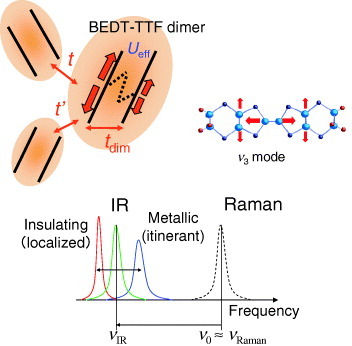
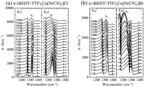
Figure shows the optical conductivity at frequencies near 1300 cm−1 for (a) κ-(BEDT-TTF)2Cu[N(CN)2]Cl and (b) κ-(BEDT-TTF)2Cu[N(CN)2]Br [Citation6]. The measurements for both samples were performed using a slow cooling rate of about 0.4–0.5 K min−1. The sharp peaks in the spectra are assigned to the vibrational modes as follows. The peaks at approximately 1170 and 1270–1290 cm−1 are assigned to ν67 and ν5 modes, respectively, both of which involve the CH2 group [Citation42]. The peak at 1380–1390 cm−1 is assigned to ν45 [Citation42] (see footnote Footnote6). The frequencies of these peaks do not change significantly with temperature. The peaks at 1320–1330 cm−1 for the E||c-axis and 1250–1270 cm−1 for the E||a-axis, which are assigned to the ν3(ag) mode, shift to lower frequencies below 50–60 K in κ-(BEDT-TTF)2Cu[N(CN)2]Cl, whereas they shift to higher frequencies below about 30–40 K in κ-(BEDT-TTF)2 Cu[N(CN)2]BrFootnote7. In view of such changes in the vibration frequency of the ν3(ag) mode, let us consider its relation with the electronic states. A large negative frequency shift from the bare phonon frequency, which appears with a small gradual background shift to higher frequencies probably due to the lattice contraction [Citation6, Citation43], is observed below Tins. At those temperatures, the carriers are localized at the dimer sites and the electrical conductivity is low. The larger and sharper peak of the ν3(ag) mode also demonstrates the localization of a carrier (one hole) at each dimer; thus, the system has become the Mott insulating state. On the other hand, the positive frequency shift below T∗ indicates that the carriers on the dimers exhibit itinerant behavior in the superconducting salt.
Figure 6 Optical conductivity spectra near 1300 cm−1 of (a) κ-(BEDT-TTF)2Cu[N(CN)2]Cl and (b) κ-(BEDT-TTF)2Cu[N(CN)2]Br. The spectra in (a) and (b) are shifted by 400 and 150 S cm−1, respectively (from [Citation6]).
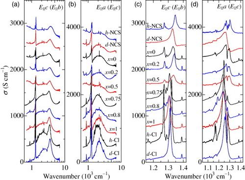
A change in the ν3(ag) mode also appears with a modification of the bandwidth. Figure shows the optical conductivity spectra of κ-(BEDT-TTF)2X at 10 K. The spectra in figures (a)–(d) from the top to bottom correspond to κ-(h-BEDT-TTF)2Cu(NCS)2 (h-NCS), κ-(d-BEDT-TTF)2 Cu(NCS)2 (d-NCS), κ-[(h-ET)1−x(d-ET)x]2Cu[N(CN)2]Br with x= 0, 0.2, 0.5, 0.75, 0.8 and 1, κ-(h-BEDT-TTF)2 Cu[N(CN)2]Cl (h-Cl) and κ-(d-BEDT-TTF)2Cu[N(CN)2]Cl (d-Cl). In comparison to the phase diagram shown in figure (a), the bandwidth in these materials decreases in order from the top to bottom curves in figures (a)–(d). This order is opposite to that of the electron correlation strength Ueff/W. The materials having strong electron correlations possess an optical conductivity gap in the low-frequency region, which indicates the Mott insulating state, whereas high conductivity due to the Drude response appears in the metallic and superconducting materials with weak electron correlations. The different spectral weight at low frequencies is compensated by transferring the weight to the mid-infrared region, in which the interband transitions take place for the dimer bands and Hubbard bands [Citation11, Citation49]. The insulators exhibit an enhancement of the interband transitions, whereas it is suppressed in metals. These drastic spectral changes occur between x=0.5 and 0.75 in κ-[(h-ET)1−x(d-ET)x]2Cu[N(CN)2]Br that corresponds to the first-order Mott transition. A distinct change in the features of the EMV-coupled ν3(ag) mode coincides with this transition as shown in figures (c) and (d). A large negative frequency shift and the enhancement of the conductivity distinguish the Mott insulating states from the metallic state. As a result, the EMV-coupled ν3(ag) mode is suitable for detecting the change in the electronic state.
Figure 7 Optical conductivity spectra of κ-(BEDT-TTF)2X at 10 K. The spectra in (a)–(d) from the top to bottom correspond to κ-(h-BEDT-TTF)2Cu(NCS)2 (h-NCS), κ-(d-BEDT-TTF)2Cu(NCS)2 (d-NCS), κ-[(h-ET)1−x(d-ET)x]2Cu[N(CN)2]Br with x= 0, 0.2, 0.5, 0.75, 0.8, and 1, κ-(h-BEDT-TTF)2Cu[N(CN)2]Cl (h-Cl) and κ-(d-BEDT-TTF)2Cu[N(CN)2]Cl (d-Cl). The spectra are shifted by 300 S cm- 1 in (a) and (c) and by 400 S cm- 1 in (b) and (d). The polarization direction in (a) and (c) is parallel to the c-axis (the b-axis for h-NCS and d-NCS) and the polarization direction in (b) and (d) is parallel to the a-axis (the c-axis for h-NCS and d-NCS).
The advantages of the molecular vibration for mapping the local electronic state by SMIS are as follows. A frequency shift of the molecular vibration can be detected with high accuracy using a Fourier transform infrared spectrometer. The frequency does not depend on the conditions of the sample surface and measurement apparatus, however scratches and steps on the surface reduce the reflectivity. In addition, the frequency is not affected by changes in the intensity of the light source and the stability of the detectors. These stability advantages are important when using synchrotron radiation and the long measuring time required for mapping experiments.
Spatial mapping of infrared spectra (SMIS) using synchrotron radiation
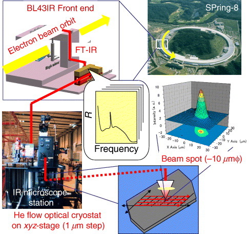
SMIS using synchrotron radiation was performed at the infrared materials science beam line BL43IR of the large synchrotron radiation facility SPring-8, Japan Synchrotron Radiation Research Institute. Figure shows a schematic experimental diagram of the setup. Infrared light was guided, in vacuum, from the storage ring to the sample using mirrors. Polarized reflectivity spectra were measured from the single-crystal surface of κ-(BEDT-TTF)2X using a Fourier transform spectrometer (Bruker, 120HR/X) equipped with a microscope, KBr beam splitter, polarizer and cooled HgCdTe detector. The infrared microscope has a set of large Schwarzschild mirrors with a precision x–y–z stage (1 μm step control). The sample and a gold mirror were fixed with conductive carbon paste on a copper sample holder which was placed at the cold head of the helium-flow cryostat. The reflectivity was obtained by comparison with that of the gold mirror at each measurement temperature. The cryostat window is made of BaF2. The mapping area was selected far from the mechanical contacts on the sample, in order to minimize strain effects due to the difference of the thermal contraction of the organic crystals, copper plate and carbon paste.
Figure 8 Schematic diagram of the spatial mapping of infrared spectra (SMIS) using synchrotron radiation at the infrared materials science beam line BL43IR of SPring-8.
Infrared synchrotron radiation is characterized by high brilliance and directionality. The infrared output of the synchrotron radiation at BL43IR, integrated up to 10 000 cm−1, is estimated as 1 mW. This value is comparable to that of conventional thermal radiation sources such as Globar [Citation50]Footnote8. However, if a Globar is used for mapping with spatial resolution ∼10 μm then the measurements would take 100–1000 times longer than when using a synchrotron.
No sample heating or degradation has been observed under the synchrotron infrared radiation so far; therefore, it has also been used for analyzing ancient cultural treasures [Citation51]. The advantage of synchrotron beams for microscopy is high brilliance originating from the small size (∼10 μm) of the source and high directionality of the radiation. Such beams can be focused to area ∼10 μm in diameter without using apertures. The latter are required for focusing conventional thermal sources (size ∼10 mm) but they strongly reduce the light intensity. The disadvantage of synchrotron radiation, however, is its instability due to low-frequency mechanical vibrations and high-frequency electron fluctuations [Citation50]. This instability leads to a lower signal-to-noise ratio compared to thermal radiation sources. To overcome this disadvantage in SMIS, it is preferable to map the frequency shift of the vibration modes rather than the intensity variation of the Drude response and the interband transitions.
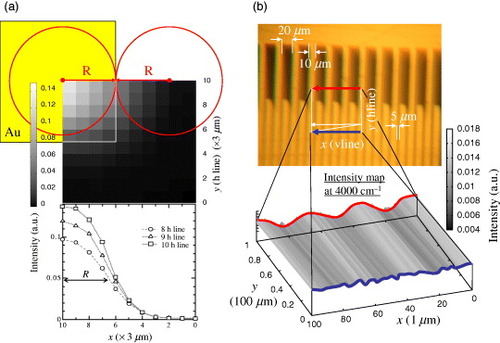
Here we derive the spatial resolution of SMIS at BL43IR, SPring-8. Figure (a) shows the reflectivity map (step 3 μm) at 4000 cm−1 for the corner of a gold mirror. This intensity map indicates the spatial resolution of SMIS ∼10 μm. We verified this spatial resolution by measuring stripes on the gold film (figure (b)). The stripes with 10 μm width are lined up with 5 or 20 μm spacing. The lower panel of figure (b) shows the intensity profile at 4000 cm−1. The 10 μm stripes can be resolved in the case of 20 μm spacing (red curve), but not in the case of 5 μm spacing (blue curve). Thus, the spatial resolution of SMIS is ∼10 μm in the mid-infrared region. This resolution is comparable to the wavelength of the infrared light at 1000 cm−1 and may be restricted by the diffraction limit. One might expect higher resolution at shorter wavelengths, but it is not, perhaps due to imperfection of the collimating optics.
Figure 9 Demonstration of the spatial resolution of SMIS at 4000 cm−1. (a) Mapping of a sharp corner of a gold mirror indicates the resolution of ∼10 μm. (b) SMIS images of the stripes on the gold film. The stripes with 10 μm width can be resolved in the case of 20 μm spacing, but not in the case of 5 μm spacing.
Macroscopic electronic phase separation observed by SMIS
Figure (a) shows the two-dimensional contour map of the reflectivity peak frequency of the ν3(ag) mode (E||a-axis) at 4 K in κ-[(h-ET)1−x(d-ET)x]2Cu[N(CN)2]Br with x= 0.6 [Citation12, Citation13]. The polarized reflectivity spectra are recorded with a beam focused to ∼ 10 μm and a step of 12 μm. The reflectivity peaks for the ν3(ag) mode are extracted and the frequencies at the peak positions are plotted as a two-dimensional contour mapFootnote9. In each pixel, bright colors (higher frequency) indicate a metallic nature and dark colors (lower frequency) indicate an insulating nature. We carefully minimized the stress and ensured good thermal of the sample as described in the previous section. Under the normal cooling condition, the samples were cooled slowly from room temperature to 4 K at a rate of about 0.4 K min−1. It took about 1 min to acquire one infrared spectrum at a spectral resolution of 2 cm−1 and 100-scan accumulation. Thus, the total measurement time to obtain one image (∼0.3×0.3 mm2) was about 8 h.
Figure 10 (a) Peak frequency contour map of the ν3 mode (E||a-axis) of κ-[(h-ET)0.4(d-ET)0.6]2Cu[N(CN)2]Br at 4 K. Bright colors (higher frequency) indicate a metallic nature and dark colors (lower frequency) indicate an insulating nature. The metal–insulator phase separation can be observed as a spatial image (from [Citation13]). (b) Reflectivity spectra along the arrow A–B in (a). (c) Intensity map of the molecular vibration mode ν5 at about 1280 cm-1 for the terminal ethylenes at T=298 K. The area of the image is the same as that in (a). No reliable reflectivity spectra for the absolute values are obtained at the positions of the blank pixels owing to the defect of the surface. (d) Normalized pixel number histogram for the intensity variation of the ν5 mode in the spatial map of κ-[(h-ET)1−x(d-ET)x]2 Cu[N(CN)2]Br for x= 0 (not shown here as a contour map) and 0.6 (a).
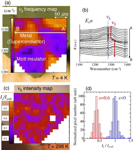
This contour map reveals metallic and insulating regions having micrometer sizes and irregular shapes. Figure (b) shows the reflectivity spectra around 1300 cm−1, which are measured along the line from A to B indicated in figure (a) with a 12 μm step. The boundary between the insulating and metallic regions is within the instrumental resolution, and there is apparently no intermediate state around the boundary. This observation indicates a macroscopic phase separation between the metal (superconductor) and insulator (Mott insulator). The sample (κ-[(h-ET)0.4(d-ET)0.6]2 Cu[N(CN)2]Br) is located very near the Mott transition (figures (a) and (b)). The first-order Mott transition line in this system has the characteristic S-shape. Therefore, as the sample is cooled from room temperature, the first-order transition takes place. The phase separation occurs after intersection with the first-order transition line. This macroscopic phase separation was also confirmed using a similar experimental method analyzing the spectral weight transfer [Citation52].
Here we mention the possibility of the inhomogeneous distribution of the deuterated BEDT-TTF molecules in the crystal. One would expect the segregation of the substituting deuterated BEDT-TTF molecules to cause the phase separation. We examined this segregation by analyzing in figure (c) the intensity of the terminal ethylene mode ν5 for the terminal ethylenes at 298 K. The sample and the mapping area are the same as in figure (a). The electronic state is considered homogeneous at 298 K because the sample is far from the first-order transition occurring at low temperatures. Indeed, the spatial distribution of the overall mid-infrared reflectivity does not indicate any inhomogeneity. The intensity of the ν5 mode, normalized by that for the fully hydrogenated x=0 sample, is almost homogeneous too (see figure (c)). Its normalized intensity of 0.4 correctly corresponds to the substitution ratio of x=0.6. There is also no correspondence between the spatial pattern of the phase separation at 4 K and the substitution ratio distribution. As shown in figure (d), which is a pixel number histogram for the normalized intensity of ν5 corresponding to figure (c), the distribution of the intensity has a peak around 0.4. However, a histogram with the same distribution is obtained in similar experiments for the x=0 sample. Therefore, we conclude that the distribution of the intensity histogram is instrumentally limited. We reach the conclusion that the observed electronic phase separation is not due to the segregation of the substituting deuterated molecules.
Figure shows two-dimensional contour maps of the reflectivity peak frequency of the ν3(ag) mode at 4 K on the crystal surface of a series of κ-[(h-ET)1−x(d-ET)x]2 Cu[N(CN)2]Br samples. All the samples were cooled slowly at a rate of 0.4–0.5 K min−1. In the contour maps, bright regions indicate higher frequencies, demonstrating a metallic nature. Considering the experimental temperature of 4 K, the metallic region should be superconducting, as indicated by bulk magnetization measurements. However, we refer to a metal instead of a superconductor in the higher-frequency region at 4 K because it is difficult to distinguish these two states by SMIS.
Figure 11 Two-dimensional contour map of the peak frequency of the ν3(ag) mode at 4 K on the crystal surface of κ-[(h-ET)1−x(d-ET)x]2Cu[N(CN)2]Br with (a) x= 0 (E||a), (b) x= 0.2 (E||a), (c) x= 0.4 (E||a), (d) x=0.5 (E||a), (e) x=0.6 No. 1 (E||c), (f) x= 0.6 No. 2 (E||a), (g) x= 0.7 (E||a), (h) x=0.75 No. 1 (E||a), (i) x=0.75 (E||a) and (j) x= 1 (E||a). Bright colors (higher frequency) indicate a metallic nature and dark colors (lower frequency) indicate an insulating nature. Lower right panel: substitution ratio x dependence of the metallic part ratio. Open circles indicate the results of slowly cooled samples. Double and filled circles show the results obtained by slowly and rapidly cooling the same x=0.7 sample, respectively. The solid curve is a guide for the eyes. Dashed and dotted curves represent the superconducting volume fraction deduced from the bulk magnetization measurements of the slowly and rapidly cooled samples, respectively (from [Citation13]).
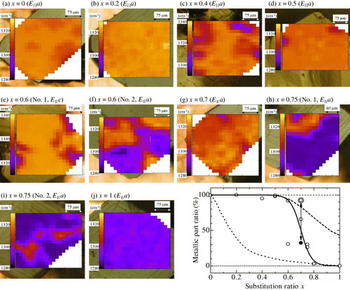
Relatively homogeneous metallic state is realized over the whole area of the samples with small substitution ratios of x=0 and 0.2. In contrast, the sample with x=1 exhibits a homogeneous insulating state. For intermediate levels of substitution, however, inhomogeneous features at a micrometer scale can be seen in the maps. Insulating domains appear on the dominant metallic background in samples with x=0.4 and 0.5. Such insulating domains tend to grow with increasing x. In the x=0.75 sample, the insulating region is dominant but the metallic domains remain.
The shape of the metallic and insulating domains is almost circular when these domains constitute a small portion of the image [Citation12]. On the other hand, the configuration of the metal and insulator regions in the intermediate x=0.6–0.75 samples is intricate, and there is no specific size or orientation with respect to the crystal axes. Also, none of the regions appear at a particular position such as a sample edge, step or scratch on the surface. To determine the time dependence of the phase separation, we performed SMIS two times at the same area of the same sample with a 20 h interval while maintaining the temperature at 4 K. The structure and position of each region were reproduced [Citation13]. Regarding the history of the temperature variation, however, the spatial variation and metal–insulator ratio of the phase separation depended on the thermal history and the cooling procedure such as the cooling speed [Citation13]. This indicates that the features of the phase separation strongly depend on how the cooling process of the sample passes through the first-order Mott transition.
The lower right panel of figure shows the dependence of the metallic part ratio on the substitution ratio x deduced from the histogram of the frequency distribution in each image in figure . Open circles indicate the results of the slowly cooled samples. Double and filled circles connected with an arrow are the results obtained using slow and rapid cooling for the same x=0.7 sample, respectively. The solid curve is a guide for the eyes. Dashed and dotted curves represent the superconducting volume fraction deduced from the bulk magnetization measurements using slow and rapid cooling, respectively [Citation41]. The almost complete metallization is observed up to x≃0.5 in both SMIS and magnetization experiments. The metallic part ratio decreases rapidly above x≃0.5, and almost complete insulating condition occurs at x=1. The decrease in the metallic part ratio in SMIS results is steeper than that in the magnetization results. The difference may originate from the following two reasons. One is the slightly higher cooling rate in the SMIS than in the magnetization experiments. Different cooling conditions may modify the bandwidth in the same way as the substitution of deuterated BEDT-TTF molecules. It may also appear in the metallic–insulating fraction ratio as a large sample dependence in the transition region of x=0.6–0.7. The other reason is the dissimilar measurement area in these two experiments. SMIS probes a surface layer of several μm thickness. Although it is representative of the bulk properties, SMIS may overestimate the insulating fraction near the surface. The effect of rapid cooling and the modification of the electronic state at the surface will be mentioned below.
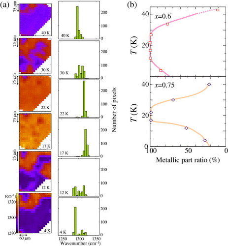
The reentrant transitions result in an S-shaped first-order Mott transition curve in the phase diagram of figure (a). Figure (a) presents the temperature variation of the two-dimensional contour maps for the peak frequency of the ν3(ag) mode and the frequency histograms for the x= 0.75 No. 1 (E||a) sample. The measurements were performed from low to high temperatures in sequence after slow cooling from room temperature to 4 K. The metal–insulator phase separation observed at 4 K changes to a metal-dominant state at approximately 20 K and subsequently to a bad metal state above 40 K. Near the boundary of the S-shaped Mott transition curve, the formation of the phase separation is observed at 12 and 30 K. The temperature dependence of the metallic part ratio deduced from the histograms of the contour maps is shown in figure (b) for the x=0.6 and 0.75 samples. The temperature dependence clearly demonstrates the reentrant nature of the S-shaped Mott transition curve. The observation of such a reentrant process of the phase separation suggests that it originates from the electron correlation.
Figure 12 (a) Temperature variation of the two-dimensional contour map of the peak frequency of the ν3(ag) mode (E||a-axis) and the frequency histogram for the x= 0.75 sample (from [Citation13]). (b) Temperature dependence of the metallic part ratio deduced from the histogram for κ-[(h-ET)1−x(d-ET)x]2Cu[N(CN)2]Br with x=0.6 and 0.75.
The observed phase separation is considered to originate from the bistability of the free energy between a Mott insulator and a correlated good metal and the subsequent superconductor. When the Mott transition takes place in the system with x≃ 0.5–0.8, the insulating domains appear in the correlated metal and superconducting matrix at lower temperature. The insulating part ratio increases with increasing x. The process of the phase separation is considered a nucleation and growth process rather than spinodal decomposition. This is because the pattern of the separation does not have the characteristics of spinodal decomposition, for example, the two separate regions tend to have a certain spacing and an interconnected random pattern.
Phase separation in the vicinity of the surface by rapid cooling
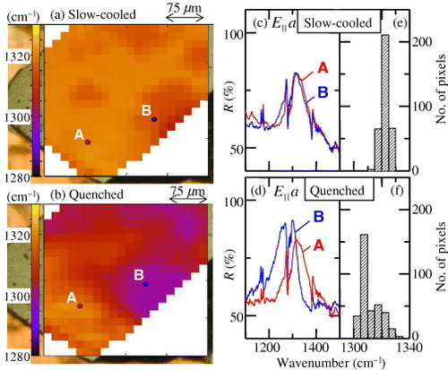
As mentioned before, the metal–insulator ratio in the phase separation is affected by the cooling condition in addition to the substitution ratio x. Under rapid cooling, SMIS of the superconducting sample κ-(h-ET)2Cu[N(CN)2]Br suggested that the insulating region was dominant as shown in figure (b), although the magnetization measurements indicated that the superconducting volume fraction was almost the same as that of the slowly cooled sample, that is, no insulating region was expected. This discrepancy may originate from the different parts of the sample scanned in the infrared and magnetization experiments. SMIS probes a micron-thick surface layer. If the insulating region is localized near the crystal surface then the SIMS may overestimate the insulating fraction. Why the insulating region might grow near the surface is unclear. It is speculated that more disorder is induced by fast cooling at the surface than in the bulk due to insufficient thermal flow. Such an inhomogeneous disorder may result in the present shell-type insulating state. Further study is needed to clarify the effect of the cooling rate on the inhomogeneity of the sample and its distribution. This is important for resolving the controversy regarding superconducting parameters such as the penetration depth [Citation14].
Figure 13 (a, b) Peak frequency maps of the ν3(ag) mode (E||a-axis) of κ-(h-ET)2Cu[N(CN)2]Br at 4 K using slow and rapid cooling conditions, respectively. (c, d) Reflectivity spectra at positions A and B in (a) and (b), respectively. (e, f) Frequency histograms of the ν3 peak frequency (from [Citation14]).
Summary
We present the imaging of the distribution of electronic states by spatial mapping of the infrared spectra (SMIS). Intense and collimated infrared light of the SPring-8 synchrotron is used to measure the local reflectivity spectra. Using SMIS, we obtained experimental evidence of the electronic phase separation in the organic Mott system κ-[(h-ET)1−x(d-ET)x]2Cu[N(CN)2]Br. SMIS combined with synchrotron radiation enabled us to demonstrate the macroscopic size of the domain structure of the insulating and metallic regions. The origin of the phase separation may be the strong electronic correlation at the first-order Mott transition. The observation of the macroscopic size of the domains of the phase separation, however, is in contrast to the recent findings of nanometer-scale electronic inhomogeneities in strongly correlated transition-metal oxides [Citation53, Citation54]. The reasons for the large size of the domains are not known yet. On the other hand, the present SMIS observations do not exclude the possibility of nanometer-scale inhomogeneities within our 10 μm beam. It is important to study the spatial inhomogeneity in correlated electron systems, including molecular materials, over a wide range of spatial resolutions and mapping areas from ∼nm2 to ∼mm2. In future, more complex systems can be studied. For example, the dynamical and nonequilibrium states subjected to high electromagnetic fields may produce novel critical phenomena [Citation55, Citation56]. Imaging measurements are important for understanding the nature of the electronic states in such complex phenomena. We hope that the present SMIS technique will be developed by improving the spatial resolution [Citation57] so that it becomes a more powerful tool for future studies.
Acknowledgments
The authors are grateful to A Suzuki, N Kobayashi (IMR, Tohoku University), H Kimura, Y Ikemoto, T Moriwaki, T Hirono and T Kawase (SPring-8/JASRI) for their collaboration. Synchrotron radiation experiments were performed at SPring-8 with the approval of JASRI. This work was partly supported by Grants-in-Aid for Scientific Research (No. 16076201, 17340099, 18654056 and 20340085) from JSPS and MEXT.
Notes
We have previously used SMIS as an abbreviation of scanning microregion infrared spectroscopy [Citation12, Citation13]. Instead of the former name, we call this method spatial mapping of infrared spectra measurement, which is abbreviated to SMIS measurement in this paper.
The phase diagram of κ-(BEDT-TTF)2X has been proposed in many reports [Citation6, Citation7, Citation23–25, Citation35–37]. Its general features are consistent, but the details, such as the transition temperatures, have not been fully settled yet.
We assign the vibrational features in accordance with [Citation42, Citation43] and references therein. Thus, the totally symmetric stretching mode is assigned as ν3(ag) in this paper. The lower symmetry of BEDT-TTF molecules has been predicted in κ-(BEDT-TTF)2Cu[N(CN)2]Br. Because of such reduced symmetry, reassignment of the totally symmetric
stretching mode as ν4 has been suggested [Citation44]. In this paper, we use ν3 for this mode, as before, to avoid any confusion.
The vibration at about 1380 cm−1 has been assigned as an ethylene bending mode [Citation42]. However, this mode did not change with deuteration and was not observed in the interplane (E||b-axis) spectrum [Citation45]. Furthermore, it was not observed in κ-(BEDT-TTF)2Cu(NCS)2 as shown in figure . The −CN mode may correspond to this vibration [Citation46]. This possibility has been pointed out in [Citation42] and also by Professor K Yakushi (private communication).
The peak position of the ν3(ag) mode is determined by simply taking the frequency at the maximum conductivity. When it was difficult to determine the peak frequency directly because of the overlapping terminal ethylene modes, we fitted a smooth curve for the ν3(ag) mode, which eliminated the sharp features of the ethylene modes.
Note that this flux value is calculated on the basis of the performance using the bare light source. The actual power at the sample position may decrease owing to the absorption in the windows, beam splitter and so on.
The frequency of the molecular vibration mode should be defined as the peak position of the optical conductivity. In most cases of the present SMIS measurements and their analyses, however, we simply used the peak positions of the reflectivity to make the contour map in order to reduce the calculations. Although there is a slight difference in the peak frequencies obtained from the optical conductivity and reflectivity, it does not affect the resultant contour maps.
References
- FainchteinRD'ArcangelisS TYangS SCowanD O 1992 Science 256 12 http://dx.doi.org/10.1126/science.256.5059.1012
- IshidaMTakeuchiOMoriTShigekawaH 2001 Phys. Rev. B 64 153405 http://dx.doi.org/10.1103/PhysRevB.64.153405
- YoneyamaNSasakiTNishizakiTTroyanovskiyA MKobayashiN 2006 J. Low Temp. Phys. 142 159 http://dx.doi.org/10.1007/BF02679486
- ColarussoPKidderL HLevinI WLewisE N 2000 Raman and Infrared Microspectroscopy (Encyclopedia of Spectroscopy and Spectrometry) J CLindon TGeorge JHolmes London Academic p 1945
- KatonJ E 1996 Micron 27 303 http://dx.doi.org/10.1016/S0968-4328(96)00045-5
- SasakiTItoIYoneyamaNKobayashiNHanasakiNTajimaHItoTIwasaY 2004 Phys. Rev. B 69 064508 http://dx.doi.org/10.1103/PhysRevB.69.064508
- KanodaK 1997 Hyperfine Interact. 104 235 http://dx.doi.org/10.1023/A:1012696314318
- KinoHFukuyamaH 1996 J. Phys. Soc. Japan 65 2158 http://dx.doi.org/10.1143/JPSJ.65.2158
- McKenzieR H 1997 Science 278 820 http://dx.doi.org/10.1126/science.278.5339.820
- RiceM J 1979 Solid State Commun. 31 93 http://dx.doi.org/10.1016/0038-1098(79)90175-3
- DresselMDrichkoN 2004 Chem. Rev. 104 5689 http://dx.doi.org/10.1021/cr030642f
- SasakiTYoneyamaNKobayashiNIkemotoYKimuraH 2004 Phys. Rev. Lett. 92 227001 http://dx.doi.org/10.1103/PhysRevLett.92.227001
- SasakiTYoneyamaNSuzukiAKobayashiNIkemotoYKimuraH 2005 J. Phys. Soc. Japan 74 2351 http://dx.doi.org/10.1143/JPSJ.74.2351
- YoneyamaNSasakiTKobayashiN 2005 Phys. Rev. B 72 214519 http://dx.doi.org/10.1103/PhysRevB.72.214519
- SasakiTYoneyamaNSuzukiAItoIKobayashiNIkemotoYKimuraHHanasakiNTajimaN 2006 J. Low. Temp. Phys. 142 377 http://dx.doi.org/10.1007/s10909-006-9121-z
- IkemotoYMoriwakiTHironoTKimuraSShinodaKMatsunamiMNagaiNNanbaNKobayashiKKimuraH 2004 Infrared Phys. Technol. 45 369 http://dx.doi.org/10.1016/j.infrared.2004.01.004
- ToyotaNLangMMüllerJ 2007 Low-Dimensional Molecular Metals Berlin Springer
- KomatsuTMatsukawaNInoueTSaitoG 1996 J. Phys. Soc. Japan 65 1340 http://dx.doi.org/10.1143/JPSJ.65.1340
- McKenzieR H 1998 Comments Condens. Matter. Phys. 18 309
- SasakiT,unpublished
- MiyagawaKKawamotoANakazawaYKanodaK 1995 Phys. Rev. Lett. 75 1174 http://dx.doi.org/10.1103/PhysRevLett.75.1174
- KagawaFMiyagawaKKanodaK 2005 Nature 436 534 http://dx.doi.org/10.1038/nature03806
- ItoHIshiguroTKubotaMSaitoG 1996 J. Phys. Soc. Japan 65 2987 http://dx.doi.org/10.1143/JPSJ.65.2987
- LefebvreSWzietekPBrownSBourbonnaisCJéromeDMézièreCFourmiguéMBatailP 2000 Phys. Rev. Lett. 85 5420 http://dx.doi.org/10.1103/PhysRevLett.85.5420
- SasakiTYoneyamaNMatsuyamaAKobayashiN 2002 Phys. Rev. B 65 060505 http://dx.doi.org/10.1103/PhysRevB.65.060505
- KagawaFItouTMiyagawaKKanodaK 2004 Phys. Rev. B 69 064511 http://dx.doi.org/10.1103/PhysRevB.69.064511
- SasakiTYoneyamaNKobayashiN 2008 Phys. Rev. B 77 054505 http://dx.doi.org/10.1103/PhysRevB.77.054505
- ShimizuYMiyagawaKKanodaKMaesatoMSaitoG 2003 Phys. Rev. Lett. 91 107001 http://dx.doi.org/10.1103/PhysRevLett.91.107001
- KurosakiYShimizuYMiyagawaKKanodaKSaitoG 2005 Phys. Rev. Lett. 95 177001 http://dx.doi.org/10.1103/PhysRevLett.95.177001
- YamashitaSNakazawaYOguniMOshimaYNojiriHShimizuYMiyagawaKKanodaK 2008 Nat. Phys. 4 459 http://dx.doi.org/10.1038/nphys942
- YamashitaMNakataNKasaharaYSasakiTYoneyamaNKobayashiNFujimotoSShibauchiTMatsudaY 2009 Nat. Phys. 5 44 http://dx.doi.org/10.1038/nphys1134
- MoritaHWatanabeSImadaM 2002 J. Phys. Soc. Japan 71 2109 http://dx.doi.org/10.1143/JPSJ.71.2109
- LeeS-SLeeP ASenthilT 2007 Phys. Rev. Lett. 98 067006 http://dx.doi.org/10.1103/PhysRevLett.98.067006
- SuXZuoFSchlueterJ AKellyM EWilliamsJ M 1999 Phys. Rev. B 57 14056 http://dx.doi.org/10.1103/PhysRevB.57.R14056
- MüllerJLangMSteglichFSchlueterJ AKiniA MSasakiT 2002 Phys. Rev. B 65 144521 http://dx.doi.org/10.1103/PhysRevB.65.144521
- FournierDPoirierMCastonguayMTruongK 2003 Phys. Rev. Lett. 90 127002 http://dx.doi.org/10.1103/PhysRevLett.90.127002
- LimelettePWzietekPFlorensSGeorgesACostiT APasquierCJéromeDMézièreCBatailP 2003 Phys. Rev. Lett. 91 016401 http://dx.doi.org/10.1103/PhysRevLett.91.016401
- YoneyamaNSasakiTNishizakiTKobayashiN 2004 J. Phys. Soc. Japan 73 184 http://dx.doi.org/10.1143/JPSJ.73.184
- YoneyamaNHigashiharaASasakiTNojimaTKobayashiN 2004 J. Phys. Soc. Japan 73 1290 http://dx.doi.org/10.1143/JPSJ.73.1290
- TaniguchiHKawamotoAKanodaK 1999 Phys. Rev. B 59 8424 http://dx.doi.org/10.1103/PhysRevB.59.8424
- YoneyamaNSasakiTKobayashiN 2004 J. Phys. Soc. Japan 73 1434 http://dx.doi.org/10.1143/JPSJ.73.1434
- EldridgeJ EKornelsonKWangH HWilliamsJ MCrouchA V SWatkinsD M 1991 Solid State Commun. 79 583 http://dx.doi.org/10.1016/0038-1098(91)90914-H
- MaksimukMYakushiKTaniguchiHKanodaKKawamotoA 2001 J. Phys. Soc. Japan 70 3728 http://dx.doi.org/10.1143/JPSJ.70.3728
- WesolowskiRHaraldsenJ TCaoJMusfeldtJ LOlejniczakIChoiJWangY JSchlueterJ A 2005 Phys. Rev. B 71 214514 http://dx.doi.org/10.1103/PhysRevB.71.214514
- McGuireJ JRoomTProninATimuskTSchlueterJ AKellyM EKiniA M 2001 Phys. Rev. B 64 094503 http://dx.doi.org/10.1103/PhysRevB.64.094503
- NagASchmidtP JSchnickW 2006 Chem. Mater. 18 5738 http://dx.doi.org/10.1021/cm0607029
- MiyagawaKKawamotoAKanodaK 2002 Phys. Rev. Lett. 89 017003 http://dx.doi.org/10.1103/PhysRevLett.89.017003
- TaniguchiHKanodaHKawamotoA 2003 Phys. Rev. B 67 014510 http://dx.doi.org/10.1103/PhysRevB.67.014510
- FaltermeierDBarzJDummMDresselMDrichkoNPetrovBSemkinVVlasovaRMeźièreCBatailP 2007 Phys. Rev. B 76 165113 http://dx.doi.org/10.1103/PhysRevB.76.165113
- MoriwakiTIkemotoY 2008 Infrared Phys. Technol. 51 400 http://dx.doi.org/10.1016/j.infrared.2007.12.031
- SatoM 2007 Bull. Natl Res. Inst. Cultural Properties, Nara 2007 32
- NishiTKimuraSTakahashiTItoTImH JKwonY SMiyagawaKTaniguchiHKawamotoAKanodaK 2005 Solid State Commun. 134 189 http://dx.doi.org/10.1016/j.ssc.2005.01.026
- HanaguriTLuplenCKohsakaYLeeD-HAzumaMTakanoMTakagiHDavisJ C 2004 Nature 430 1001 http://dx.doi.org/10.1038/nature02861
- FäthMFresemSMenovskyA ATomiokaYAartsJMydoshJ A 1999 Science 285 1540 http://dx.doi.org/10.1126/science.285.5433.1540
- KumaiROkimotoYTokuraY 1999 Science 284 1645 http://dx.doi.org/10.1126/science.284.5420.1645
- SawanoFTerasakiIMoriHMoriTWatanabeMIkedaNNogamiYNodaY 2005 Nature 437 522 http://dx.doi.org/10.1038/nature04087
- IkemotoYMoriwakiTOkamuraHSasakiTYoneyamaNTaguchiAInouyeYKawataSKinoshitaT 2008 Infrared Phys. Technol. 51 417 http://dx.doi.org/10.1016/j.infrared.2007.12.016