Abstract
Spatially and spectrally resolved low-energy cathodoluminescence (CL) microscopy was applied to the characterization of nanostructures. CL has the advantage of revealing not only the presence of luminescence centers but also their spatial distribution. The use of electrons as an excitation source allows a direct comparison with other electron-beam techniques. Thus, CL is a powerful method to correlate luminescence with the sample structure and to clarify the origin of the luminescence. However, caution is needed in the quantitative analysis of CL measurements. In this review, the advantages of cathodoluminescence for qualitative analysis and disadvantages for quantitative analysis are presented on the example of nanostructures.
Introduction
Optical characterization of nanostructures is usually performed by statistically averaging their ensemble. However, this approach is imprecise and sometimes misleading due to the possible coexistence of materials with different optical properties. With the development of low-dimensional optoelectronic materials, the investigation of local variations of luminescence is gaining importance [Citation1, Citation2]. The low-energy cathodoluminescence (CL) technique has decisive advantages for this purpose. It allows characterization of individual nanostructures that can be used to evaluate materials for industrial applications, such as field emission displays. With CL, one can also map the luminescence distribution both laterally and along the sample depth that can provide precious information on the growth mechanisms. Finally, the combination of CL with other electron beam (e-beam) techniques allows to determine the origin of the luminescence.
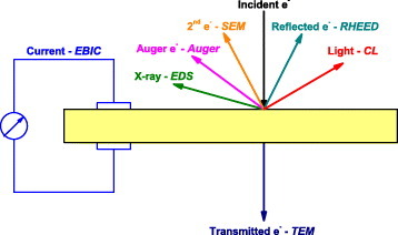
CL is the emission of light from a material under e-beam irradiation [Citation3, Citation4]. Compared with light, electron excitation is rather strong. The incident electrons generate a high density of electron–hole (e–h) pairs due to inelastic scattering—it is commonly accepted that an incident electron of energy E can generate ∼E/3Eg pairs [Citation3, Citation4]. Those e–h pairs can recombine and emit photons. The energy of these photons depends on the energy difference between the electrons and holes, which is related to the bandgap Eg or to the energy levels of the impurities and defects. Consequently, CL can reveal most of the luminescence processes in the materials. Especially, the electron beam can excite high energy levels allowing to characterize deep ultraviolet (UV) emission from wide-bandgap materials, such as BN, which is very difficult to study with light-induced luminescence. Development of the electron microscopes improved control of the size and the position of the electron beam, allowing to acquire luminescence from nanoscale regions. By changing the energy of the incident electrons, it is possible to excite the material at different depths: the surface can be excited by low energy and deeper regions by higher energy electrons [Citation5]. In this way, CL allows a lateral and depth resolved analysis of the distribution of luminescence centers present in the material. It should be noted that, although the CL generation volume is mainly related to the electron penetration range, it is also affected by the minority carrier diffusion, because light is generated not where the e–h pairs are generated, but where they recombine [Citation6]. However, in semiconductor nanostructures, such diffusion is limited by the quantum confinement [Citation7] and surface effects [Citation8]. Finally, as illustrated in figure , the interaction of incident electrons with the material can generate various signals, which provide different information on the materials. Beside the optical properties from CL, structural information can be obtained from reflected (reflection high-energy electron diffraction, RHEED) and transmitted electrons (transmission electron microscopy, TEM), surface morphology from secondary electrons (scanning electron microscopy, SEM), chemical structure from Auger electrons (Auger electron spectroscopy) and x-rays (energy-dispersive x-ray spectroscopy, EDS) and electrical properties from the current induced due to the separation of generated e–h pairs (electron-beam induced current, EBIC). The combination of these techniques with CL results in a better understanding of the origin of the luminescence.
Figure 1 Schematic illustration of the signals generated by the electron irradiation of a non-metallic solid.
In summary, the advantages of CL for the characterization of the nanostructures are:
Local excitation, allowing to map the lateral and depth distribution of the luminescence centers.
Combination with other electron-based techniques, allowing to correlate optical, structural, chemical and electrical properties.
Strong excitation, allowing to excite emission from deep UV to infrared (IR) spectral range.
Experimental details
Cathodoluminescence system
CL measurements were performed with an SEM-based setup, which consists of a light collector, detection system and computer controller, as illustrated in figure . The electron source is a Schottky-type field emission electron gun (Omicron, Germany), allowing a beam diameter of the order of tens of nanometers. The electron energy can be varied from 1.5 to 25 kV. To reduce the surface contamination, we adopted an ultra-high vacuum system (less than 2×10⁻¹⁰ mbar).
Figure 2 Photographs of the UHV-SEM CL system and the ellipsoidal mirror (a) and the block diagram of the CL system (b).
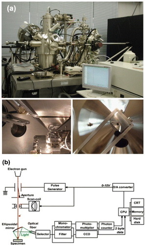
The light-collection system consists of an ellipsoidal mirror of low magnification and an optical fiber. The ellipsoidal mirror is designed to realize both high and uniform collection efficiency. One focal point of the ellipsoid is set at the specimen position and another at the entrance edge of the optical fiber. Thus, the CL emission is focused on the entrance edge of the optical fiber and guided into a triple-grating monochromator (Jobin-Yvon Triax320). In spectral measurements, the dispersed light is detected by a charge-coupled device with 2048 channels (CCD, Jobin-Yvon Spectrum One). Parallel detection of the spectrum with the CCD significantly reduces the acquisition time compared with the serial detection using a photomultiplier. One- or two-dimensional spectral mapping is also possible with this system. For imaging, monochromatic light is guided to the photomultiplier (Hamamatsu R943-02 or R3310-02). A photon counting system is adopted to record light emitted from each pixel point. The spectral resolution is determined by the grating and the slit width and is typically 0.2 nm.
Samples
The studied samples were rare-earth doped oxynitride phosphors (Ca and Yb codoped α-SiAlON and Eu-doped AlN) synthesized by gas-pressure sintering [Citation9–14], Zn2SiO4 nanotubes obtained by reacting ZnO nanowires with SiO2 [Citation15], ZnGa2O4 nanowires grown by chemical vapor deposition (CVD) [Citation16] and different types of ZnO materials. The latter included nanotubes (grown by metal organic chemical vapor deposition, MOCVD) [Citation17, Citation18], nanoparticles (vapor method) [Citation19], nanoflowers (hydrothermal method) [Citation20], tetrapods composed of nanorods (catalyst-free vapor-solid growth) [Citation21], polycrystals [Citation22] and single crystals (hydrothermal synthesis) [Citation23].
Advantages of CL
Local excitation
Spatial distribution
The main advantage of CL microscopy is local excitation, which makes it especially suitable for optical characterization of nanostructures. Precise control of the size and position of the e-beam in the electron microscope allows to acquire a CL spectrum from a nanoscale region. Moreover, by scanning the material, it is possible to obtain high-resolution CL images of the luminescence centers [Citation15, Citation21, Citation24–29]. Such information is important for nanomaterials as it can provide information about the growth mechanisms.
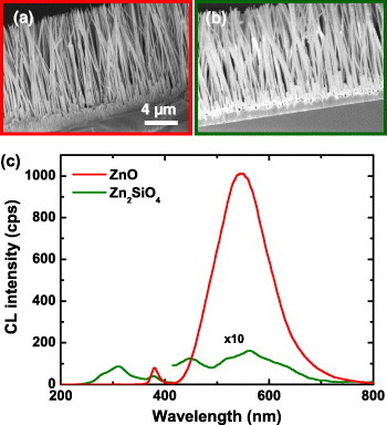
We have investigated the luminescence properties of Zn2SiO4 nanotubes on Si substrate. The tubes were synthesized from ZnO nanowires reacting with SiO2 [Citation15]. Figure shows cross-sectional SEM images of ZnO nanowires (a) and Zn2SiO4 nanotubes (b) and their averaged CL spectra (c) at 5 kV and 1.0 nA. The SEM images reveal that the Zn2SiO4 nanotubes are thicker than the ZnO nanowires due to the formation of a SiO2 coating [Citation15]. Both the ZnO nanowires and Zn2SiO4 nanotubes lie on a buffer layer. The CL spectrum of the ZnO nanowires consists of excitonic emission at 380 nm and a broad band at 550 nm related to defects and/or impurities in ZnO [Citation30, Citation31]. The CL spectrum of the Zn2SiO4 nanotubes, in addition to these two peaks at 380 and 550 nm, has two new bands at 310 and 440 nm. The 310 nm emission is attributed to defects in Zn2SiO4 [Citation32] and the 440 nm peak to defects in SiO2 [Citation33].
Figure 3 Cross-sectional SEM images of ZnO nanowires (a) and Zn2SiO4 nanotubes (b), and their CL spectra (c) at 5 kV and 1.0 nA.
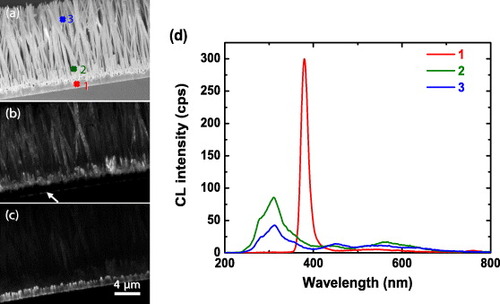
The presence of the peak at 380 nm (excitonic emission of ZnO) from the Zn2SiO4 nanotubes sample indicates that the ZnO nanowires are only partly reacted with SiO2 and some ZnO still remains. To test this hypothesis we mapped the CL distribution of the 310 and 380 nm emission. Figure shows the SEM images of Zn2SiO4 nanotubes (a) and the corresponding CL images recorded at 310 nm (b) and 380 nm (c) with the e-beam voltage of 5 kV and 1.0 nA current. The 310 nm emission (defects of Zn2SiO4) is produced by the Zn2SiO4 nanotubes, whereas the 380 nm light (excitonic emission of ZnO) originates from the buffer layer. Moreover, the interface between the Si substrate and the buffer layer (indicated by the white arrow) has a clear 310 nm emission, suggesting that this interface consists of Zn2SiO4. To clarify this result, CL spectra were taken from the buffet layer and the nanotubes. The CL spectrum from the buffer (point 1) consists of a sharp and strong peak at 380 nm, and a small peak at 550 nm. On the nanotubes (points 2 and 3), the 380 nm peak disappears, while the 310 nm emission emerges. These results demonstrate that the original ZnO nanowires have reacted with SiO2 to form Zn2SiO4 nanotubes, but the buffer layer is still ZnO.
Figure 4 SEM images of Zn2SiO4 nanotubes (a) and the corresponding CL images of 310 nm (b) and 380 nm (c) emission generated at 5 kV and 1.0 nA. Panel (d) presents CL spectra taken at 5 kV and 1.0 nA from the buffer layer and the nanotubes at locations indicated in (a).
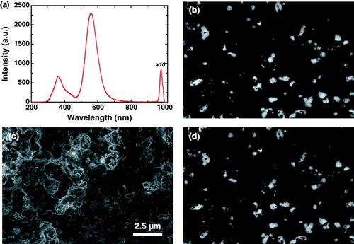
The 310 nm emission (defects of Zn2SiO4) is not uniformly distributed along the Zn2SiO4 nanotubes (figure (b)). To reveal this inhomogeneity, a low packing density sample was made by removing Zn2SiO4 nanotubes from the Si substrate and depositing them on a TEM grid. Figure shows the CL image of 310 nm emission from a region where Zn2SiO4 nanotubes have low density. CL from some tubes is rather uniform, but it shows bright dots along other tubes. Possibly, the uniform nanotubes consist of Zn2SiO4 nanotubes coated with SiO2, and the non-uniform ones are Zn2SiO4 nanoparticles encapsulated in SiO2 nanotubes. The ZnO nanowires may react with SiO2 by different mechanisms, such as Rayleigh instability and the Kirkendall solid-state reaction, which may result in the different tube structures [Citation15].
Figure 5 CL image of 310 nm emission from a low packing density Zn2SiO4 nanotubes, which were removed from the Si substrate and deposited on a TEM grid.
Depth distribution
Not only the lateral but also the depth distribution of luminescence is important for the characterization of nanostructures. For instance, some nanostructures may be covered with oxide or other layers. There may also be some concentration gradient of defects, such as vacancies or impurities between the surface and the core of the nanostructures. By changing the electron energy, it is possible to vary the penetration depth of the incident electrons and excite the luminescence centers at different depth [Citation34–37].
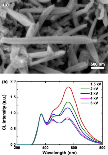
We have investigated the depth distribution of luminescence from ZnGa2O4 nanorods [Citation16]. Figure shows the SEM image of the nanorods (a) and the CL spectra (b) taken by varying the incident electron energy from 1.5 to 5 kV. For comparison, the CL spectra were normalized by the intensity at 360 nm. The luminescence consists of three peaks at 360, 450 and 550 nm, which are attributed to different defects in ZnGa2O4 [Citation38–40]. At 1.5 kV, the 450 and 550 nm bands are stronger than that at 360 nm. When the electron energy is raised to 5 kV, the 360 nm peak increases more than those of 450 and 550 nm and becomes dominant. The results suggest inhomogeneous defect distribution in the core and the surface regions.
Figure 6 SEM image of ZnGa2O4 nanorods (a) and CL spectra (b) taken by varying the incident electron energy from 1.5 to 5 kV.
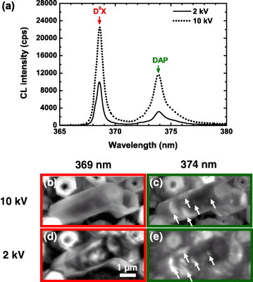
By comparing the CL images taken at different accelerating voltage, it is possible to deduce the lateral and depth distribution of the luminescence centers. We have analyzed the luminescence from shallow levels of ZnO nanotubes grown on sapphire [Citation18]. Figure (a) shows the CL spectra of a tilted ZnO nanotube recorded at 10 kV/0.8 nA and 2 kV/0.2 nA at temperature of 10 K. The excitation depth of the 2 kV electrons (penetration depth ∼50 nm) [Citation5] allows revealing the thin walls of the tilted tubes, which have a thickness of about 150 nm. Electrons with the energy of 10 kV stop at the depth of ∼740 nm [Citation5] and thus penetrate through the nanotubes; their CL signals are averaged over the nanotube thickness. The spectra consist of two peaks at 369 and 374 nm which are attributed to neutral donor excitonic emission (D0X) and donor–acceptor pairs (DAP) transitions, respectively [Citation41, Citation42]. We can assume that the intensities of the 369 nm (D0X) and 374 nm (DAP) signals reflect the concentrations of donors and acceptors, respectively, at least for small defect concentrations. The CL images were taken for the 369 nm (b, d) and 374 nm (c, e) emissions in a tilted ZnO nanotube at 10 and 2 kV, respectively. For the D0X (369 nm) luminescence, the 10 kV and 2 kV CL images are obviously different. Whereas the 10 kV distribution is relatively uniform, the 2 kV image clearly shows some patches along the nanotubes. On the contrary, the 10 kV and 2 kV CL images are rather similar for the DAP (374 nm) luminescence. The DAP luminescence is localized on some patches along the nanotubes, as indicated by the white arrows. The thus revealed inhomogeneous distribution of the donors and acceptors can be related to the unstable growth conditions and contaminations from the substrate and growth chamber.
Figure 7 CL spectra of a tilted ZnO nanotube recorded at 10 kV/0.8 nA and 2 keV/0.2 nA at 10 K (a). CL images of 369 nm (b, d) and 374 nm (c, e) emissions for a tilted ZnO nanotube at 10 and 2 kV, respectively.
Comparison with other e-beam techniques
Although luminescence and its distribution can be characterized with CL, this technique does not always supply enough information about the nature of the luminescence centers. In such cases, it is necessary to combine it with other techniques. Since the incident electrons can generate other signals beside CL, it is possible to correlate the light emission with electrical, chemical and structural properties. The correlation of CL with high-resolution TEM (HRTEM) and EBIC has been used to characterize defects, such as dislocations or stacking faults [Citation43–47]. As for the variation of concentration/composition, the combination of CL with TEM, EDS or Auger spectroscopy can result in a better understanding of the origin of the luminescence [Citation48, Citation49]. Here, we illustrate this aspect by the analysis of europium doping of AlN using the combination of CL and EDS [Citation14].
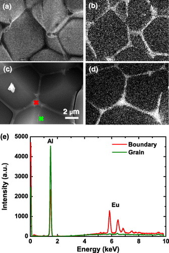
Figure shows the normalized CL spectra of undoped AlN and AlN:Eu (AlN doped with 0.2% Eu). The CL spectrum of undoped AlN shows a peak at 360 nm which is attributed to defects [Citation50]. The CL spectrum of AlN:Eu consists of a strong peak at 360 nm and a weak band at 550 nm. Because the 550 nm peak appears with Eu doping, it would be reasonable to assign it to Eu2+ in AlN, as it was done by Hara et al [Citation51]. However, this is not correct. Figures (a) and (b) show the CL images of 360 and 550 nm emissions in AlN:Eu, respectively. Whereas the 360 nm emission (defects in AlN) is almost uniform, the 550 nm band is restricted to the grain boundaries and therefore is hardly due to Eu2+ in AlN. SEM–EDS measurements were performed to confirm this result and clarify the origin of this emission. Figures (c) and (d) show the SEM image and the corresponding EDS image of the Eu distribution. Similar to the 550 nm CL signal, europium is concentrated at the grain boundaries. EDS spectra were taken from the bulk of a grain and its surface (positions indicated in figure (c)), as shown in figure (e). No europium is detected in the bulk, whereas the grain boundary contains much Eu and less Al than the bulk AlN. Europium has low solubility in AlN and might form secondary phases at the surface, which is responsible for the 550 nm emission. The existence of such secondary phase was also confirmed by XRD [Citation14]. Thus, the attribution of the 550 nm emission to Eu2+ in AlN, based only on emission spectrum, is incorrect. This example illustrates the difficulties in deducing the origin of luminescence peaks [Citation52].
Figure 8 Normalized CL spectra for undoped AlN and AlN doped with 0.2% Eu.
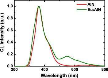
Figure 9 CL images of 360 nm (a) and 550 nm (b) emission of AlN:Eu. SEM image (c) and EDS image (d) of Eu distribution. Panel (e) shows EDS spectra taken from the grain and the grain boundary, as indicated in (c).
Strong excitation
The energy of electrons used in CL setup is sufficient to excite almost any luminescence center in the studied material, with the emission spectrum ranging from the ultraviolet to the infrared region [Citation53]. In contrast, the excitation capabilities of photoluminescence (PL) are limited by the incident photon energy [Citation54–56]. As a result, it is easier to study deep UV emission with CL than PL [Citation57–60]. In addition, whereas one incident photon can generate not more than one e–h pair, one incident electron of energy E produces ∼E/3Eg pairs, where Eg is the band gap of the material [Citation3, Citation4], i.e. orders of magnitude more than one photon.
We have investigated by CL the optical properties of Ca- and Yb-doped α-SiAlON with a composition of Ca0.095Yb0.005Si6.75Al5.25O1.75N14.25 [Citation10, Citation11]. Figure (a) shows the CL spectrum of Ca- and Yb-doped α-SiAlON. The CL spectrum shows a broad band in the green region peaking at 557 nm, which is related to the 4f135d1→ 4f14 transition of Yb2+ [Citation9], but also a broad peak in the UV region (360 nm) and a sharp peak in the IR region (980 nm). The 360 nm emission is attributed to an AlN secondary phase [Citation50] and the 980 nm emission to an inner 4f–4f transition of Yb3+ [Citation61]. To clarify the relation between these emissions, CL images were taken at 360 (b), 557 (c) and 980 nm (d). The Yb2+ emission (557 nm) is fairly uniformly distributed in the particles except for the brighter particle edges. The luminescence from AlN secondary phase (360 nm) is observed in several large bright patches. This distribution of the AlN phase was confirmed by the electron probe microanalysis [Citation11]. The distribution of Yb3+ emission (980 nm) is similar to that of the secondary phase (360 nm), which means that Yb3+ and the AlN secondary phase are related. Therefore, CL reveals that Yb is incorporated in both the α-SiAlON and the AlN phases, but with different valence due to the charge balance.
Figure 10 CL spectrum (5 kV) of Ca- and Yb-doped α-SiAlON (a). CL images of 360 nm (b), 557 nm (c) and 980 nm (d) emission.
Caution on the quantitative analysis of CL results
As shown in the previous section, with CL it is possible to detect luminescence centers and map their spatial distribution that makes CL a useful qualitative technique. Knowing the e–h pair recombination volume, one may also expect to use CL quantitatively [Citation62]. However, caution is required here because the CL intensity depends on the electron beam parameters, internal light absorption, sample damage by the beam and other factors.
Measurement conditions
CL results depend not only on the excitation conditions, namely beam current and electron energy, but also on the specimen preparation. Indeed, because CL measurements are rather local, a small variation of these parameters may significantly change the CL intensity.
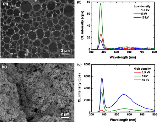
As an example, we have investigated two samples of the same material having dissimilar concentration of nanoparticles [Citation19]. Different weights of commercial ZnO nanoparticles were dispersed in 5 ml of ethanol to prepare a ‘low-density’ sample with small segregation and ‘high-density’ sample with significant agglomeration of particles. Figure shows the SEM images and the CL spectra for low (a, b) and high density (c, d) specimens taken at 1.5, 5 and 15 kV at 1 nA. For the low-density sample, the CL spectrum consists of an excitonic peak at 375 nm; its intensity is the weakest for 15 kV and strongest for the 5 kV excitation. No clear peaks are observed in the visible spectral range. On the contrary, for the high-density sample the UV intensity increases with the electron energy, and the UV peak shifts to the longer wavelength. A clear visible-light peak appears and its intensity increases with the increasing electron energy. The observed change of the UV peak can be related to the generation volume of the e–h pairs. For the low-density sample, the penetration depth of the 5 kV e-beam is comparable to the size of the segregated particles. As the electron energy is increased, the penetration depth exceeds the size of the agglomerated particles and most of the incident electrons pass through the nanoparticles without generating e–h pairs. Thus, the number of generated carriers per nanoparticle and the CL intensity decrease in the low-density sample for the 15 kV excitation. The opposite intensity behavior is observed for the high-density sample because of the larger size of its aggregated particle clusters, and thus a large volume is excited with 15 kV than 5 kV electrons. The saturation of the UV emission and the supralinear increase of visible emission for high-energy electrons in the high-density sample can be explained by the reabsorption of the UV light from the deeper region by the emission centers near the surface [Citation36, Citation37, Citation63]. The reabsorbed UV light generates secondary electron–hole pairs and contributes to a new recombination process, which may result in the reemission of UV light or generation of visible light. Thus, a part of UV emission is converted into visible light. The excitonic emission should suffer stronger absorption than the shallow-level emission. This explains the redshift of the UV peak position. Thus, due to the variation of the generation volume and secondary excitation, different CL results can be obtained from the very same nanoparticles dispersed to different densities.
Figure 11 SEM images and CL spectra for low (a, b) and high density (c, d) specimens taken at 1.5, 5 and 15 kV and 1 nA.
Variation of the CL intensity during the measurements
Another difficulty in CL observations is the change of the luminescence during the measurements. Relatively high energy of the electron beam increases the chance of sample damage during the CL measurements as compared to PL. This damage can occur via different mechanisms, such as adsorption/desorption or charging at the surfaces, creation or activation of defects, etc [Citation64–71]. Such e-beam induced effects reduce the reliability of quantitative CL measurements.
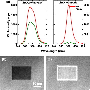
We have observed a significant degradation of the CL intensity in ZnO [Citation21, Citation22, Citation70, Citation71]. Figure (a) shows the CL spectra of a bulk ZnO polycrystal and nanorod-structured ZnO tetrapods, after 20 and 3600 s of irradiation at 5 kV. The UV intensity decreases from 5600 to 3500 counts per second (cps) for ZnO polycrystal and from 2000 to 100 cps for the ZnO tetrapods. This result reveals more serious degradation in nanostructures, which have the higher surface/volume ratio. We have also tested CL stability in ZnO single crystals with (000–1)/O-terminated surface and (0001)/Zn-terminated surfaces [Citation23]. Figures (b) and (c) show the respective CL images of the O- and Zn-faces irradiated for 3600 s. The luminescence is weaker in the irradiated than in the unirradiated area for the O-face, but it is stronger for the Zn-face. This experiment suggests that the surface plays an important role in the variation of the intensity during CL measurements [Citation71].
Figure 12 CL spectra of ZnO polycrystal and ZnO tetrapods after 20 and 3600 s of irradiation at 5 kV (a). CL images of an area irradiated at 5 kV for 1 h for O- (a) and Zn-terminated (b) faces of a ZnO single crystal.
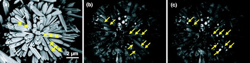
Although these intensity variations complicate the quantitative analysis of CL results, they can be used to investigate the lifetime of optoelectronic devices. Additionally, the e-beam induced effects can be intentionally used to locally alter the luminescence that can be applied to high-density optical data storage or high-resolution UV-emission displays. For such demonstration, we have irradiated some portions of ZnO nanoflowers for 20 s at 5 kV. Figure shows the SEM (a) and CL images of the UV emissions before (b) and after irradiation (c) revealing the brightening of the UV emission from the parts marked by arrows.
Figure 13 SEM (a) and CL images of the UV emissions before (b) and after (c) 20 s irradiation at 5 kV.
Conclusion
We have demonstrated the advantages of CL for luminescence characterization. By revealing the luminescence centers in the material and their spatial distribution, CL can clarify the origin of emission peaks and the growth mechanism. However, the measurement conditions and the e-beam induced degradation must be taken into consideration for quantitative analysis of CL results. When using CL with such caution, it becomes an invaluable technique for the characterization of optoelectronic materials.
Acknowledgments
The authors are grateful to Professor B P Zhang (Xiamen University) for provision of ZnO nanotubes, Dr B D Liu (MANA, NIMS) for ZnGa2O4 nanorods, Dr C Li (MANA, NIMS) for Zn2SiO4 nanotubes, Dr U K Gautam (MANA, NIMS) for ZnO nanoflowers, Dr N Hirosaki and Dr R-J Xie (NIMS) for rare-earth doped oxynitrides, and Dr L Lazzarini and Professor G Salviati (IMEM-CNR Institute) for ZnO tetrapods. The authors also wish to thank Mr Ray Phillips of Julius Kruttschnitt Mineral Research Centre, University of Queensland, Australia, for a discussion and improvement of the manuscript.
References
- GustafssomAPistolM EMonteliusLSamuelsonL 1998 J. Appl. Phys. 84 1715 http://dx.doi.org/10.1063/1.368613
- GustafssonAKaponE 1998 Scanning Microsc. 12 285
- YacobiB GHoltD B 1990 Cathodoluminescence Microscopy of Inorganic Solids New York Plenum
- YacobiB GHoltD B 1985 J. Appl. Phys. 59 R1 http://dx.doi.org/10.1063/1.336491
- KanayaKOkayamaS 1972 J. Phys D: Appl. Phys. 5 43 http://dx.doi.org/10.1088/0022-3727/5/1/308
- TothMPhilipsM R 1998 Scanning 20 425 http://dx.doi.org/10.1002/sca.1998.4950200601
- FonoberovV ABalandinA A 2004 Appl. Phys. Lett. 85 5971 http://dx.doi.org/10.1063/1.1835992
- SoudiADhakalPGuY 2010 Appl. Phys. Lett. 96 253115 http://dx.doi.org/10.1063/1.3456390
- XieR-JHirosakiNMitomoMUhedaKSuehiroTXuXYamamotoYSekiguchiT 2005 J. Phys. Chem. B 109 9490 http://dx.doi.org/10.1021/jp050580s
- DierreBYuanX LHirosakiNXieR-JSekiguchiT 2008 Mater. Sci. Eng. B 146 80 http://dx.doi.org/10.1016/j.mseb.2007.07.047
- DierreBYuanX LHirosakiNKimuraTXieR-JSekiguchiT 2008 J. Mater. Res. 23 1701 http://dx.doi.org/10.1557/jmr.2008.0208
- HirosakiNXieR-JInoueKSekiguchiTDierreBTamuraK 2007 Appl. Phys. Lett. 91 061101 http://dx.doi.org/10.1063/1.2767182
- InoueKHirosakiNXieR-JTakedaT 2009 J. Phys. Chem. C 113 9392 http://dx.doi.org/10.1021/jp901327j
- DierreBYuanX LInoueKHirosakiNXieR-JSekiguchiT 2009 J. Am. Ceram. Soc. 92 1272 http://dx.doi.org/10.1111/j.1551-2916.2009.03048.x
- LiCBandoYDierreBSekiguchiTHuangYLinJGolbergD 2010 Nanoscale Res. Lett. 5 773 http://dx.doi.org/10.1007/s11671-010-9556-7
- LiuB DBandoYDierreBSekiguchiTTangC CMitomeMWuA MJiangXGolbergD 2009 Nanotechnology 20 365705 http://dx.doi.org/10.1088/0957-4484/20/36/365705
- YuanX LZhangB PNiitsumaJSekiguchiT 2006 Mater. Sci. Semicond. Proc. 9 146 http://dx.doi.org/10.1016/j.mssp.2006.01.037
- YuanX LDierreBWangJ BZhangB PSekiguchiT 2007 J. Nanosci. Nanotechnol. 7 3323 http://dx.doi.org/10.1166/jnn.2007.661
- DierreBYuanX LOhashiNSekiguchiT 2008 J. Appl. Phys. 103 083551 http://dx.doi.org/10.1063/1.2904858
- GautamU K et al 2010 Proc. Natl. Acad. Sci. USA doi:10.1073pnas.1008240107
- LazzariniLSalviatiGFabbriFZhaM ZCalestaniDZappettiniASekiguchiTDierreB 2009 ACS Nano 3 3158 http://dx.doi.org/10.1021/nn900558q
- DierreBYuanX LYaoY ZYokoyamaMSekiguchiT 2008 J. Mater. Sci: Mater. Electron. 19 S307 http://dx.doi.org/10.1007/s10854-008-9603-7
- DierreBYuanX LSekiguchiT 2008 J. Appl. Phys. 104 043528 http://dx.doi.org/10.1063/1.2973190
- HidalgoPPiquerasJSochinskiiN VAbellánMSaucedoEDiéguezE 2008 J. Mater. Sci. 43 5605 http://dx.doi.org/10.1007/s10853-008-2815-7
- WeiT BDuanR FWangJ XLiJ MHuoZ QZengY P 2008 Microelectron. J. 39 1556 http://dx.doi.org/10.1016/j.mejo.2008.02.024
- YanJFangX SZhangLBandoYGautamU KDierreBSekiguchiTGolbergD 2008 Nano Lett. 8 2794 http://dx.doi.org/10.1021/nl801353c
- CallejaESánchez-GarciaM ASánchezF JCalleFNaranjoF BMuñozEJahnUPloogK 2000 Phys. Rev. B 62 16826 http://dx.doi.org/10.1103/PhysRevB.62.16826
- ZollfrankCRamboC RBatentschukMGreilP 2007 J. Mater. Sci. 42 6325 http://dx.doi.org/10.1007/s10853-006-1253-7
- JungM NHaS YParkS HYangMKimH SLeeW HYaoTChangJ H 2006 Physica E 31 187 http://dx.doi.org/10.1016/j.physe.2005.12.114
- SekiguchiTMiyashitaSObaraKShishidoTSakagamiN 2000 J. Cryst. Growth 214/215 72 http://dx.doi.org/10.1016/S0022-0248(00)00065-8
- StrassburgM et al 2004 Phys. Status Solidi b 241 607 http://dx.doi.org/10.1002/pssb.200304187
- FengXYuanX LSekiguchiTLinW ZKangJ Y 2005 J. Phys. Chem. B 100 15786 http://dx.doi.org/10.1021/jp0514980
- YuD PHangQ LDingYZhangH ZBaiZ GWangJ JZouY HQianWXiongG CFengS Q 1998 Appl. Phys. Lett. 73 3076 http://dx.doi.org/10.1063/1.122677
- GautamU KPanchakarlaL SDierreBFangX SBandoYSekiguchiTGovindarajAGolbergDRaoC N R 2009 Adv. Funct. Mater. 19 131 http://dx.doi.org/10.1002/adfm.200801259
- BrillsonL J et al 2002 Appl. Surf. Sci. 190 498 http://dx.doi.org/10.1016/S0169-4332(01)00925-4
- BrillsonL JMosbackerH LDouttD LDongYFangZ QLookD CCantwellGZhangJSongJ J 2009 Superlattice Microstruct. 45 206 http://dx.doi.org/10.1016/j.spmi.2008.11.008
- OngH CLiA S KDuG T 2001 Appl. Phys. Lett. 78 2667 http://dx.doi.org/10.1063/1.1368187
- KimJ S et al 2003 Appl. Phys. Lett. 82 2029 http://dx.doi.org/10.1063/1.1564632
- HsiehI JChuK TYuC FFengM S 1994 J. Appl. Phys. 76 3735 http://dx.doi.org/10.1063/1.358500
- HuJ QBandoYLiuZ W 2003 Adv. Mater. 15 1000 http://dx.doi.org/10.1002/adma.200304825
- ZhangB PManhL HWakatsukiKOhnishiTLippmaaMUsamiNKawasakiMSegawaY 2003 Japan. J. Appl. Phys. 42 2291 http://dx.doi.org/10.1143/JJAP.42.2291
- ZhangB PBinhN TSegawaYWakatsukiKUsamiN 2003 Appl. Phys. Lett. 83 1635 http://dx.doi.org/10.1063/1.1605803
- SugaharaTSataHHaoM SNaoiYKuraiSTottoriSYamashitaKNishinoKRomanoL TSakaiS 1998 Japan. J. Appl. Phys. 37 L398 http://dx.doi.org/10.1143/JJAP.37.L398
- ThonkeKSchirraMSchneiderRReiserAPrinzG MFenebergMBiskupekJKaiserUSauerR 2009 Microelectron. J. 40 210 http://dx.doi.org/10.1016/j.mejo.2008.07.031
- SekiguchiTKoizumiS 2002 Appl. Phys. Lett. 81 1987 http://dx.doi.org/10.1063/1.1506409
- MazzerM et al 1996 Mater. Sci. Eng. B 42 43 http://dx.doi.org/10.1016/S0921-5107(96)01681-9
- EwingD JPorterL MWahabQMaXSudharshanT STumakhaSGaoMBrillsonL J 2007 J. Appl. Phys. 101 114514 http://dx.doi.org/10.1063/1.2745436
- MaximenkoS IMazeinaLPicardY NFreitasJ ABermudezV MProkesS M 2009 Nano Lett. 9 3245 http://dx.doi.org/10.1021/nl901514k
- JaffrennouPBarjonJLauretJ-SAttal-TrétoutBDucastelleFLoiseauA 2007 J. Appl. Phys. 102 116102 http://dx.doi.org/10.1063/1.2821413
- SlackG ASchowalterL JMorelliDFreitasJ AJr 2002 J. Cryst. Growth 246 287 http://dx.doi.org/10.1016/S0022-0248(02)01753-0
- HaraKHikitaHLaiG CSakuraiT 2004 Proc. 12th Int. Workshop on Inorganic and Organic Electroluminescence and 2004 Int. Conf. on the Science and Technology of Emissive Displays and Lighting (International Conference Service, Toronto) p 24
- KawanoTMoritoHYamadaTOnumaTChichibuS FYamaneH 2009 J. Solid State Chem. 182 2947 http://dx.doi.org/10.1016/j.jssc.2009.08.008
- LozykowskiH JJadwisienczakW MBrownI 1999 Appl. Phys. Lett. 74 1129 http://dx.doi.org/10.1063/1.123465
- Diaz-GuerraCRemonAGarciaJ APiquerasJ 1997 Phys. Status Solidi A 163 497 http://dx.doi.org/10.1002/1521-396X(199710)163:2<497::AID-PSSA497>3.0.CO;2-Z
- JaffrennouP et al 2008 Phys. Rev. B 77 235422 http://dx.doi.org/10.1103/PhysRevB.77.235422
- ChenS QDierreBLeeWSekiguchiTTomitaSKudoHAkimotoK 2010 Appl. Phys. Lett. 96 181901 http://dx.doi.org/10.1063/1.3421535
- WatanabeKTaniguchiTKandaH 2004 Phys. Status Solidi a 11 2561
- HuangYBandoYTangC CZhiC YTeraoTDierreBSekiguchiTGolbergD 2009 Nanotechnology 20 085705 http://dx.doi.org/10.1088/0957-4484/20/8/085705
- WatanabeHOkushiH 2000 Japan. J. Appl. Phys. 39 L835 http://dx.doi.org/10.1143/JJAP.39.L835
- KipshidzeGKuryatkovVBorisovBNikishinSHoltzMChuS N GTemkinH 2002 Phys. Status Solidi a 192 286 http://dx.doi.org/10.1002/1521-396X(200208)192:2<286::AID-PSSA286>3.0.CO;2-2
- KenyonA J 2002 Prog. Quantum Electron. 26 225 http://dx.doi.org/10.1016/S0079-6727(02)00014-9
- LetoAPorporatiA AZhuW LGreenMPezzottiG 2007 J. Appl. Phys. 101 093514 http://dx.doi.org/10.1063/1.2723193
- KnoblochKPerlinPKruegerJWeberE RKisielowskiC 1998 MRS Internet J. Nitride Semicond. Res. 3 4
- SwartH CSebastianJ STrottierT AJonesS LHollowayP H 1996 J. Vac. Sci. Technol. A 14 1697 http://dx.doi.org/10.1116/1.580322
- ZhaoYLiD SXS XSangW BYangD RJiangM H 2007 Solid State Commun. 143 197 http://dx.doi.org/10.1016/j.ssc.2007.05.030
- FittingH JBarfelsTTrukhinA NScmidtBGulansAvon CzarnowskiA 2002 J. Non-Cryst. Solids 303 218 http://dx.doi.org/10.1016/S0022-3093(02)00952-3
- PozinaGPaskovP PBergmanJ PHemmingssonCHultmanLMonemarBAmanoHAkasakiIUsuiA 2007 Appl. Phys. Lett. 91 221901 http://dx.doi.org/10.1063/1.2809407
- FabbriFCavalliniAAttoliniGRossiFSalviatiGDierreBFukataNSekiguchiT 2008 Mater. Sci. Semicon. Proc. 11 179 http://dx.doi.org/10.1016/j.mssp.2008.10.004
- DongY FFangZ-QLookD CDouttD RHetzerM JBrillsonL J 2009 J. Vac. Sci. Technol. B 27 1710 http://dx.doi.org/10.1116/1.3119681
- DierreBYuanX LSekiguchiT 2009 Microelectron. J. 40 262 http://dx.doi.org/10.1016/j.mejo.2008.07.012
- DierreBYuanX LArmaniNFabbriFSalviatiGUedaKSekiguchiT 2010 J. Electron. Mater. 29 761 http://dx.doi.org/10.1007/s11664-010-1124-5