Abstract
Rapidly growing attention is being directed to the investigation of ionic conductivity in oxide film heterostructures. The main reason for this interest arises from interfacial phenomena in these heterostructures and their applications. Recent results revealed that heterophase interfaces have faster ionic conduction pathways than the bulk or homophase interfaces. This finding can open attractive opportunities in the field of micro-ionic devices. The influence of the interfaces on the conduction properties of heterostructures is becoming increasingly important with the miniaturization of solid-state devices, which leads to an enhanced interface density at the expense of the bulk. This review aims to describe the main evidence of interfacial phenomena in ion-conducting film heterostructures, highlighting the fundamental and technological relevance and offering guidelines to understanding the interface conduction mechanisms in these structures.
Introduction
Coupling different oxides has always raised interest in the scientific community. While interfacial effects in p–n type semiconducting oxide heterojunctions have been studied for decades [Citation1], unexpected superconducting [Citation2] and magnetic [Citation3] properties have been found in oxide film heterostructures recently. Rapidly growing attention is being directed towards the investigation of ionic conductivity in oxide film heterostructures because of their possible deployment in solid-state ionic devices. Even though ionic heterostructures are still in their infancy, they have already demonstrated great potential owing to their enhanced ionic conductivity [Citation4]. The increased influence of the interfaces on the conduction in heterostructures is due to the miniaturization of solid-state devices, which leads to an increased interface density at the expense of the bulk. Among solid-state ionic devices, solid oxide fuel cells (SOFCs) are particularly interesting as environmentally friendly energy supplies, and reducing their operating temperature aiming at thin film electrolytes is one of the main current research issues. Furthermore, the possibility of fabricating miniaturized SOFC devices using micro-electro-mechanical-systems (MEMS) is very attractive for the development of high-energy-density portable power supplies [Citation5, Citation6].
Ion migration in bulk electrolytes requires high temperatures to gain the necessary thermal energy and overcome the often high activation barriers between adjacent sites. The physical and chemical properties of interfaces, including the ionic transport, can deviate significantly from those of the oxide bulk. This may affect the conductivity of materials with the high interface density. The ionic transport at interfaces can be blocked by the segregation of impurities, reducing the total conductivity by several orders of magnitude, as in the case of SiO2 segregation at the grain boundaries of doped zirconia oxygen-ion conductors [Citation7–9]. In contrast, faster ionic transport was observed along interfaces between two different phases, as for ionic conductors heterogeneously doped with an insulator (e.g. in LiI/Al2O3 or AgCl/Al2O3 [Citation10–14]). The addition of a second phase can enhance the ionic conduction of electrolyte materials creating highly conductive paths along the interfaces as a result of ion redistribution in a space charge region [Citation15]. Furthermore, the presence of high defect densities and interconnected excess free volume, which are common for interfaces, can be essential for fast ionic transport [Citation16].
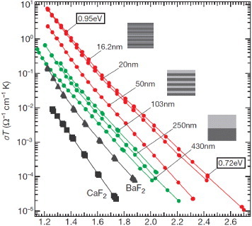
In a seminal study, Sata et al [Citation17] found that an increase in the interface density in a multilayered calcium fluoride and barium fluoride (CaF2/BaF2) strongly enhanced the ionic conductivity along the interfacial direction, particularly when the film thickness ranged between 20 and 100 nm, as compared with either bulk calcium fluoride or bulk barium fluoride (figure ). The authors attributed this conductivity enhancement to the presence of space charge regions at the interfaces.
Figure 1 Sata et al observed higher ionic conductivity in BaF2/CaF2 multilayers than in either bulk BaF2 or CaF2 along the interfacial directions. Here conductivity values are shown for multilayers with various interfacial densities, i.e. with the individual layer thickness in the 16–430 nm range, keeping the total thickness constant at about 500 nm [Citation17]. (Reproduced with permission from [Citation17] © 2000 Nature Publishing Group.)
An important theoretical model of space charge effects has been proposed by Wagner [Citation18] and Maier [Citation15, Citation19–22]. The space charge concept was introduced as one of the possible origins of the high conductivity at the interface regions due to a high concentration of mobile point defects. However, heterostructures made of doped oxides build up very narrow space charge regions; thus, the additional accumulation of charge carriers at the space charge regions, compared with the large bulk defect concentration, cannot significantly affect the total conductivity. For these heterostructures, structural effects induced by the lattice mismatch between two different phases might be responsible for the conduction in the interfacial region.
Modern thin film growth technologies are rather sophisticated and allow controlling the individual layers in a heterostructure at an atomic level, which is crucial for understanding interfacial phenomena. A thin film can also be considered as a heterostructure at the interface with the substrate, and indeed, the first evidence of interfacial effects on ionic conductivity of oxide electrolytes was derived from the study of ultra-thin films [Citation23, Citation24]. However, in a single thin film, the conduction paths along the free surface (film/gas interface) can hamper the interpretation of electrical conductivity measurements, leading to an incorrect understanding of the influence of the film/substrate interface on the ionic conductivity of the film. Moreover, the choice of the substrate plays an important role in the interface effects on the ionic conductivity, as it affects strain in the film.
In this work, we review the role of interfaces in the ionic conductivity of oxide heterostructures. As discussed below, different mechanisms can affect the electrical conductivity in interfacial regions, such as a structural mismatch between the two adjacent phases, which results in a strong defective structure with fast ionic migration, and the formation of a space charge region with an increased concentration of mobile point defects. In addition to oxide heterostructures, the interfacial effects in ion-conducting single-layer thin films are described for various substrates.
Mechanisms of ionic conductivity at oxide interfaces
Effect of space charge regions on the interfacial ionic conductivity
In ionic solids, crystalline symmetry is broken at interfaces between two grains (homophase interface) or between two different phases (heterophase interface), resulting in a local space charge region due to the redistribution of ionic and electronic defects [Citation25]. Ionic defects from the bulk phases adjacent to the interface are depleted in the space charge region, while those with opposite charge are accumulated [Citation21]. In the case of an oxygen-ion conductor with Frenkel equilibrium for the anionic sublattice, segregation of interstitial oxygen ions at the phase boundary increases the concentration of oppositely charged point defects (oxygen vacancy) in the space charge region. In contrast, in a solid with a high concentration of oxygen vacancies, such as polycrystalline yttria-stabilized zirconia (YSZ) or Gd-doped CeO2 (GDC), the grain boundaries have excessive positive charge (oxygen vacancy and electron holes), and therefore, accumulate electrons at the space charge region [Citation26–28].
The charge carrier profile in the space charge region is described by the space charge potential ΔΦ. The Boltzmann statistics can be applied to materials with sufficiently dilute point defects [Citation29] and the concentration profile for the j species between two locations can be determined by solving the spatial variation of the electrical potential, which is described by the Poisson–Boltzmann differential equation as follows [Citation5]:
1 Here qj is the net charge, cj∞ is the bulk concentration, ε0 is the permittivity of free space, εr is the relative dielectric constant, k is the Boltzmann constant and T is the absolute temperature.
The charge carrier profile described by (Equation11 ) depends on the charge carrier mobility [Citation29]. When all defect species have sufficiently high mobilities to redistribute in the space charge regions, the Gouy–Chapman conditions can be applied, for which the extension of the space charge region is of the same order as the Debye length, LD [Citation21]:
2
When the defects controlling the Debye length are insufficiently mobile to redistribute in the space charge layer in response to the excess grain-boundary charge, the depleted defects in the Poisson–Boltzmann differential equation can be neglected, and the equation is governed only by the concentration of species j:
3
Therefore, the Poisson–Boltzmann differential equation can be simplified using the Mott–Schottky approximation, leading to a space charge layer width that is dependent on the space charge potential [Citation30]:
4 where ΔΦ(0) is the potential at the interface.
The Gouy–Chapman analysis shows that the space charge layer has approximately the same extent as the Debye length, and there is generally a significant change in the concentration of charged defects within a few nanometers from the interface. Differently, under the Mott–Schottky conditions, the space charge region is much wider than the Debye length, but the change in the charge carrier concentration is less pronounced.
For a polycrystalline sample, the space charge effects significantly contribute to the total conductivity if the grain size approaches LD, such as in nanocrystalline solids [Citation16]. For heterostructures, the space charge region contributes to the total conductivity when the individual layer thickness is on the order of LD. Moreover, if the interface width is smaller than the effective width of the space charge layer, the sample is charged throughout due to space charge overlapping in different layers [Citation17].
Equations (Equation22 ) and (Equation4
4 ) show that the space charge width is inversely proportional to the square root of the concentration of point defects in the bulk materials. Therefore, heavily doped ionic conductors (i.e. the conventional SOFC electrolytes) have a narrow space charge region that does not appreciably affect the overall conductivity. For example, the Debye length for 8 mol% yttria-stabilized zirconia (YSZ) was estimated as 1 Å at 500 °C within the Gouy–Chapman conditions [Citation29]. Using the Mott–Schottky approximation and a value for the space charge potential of 0.25 eV [Citation30], the space charge layer length was estimated as 4 Å, which is still too narrow to significantly affect the YSZ transport properties, even when the film is only several nanometers thick [Citation29]. Thus, the space charge region effect can be pronounced only for materials with a low concentration of mobile point defects, which have a significantly extended Debye length.
To ensure high ionic conductivity, oxide materials are generally heavily doped with lower valence elements. This creates a high oxygen vacancy density as a consequence of charge balance. The space charge effect was claimed as the main reason for the enhanced conductivity in BaF2/CaF2 multilayers [Citation17], because of the low bulk concentration of defects, and thus, the relatively extended space charge region. However, in ion-conducting oxide heterostructures, the narrow space charge region should play a minor role in conducting properties. Undoped ionic conductors with low intrinsic defect concentration have to be used to identify the space charge effect in oxide heterostructures. While a very low conductivity is expected from undoped oxides, the creation of a space charge region with a high concentration of defects at the interfaces may lead to unexpected conductivity.
Effect of the structural mismatch on the interfacial ionic conductivity
In a heterostructure, the interface between different layers is likely strained due to the different lattice parameters and symmetries of the two adjacent phases. This strain can be relieved by mismatch dislocations, which can organize themselves and create a regular network at the interface [Citation16]. Such effects are expected to have a stronger influence on the ionic conductivity than the space charge regions.
Korte and co-workers provided a comprehensive description of the effect of structural mismatch on the interface conduction [Citation31–34]. Depending on the mismatch degree between the two adjacent phases, the interface can be classified as coherent, semicoherent or incoherent. Generally, for interfaces that are not twisted or tilted, increasing the lattice mismatch between the adjacent phases results in a change from a coherent to an incoherent interface, as illustrated in figure .
Figure 2 Sketch representing a simplified dependence of the interface structure on the lattice mismatch (f) between the adjacent layers proposed by Korte et al [Citation32]. (Reproduced with permission from [Citation32] © 2008 the PCCP Owner Societies.)
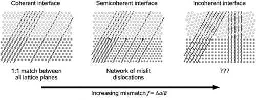
Incoherent interfaces are formed between materials with different symmetries and incommensurable lattice parameters, resulting in highly distorted or even partially amorphous interfaces. Misfit dislocations are created to accommodate the interfacial strain caused by the large mismatch. This lower packing density region, compared with the bulk, can act as a diffusion pathway for ionic conduction [Citation31]. At a semicoherent interface, misfit dislocations are arranged in a regular network, which can still provide a pathway for a faster ionic conduction than in the bulk. Coherent interfaces can be formed for a small mismatch, when the adjacent phases possess similar symmetry and commensurable lattice parameters. In this case, the mismatch is completely compensated by the elastic strain, and the ionic mobility of the interface, as a consequence, can only be affected by the strain and not by the formation of a dislocation network [Citation31, Citation32].
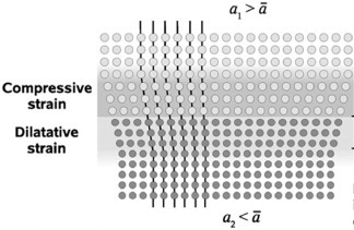
Only for a coherent interface the lattice strain (ε) can be directly correlated to the lattice misfit (f) between the adjacent layers. The lattice strain relative to phase 1 is, thus, given as
5 where a1 and a2 are the lattice parameters of phases 1 and 2, respectively.
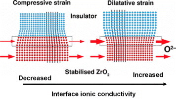
When a1 is larger than a2, there will be compressive strain in the crystallites of phase 1 and dilatative strain in the crystallites of phase 2, as shown in figure .
Figure 3 Strain field in a coherent interface. Phase 1 has a larger lattice parameter (a1) than phase 2 (a2), resulting in a compressive strain for phase 1 and a dilatative strain for phase 2 [Citation32]. (Reproduced with permission from [Citation32] © 2008 the PCCP Owner Societies.)
The strain distribution among the adjacent materials largely depends on their elastic constants. In contrast, the distribution of the strain formed at the interface depends on the crystallite size in the individual layers. For a thin, nearly single-crystal layer, the strain will be distributed over the entire layer. Similarly, layers with columnar grains, which have the dimension perpendicular to the interface smaller than the extent of the phase boundary, are almost fully strained. On the contrary, thick layers or films with columnar grains, which have the grain boundaries significantly larger than the phase boundary, will not be homogeneously strained because of mechanical relaxation [Citation32, Citation35, Citation36]. This should be taken into account when correlating the interface strain with the ionic conductivity, as a high density of grain boundaries affects not only the total conductivity but also the extension of the strained interfacial region.
Heterostructures reduced at minimum: single thin films
Although only one solid/solid interface is present for thin films deposited on a substrate, the interfacial contribution to the ionic conductivity could become dominant when the film thickness is reduced to few tens of nanometers. However, the influence of conduction pathways along the film/atmosphere interface cannot be neglected without diverting the interpretation of the enhanced conductivity at the film/substrate interface. Here, we review only some results of particular relevance obtained for ultra-thin films.
Kosacki et al deposited epitaxial YSZ thin films by pulsed laser ablation on (001)-oriented single crystals of MgO. They reported high ionic conductivity for YSZ films thinner than 60 nm. In particular, when the YSZ thickness decreased from 60 to 15 nm, the conductivity at 400 °C increased about 150 times [Citation23, Citation24]. The increase was attributed to a highly conductive layer at the YSZ/MgO interface, about 1.6 nm thick, given that the enhancement in conductivity occurred only for films thinner than 60 nm. The estimated interfacial conductivity is more than three orders of magnitude higher than the YSZ bulk conductivity [Citation24]. The activation energy decreased from 1.09 to 0.62 eV when the YSZ thickness was reduced from 60 to 15 nm. The lattice mismatch at the YSZ/MgO interface is very large (∼18%), and thus, it is expected to be compensated not only by the elastic strain but also by the formation of misfit dislocations. However, the authors presented little evidence of a dislocation network at the interface, even though Korte et al [Citation34] later revisited the TEM images of Kosacki et al and suggested the formation of a semicoherent interface with a network of dislocations that accommodated part of the lattice mismatch.
Sillassen et al also grew epitaxial YSZ films on MgO with thickness below 420 nm using reactive dc magnetron sputtering [Citation37]. Misfit dislocations at the YSZ/MgO interface were observed, in contrast to the work of Kosacki et al [Citation23]. A very high conductivity of 1 S cm−1 at 500 °C, claimed to be purely ionic, was reported for a 58-nm-thick YSZ film. The authors ruled out that the measured conductivity was influenced by the film/atmosphere interface because the conductivity of the epitaxial YSZ films decreased when strontium titanate was used as a substrate instead of MgO. However, the authors did not mention the significant thickness difference between the YSZ films grown on SrTiO3 and MgO.
Guo et al prepared polycrystalline YSZ films with a columnar structure by pulsed laser deposition (PLD) on single crystals of MgO. The film thickness ranged between 12 and 25 nm and the interface between the film and the substrate appeared highly disordered [Citation38]. The authors stated that, owing to the high lattice mismatch between the two phases, it is not possible to grow epitaxial YSZ films on MgO. The conductivity was smaller by a factor of 4 for thin nanostructured YSZ films than microcrystalline ceramics and it was independent of the film thickness. Based on these results, the authors concluded that in this case the YSZ/MgO interface did not play a significant role in the ionic conduction of the film.
Karthikeyan et al also deposited polycrystalline YSZ films of 17–210 nm thickness on single-crystal MgO substrates by electron beam evaporation [Citation39]. They observed an increase in conductivity by one order of magnitude with decreasing film thickness, but no change in activation energy. Moreover, the same enhancement in conductivity was observed when using (0001)-oriented Al2O3 substrates. The authors suggested that, owing to the small film thickness, the formation of a space charge region was the most probable reason for the conductivity increase.
GDC films with a columnar structure and 170 nm thickness were epitaxially grown on MgO (001) single crystals by pulsed laser ablation [Citation40]. The large lattice mismatch of 28.8% created various defects at the film/MgO interface, as verified by high-resolution transmission electron microscopy (HRTEM). Furthermore, to accommodate the large strain, the GDC lattice planes were tilted from the lattice planes of the MgO substrate. Lower conductivity was observed for thin films than for bulk polycrystalline GDC. Interestingly, after being exposed for a long time to high temperatures, the film showed higher conductivity and lower activation energy (0.74 eV versus 0.86 eV). The authors suggested that annealing partly reduced strain and removed some dislocations, and that this was the reason for the enhanced conductivity. Differently, Suzuki et al measured the ionic conductivity of nanocrystalline GDC films deposited on sapphire and observed a slight increase in conductivity when the film thickness (grain size of 20 nm) was decreased from 630 to 110 nm [Citation41]. Huang et al observed an increase in conductivity of about two orders of magnitude when decreasing the thickness of nanocrystalline GDC films from 500 to 20 nm [Citation42]. They fabricated the films by dc sputtering on Si wafers coated with 50-nm-thick silicon nitride and 200-nm-thick Pt layers, and deposited small Pt pads on top of the GDC films. To explain the high conductivity of the GDC layers, the authors proposed a model based on defect and dopant association. They suggested that the dopant segregation results in a region with a high oxygen-vacancy concentration that can act as a fast conduction path for ions.
Epitaxially oriented, 68-nm-thick CeO2 films were grown on (0001) sapphire by Tsuchiya et al [Citation43] and misfit dislocations were observed at the CeO2/Al2O3 interface by TEM. Ionic conduction was found for an extended range of oxygen partial pressures. The authors assumed that 1% of the oxygen sites are vacant at the CeO2/Al2O3 interface due to dislocation formation, and this allows oxygen-ion conduction down to lower pO2 as compared with thick CeO2 films. Therefore, they concluded that the existence of extended defects at the interface plays an important role in determining the ionic conduction of CeO2.
Heterostructures coupling an ionic conductor with an insulator
Korte, Janek and co-workers reported the effect of interfaces on the ionic conductivity of heterostructures composed by an ionic conducting phase and an insulator phase. They investigated the ionic conduction in heterophase boundaries between cubic stabilized zirconia and different insulating oxides, aiming to correlate the interfacial contribution to the multilayer ionic conductivity with the microstructure of the interfaces [Citation31–34]. The authors considered only structural effects to explain the conductivity in the multilayers, as compared with the conductivity for the bulk materials. They neglected the space charge region effect because of the small Debye length in doped zirconia.
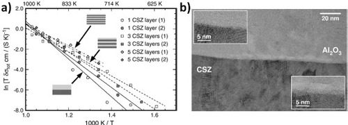
Figure shows their results for heterostructures of Ca-stabilized zirconia (CSZ) and Al2O3 [Citation31]. Pulsed laser deposition of the CSZ/Al2O3 heterostructures on single-crystal Al2O3 resulted in polycrystalline CSZ layers with a columnar microstructure and amorphous alumina layers. They crystallized only after annealing at 800 °C, revealing randomly oriented CSZ columns and Al2O3 grains and indicating the formation of incoherent interfaces (figure (a)). When increasing the number of interfaces to 5, an increase of about two orders of magnitude was recorded in the low-temperature ionic conductivity of the heterostructure with respect to oxygen-ion CSZ bulk conductivity, as shown in figure (b). Furthermore, a strong decrease in the activation energy of about 0.5 eV was observed with increasing the number of interfaces. The enhancement in conductivity and the decrease in activation energy were attributed to the pronounced disorder at the incoherent CSZ/Al2O3 interfaces, which enhances ionic mobility at the interface core regions.
Figure 4 Arrhenius plot of the total conductivity of CSZ/Al2O3 heterostructures with different numbers of interfaces (a). HRTEM micrograph of a CSZ/Al2O3 interface and magnifications of selected regions (b); top left inset: regular phase boundary, bottom right inset: pores in alumina at the interface [Citation31]. (Reproduced with permission from [Citation31] © 2007 Elsevier Publishing Group.)
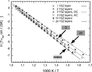
In a more recent paper, the same group reported the effect of the interface density on the conductivity in an YSZ/Y2O3 multilayer [Citation32]. In this case, the mismatch between the oxides in the multilayer is relatively small (about 3%) and a semicoherent interface with low density of misfit dislocations was obtained. PLD was used to fabricate the multilayer on (0001)-oriented single-crystal Al2O3 substrates, and Y2O3 was used as the first and the last layer to guarantee that only YSZ/Y2O3 interfaces were present within the multilayer. The YSZ and Y2O3 layers were mostly epitaxial and (111) oriented, with columnar grains of 60–100 nm oriented perpendicular to the substrate. The thickness of the individual YSZ layer was varied from 260 to 24 nm, keeping the total stack thickness constant. An increase in conductivity by a factor of 1.4 and a decrease in activation energy were observed with increasing the number of interfaces to 20, as shown in figure .
Figure 5 Arrhenius plot of the total conductivity of YSZ/Y2O3 multilayers with different numbers of interfaces [Citation32]. (Reproduced with permission from [Citation32] © 2008 the PCCP Owner Societies.)
When the heterostructure layers have a columnar microstructure, there are at least three ion conduction pathways: through the bulk, along the interfaces, and along or across the grain boundaries. The last mechanism can be blocking or providing an additional fast pathway for ions. Furthermore, in a columnar structure, the grain dimension perpendicular to the phase boundary might exceed the dimension of the phase boundary leading to an inhomogeneous strain field and a strain relaxation along the grain. For the YSZ/Y2O3 multilayer, HRTEM demonstrated that the misfit dislocations at the semicoherent interfaces did not form a periodic alignment, probably because grains with large grain boundaries can absorb more elastic energy than crystallites with a small ratio of grain boundary length to phase boundary length. Considering the low density of misfit dislocations at the YSZ/Y2O3 interfaces, the authors concluded that the interface conduction was mainly governed by the elastic strain rather than fast transport along the network of misfit dislocations [Citation34].
Korte and co-workers also proposed a qualitative model for the ionic transport along heterophase interfaces, based on the density of misfit dislocations and the interfacial strain [Citation33, Citation34]. For an oxygen-ion conductor with oxygen vacancy charge carriers (positive migration volume), the pressure dependence of the interface conductivity on the free molar migration volume indicates that dilatative strain (negative pressure) will increase the conductivity along the strained region, while compressive strain (positive pressure) will decrease the ionic conductivity [Citation33, Citation34]. This is consistent with a molecular dynamics study of YSZ, which indicates an increase in oxygen–ion diffusion for a film subjected to dilatative strain [Citation44]. Furthermore, this model predicts a linear dependence of the interfacial conductivity on the lattice mismatch, as shown in figure ; with increasing the dilatative strain, and consequently the lattice mismatch between the adjacent phases, the interfacial conductivity linearly increases, while the activation energy decreases. However, the model proposed by Korte et al does not take into account anisotropies and stress relaxation in heterostructures. Moreover, the extension of the region with enhanced conductivity close to the interface is missing. Considering the linear dependence of the total conductivity on the reciprocal thickness of the YSZ layer, the region with enhanced conductivity is expected to be thinner than 15–20 nm [Citation34].
Figure 6 Schematic illustration of the dependence of the ionic conductivity at stabilized zirconia/insulator interfaces on the strain proposed by Korte et al [Citation34].
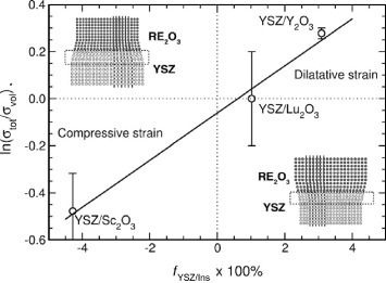
The proposed model agrees with the experiments performed by the same group. Together with the YSZ/Y2O3 and CSZ/Al2O3 multilayers discussed above, the authors also investigated the role of interfaces in the ionic conductivity of YSZ/Lu2O3 and YSZ/Sc2O3 multilayers. All the studied multilayers showed semi-coherent or quasi-coherent interfaces, except for CSZ/Al2O3 multilayers that had incoherent interfaces as described above. The lattice mismatches are 3.09%, 1.02% and −4.28% (compressive strain) for YSZ/Lu2O3, YSZ/Y2O3 and YSZ/Sc2O3 multilayers, respectively. YSZ/Lu2O3 showed coherent interfaces with almost no mismatch dislocations, while some dislocations with an irregular arrangement were observed for YSZ/Y2O3 and YSZ/Sc2O3 semicoherent interfaces. According to the proposed model, the conductivity was smaller for YSZ/Sc2O3 multilayer (N=20 interfaces) than for bulk YSZ, while no significant change in conductivity was observed for the YSZ/Lu2O3 heterostructure when increasing the interface density. Finally, a higher conductivity was revealed for YSZ/Y2O3 than for bulk YSZ, as illustrated above. Also, the trend of the activation energy fulfills the model prediction: the activation energy, with respect to the YSZ bulk, increased by about 0.1 eV for the YSZ/Sc2O3 multilayer (compressive strain), it was nearly unchanged for the YSZ/Lu2O3 multilayer and decreased by about 0.13 eV for the YSZ/Y2O3 multilayer (dilatative strain). For the YSZ/Al2O3 heterostructures with highly structural disordered interfaces, the measured effect on the conductivity and activation energy was much stronger than for YSZ/Y2O3, with a further enhancement in conductivity and a decrease in the activation energy. Therefore, the authors concluded that the heterostructures with the largest mismatch between the adjacent layers or with incoherent interfaces should have the highest interfacial conductivity and the lowest activation energy. Figure shows the logarithm of the ratio between the multilayer and the bulk YSZ conductivities as a function of the mismatch (and thus the strain). For coherent interfaces, the interface transport is mostly dominated by elastic strain, while atomic packing density and misfit dislocation density govern the conductivity at incoherent interfaces.
Figure 7 Plot of the conductivity enhancement in the YSZ/RE2O3 structure (RE2O3=Sc2O3, Lu2O3 or Y2O3) as a function of the mismatch factor for the YSZ layer [Citation33]. (Reproduced with permission from [Citation33] © 2009 the PCCP Owner Societies.)
Garcia-Barriocanal et al investigated the conductivity of epitaxial trilayer YSZ/SrTiO3 heterostructures grown on (001) SrTiO3 single crystals. They varied the YSZ thickness between 1 and 62 nm while keeping the SrTiO3 thickness constant at 10 nm [Citation45]. The thinnest YSZ showed coherent interfaces, while increasing the YSZ thickness resulted in a loss of structural coherence. A colossal increase in conductivity, of about eight orders of magnitude, was reported for the multilayer with 1-nm-thick YSZ layers. The conductivity was found to increase with increasing the number of interfaces, but it was almost independent of the YSZ layer thickness. This finding was interpreted as a proof that the measured conductivity was based on interfacial processes. The major experimental evidence for the ionic character of the conductivity was that the dc conductivity was several orders of magnitude lower than the ac conductivity. A decrease in the activation energy was reported with decreasing YSZ thickness. The large conductivity increase was explained by a high concentration of oxygen vacancies at the interface, induced by the lattice mismatch between the adjoining lattice phases and the concomitant atomic reconstruction. It should be pointed out that the authors calculated the conductivity only taking into account the total YSZ thickness, neglecting the contribution of the SrTiO3 layers/substrate. Although the authors claimed that the measured conductivity was purely ionic, this was questioned because of the much smaller conductivity increase observed by other groups [Citation33, Citation34, Citation46, Citation47]. Schichtel et al calculated a maximum increase in ionic conductivity of about 2.5 orders of magnitude in the ideal case where all the elastic strain caused by the lattice mismatch between YSZ and SrTiO3 (f=7.37%) is concentrated in the YSZ layers and there is no strain release [Citation33]. Guo pointed out that, since SrTiO3 is a p-type conductor in oxidizing atmospheres, the contribution of the SrTiO3 substrate and of the 10-nm-thick layers to the heterostructure conductivity cannot be ignored [Citation46]. In fact, if the SrTiO3 substrate and layer thicknesses are taken into account, then the reported conductivity decreases by six orders of magnitude. Furthermore, the reported activation energy for the YSZ/SrTiO3 heterostructure (0.64 eV) [Citation45] is close to the activation energy measured for the SrTiO3 substrate (0.66 eV) [Citation46]. More recently, Cavallaro et al measured the conductivity dependence on the oxygen partial pressure and the oxygen diffusion by means of tracer experiments in YSZ/SrTiO3 heterostructures, and suggested that the main contribution to the conductivity reported in [Citation45] was related to electrons rather than ions [Citation47]. They reported that 1 nm thick YSZ layers were discontinuous and consisted of island exhibiting a range of different tilt and orientation relationships to the SrTiO3 substrate. The measured dependence of the conductivity on the oxygen partial pressure with an exponent of 1/4 and the lack of 18O diffusion along the interfaces were reported as unequivocal proofs of the electronic conductivity in the YSZ/SrTiO3 heterostructures [Citation47].
Kuwata et al fabricated epitaxial SrZr0.95Y0.05O3-δ(SZY)/SrTiO3 superlattices by PLD [Citation48, Citation49]. The authors selected (001)-oriented MgO substrates because of their insulating properties. TEM revealed that the superlattice layers were homogeneous and dense, with columnar structure and sharp and clean interfaces. No misfit dislocations were observed between SZY and SrTiO3 layers in an earlier work, and it was claimed that the lattice mismatch (5%) was accommodated by the elastic strain [Citation48]. However, misfit dislocations at the SZY/SrTiO3 interface were observed later [Citation49]. In-plane conductivity measurements revealed one order of magnitude higher conductivity for a superlattice with a SZY/SrTiO3 double layer of 1.2 nm in thickness than for an epitaxial SZY single layer grown on MgO. The conductivity gradually increased with increasing the number of interfaces, but no change in activation energy was observed [Citation49]. By substituting D2O for H2O, it was confirmed that protons do contribute to the superlattice conductivity [Citation48]; they are probably not the only charge carriers, as the conductivity ratio in H2O and D2O atmospheres (σH2O/σD2O) was smaller than the expected value of 21/2 [Citation50]. Although the conductivity nature of the superlattices was not fully clarified, the authors assumed that the enhanced conductivity was due to interfacial effects. In particular, they suggested that an increase in the defect density due to the interfacial strain is the main cause of the increased conductivity.
Heterostructures of two ion-conducting oxides
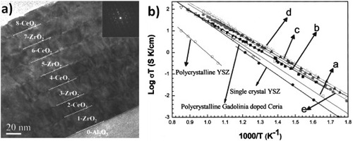
Azad et al investigated the conductivity dependence on the film thickness in a structure consisting of Gd-doped CeO2 and ZrO2 layers deposited by oxygen plasma-assisted molecular beam epitaxy on an (0001) Al2O3 substrate [Citation51]. TEM observations (figure (a)) revealed dislocations both at the interface and in the layers, regardless of the number of interfaces. However, the dislocations at the interfaces were separated by a distance much longer than expected considering the lattice mismatch between the two phases. The authors explained this finding considering the highly textured structure of the layers (epitaxially (111)-oriented) and that the lattice misfit was also accommodated by the dislocations formed in the layer bulk. They reported a conductivity increase of about one order of magnitude with increasing the number of interfaces (figure (b)), i.e. decreasing the thickness of the layers down to 15 nm and keeping the total thickness constant. However, the conductivity decreased for the layer thickness below 15 nm. The authors interpreted their observations in terms of the lattice strain and extended defects due to lattice mismatch.
Figure 8 TEM micrograph showing a cross-sectional view of an eight-layer Gd2O3-doped CeO2 and ZrO2 film grown on Al2O3 (0001) (a). Arrhenius plots of oxygen-ion conductivity in 2- (a), 4- (b), 8- (c), 10- (d), and 16-layer (e) gadolinia-doped ceria-zirconia thin films. The data from polycrystalline and single-crystal YSZ are also displayed [Citation51]. (Reproduced with permission from [Citation51] © 2005 American Institute of Physics Publishing Group.)
Sanna et al investigated the electrical conductivity of heterostructures consisting of 20% Sm-doped ceria (SDC) and YSZ grown by PLD on a SrTiO3 buffer layer deposited on single-crystal MgO [Citation52]. The use of SrTiO3 buffer layers allows growing thin layers with an excellent crystalline quality [Citation53]. The authors not only varied the number of interfaces (N=3, 8 and 20) at the constant total thickness of 154 nm, but also the thickness of the individual SDC/YSZ bilayers (Λ=7.7, 15 and 28 nm) keeping the number of interfaces constant at N=20. An increase in conductivity was observed with increasing the number of interfaces to N=20 and with an SDC/YSZ bilayer thickness of 7.7 nm, which is much lower than the minimum bilayer thickness at which Azad et al [Citation51] observed a conductivity increase. In particular, one order of magnitude higher conductivity was observed for multilayers with N=20 than for single-layer SDC and YSZ thin-films deposited on SrTiO3-buffered MgO. Reciprocal space mapping revealed increasing strain in YSZ layers with reducing the bilayer thickness for Λ below 28 nm. The conductivity dependence on the oxygen partial pressure indicated that the main contribution to the measured conductivity was ionic. In contrast to the other results on ionic conductor/insulator heterostructures, for the SDC/YSZ samples, the activation energy increased from 0.76 to 1.093 eV with increasing the number of interfaces.
Final remarks
The electrical properties of oxides can be effectively tuned by interfacial design and it is possible to increase the conductivity of ion-conducting oxides by designing heterostructures. Despite considerable attention to ionic conductivity in oxide heterostructures, the charge transport along their interfaces is not completely understood yet. In the case of doped oxides, the enhancement of heterostructure conductivity with respect to the bulk materials cannot be explained merely by the formation of space charge regions at the interfaces, and the structural effects due to the lattice mismatch have to be taken into account.
The growing device miniaturization will lead to a substantial impact of interfaces on the overall ionic transport in solid-state ionic devices. Therefore, the field of ionically conducting heterostructures is expected to play a substantial role in future materials research. Much experimental and theoretical work is needed to explore the full potential of interface ionic conductivity in oxide heterostructures.
References
- CatlowJ TDeasleyP JOwenS J TWebbP W 1967 J. Mater. Sci. 2 88 http://dx.doi.org/10.1007/BF00550056
- ReyrenN et al 2007 Science 317 1196 http://dx.doi.org/10.1126/science.1146006
- O'DonnellJAndrusA EOhSCollaE VEcksteinJ N 2000 Appl. Phys. Lett. 76 1916
- GuoXMaierJ 2009 Adv. Mater. 21 2629
- TullerH LLitzelmanS JJungW 2009 Phys. Chem. Chem. Phys. 11 3023 http://dx.doi.org/10.1039/b901906e
- KilnerJ A 2008 Nat. Mater. 7 838 http://dx.doi.org/10.1038/nmat2314
- GerhardtRNowickA SMochelM EDumlerI 1986 J. Am. Ceram. Soc. 69 641 http://dx.doi.org/10.1111/j.1151-2916.1986.tb07464.x
- BadwalS P SRajendranS 1994 Solid State Ion. 70–71 83 http://dx.doi.org/10.1016/0167-2738(94)90291-7
- AokiMChiangY MKosackiILeeJ RTullerH LLiuY J 1996 J. Am. Ceram. Soc. 79 1169 http://dx.doi.org/10.1111/j.1151-2916.1996.tb08569.x
- LiangC CMalloryP R 1973 J. Electrochem. Soc. 120 1289 http://dx.doi.org/10.1149/1.2403248
- GuptaR KAgrawalR C 1994 Solid State Ion. 72 314 http://dx.doi.org/10.1016/0167-2738(94)90166-X
- LeeJ SAdamsSMaierJ 2000 Solid State Ion. 136 1261 http://dx.doi.org/10.1016/S0167-2738(00)00583-X
- RizeaAChirlesanDPetotCPetot-ErvasG 2002 Solid State Ion. 146 341 http://dx.doi.org/10.1016/S0167-2738(01)01024-4
- YamadaHBhattacharyyaA JMaierJ 2006 Adv. Funct. Mater. 16 525 http://dx.doi.org/10.1002/adfm.200500538
- MaierJ 1995 Prog. Solid State Chem. 23 171 http://dx.doi.org/10.1016/0079-6786(95)00004-E
- TullerH T 2000 Solid State Ion. 131 143 http://dx.doi.org/10.1016/S0167-2738(00)00629-9
- SataNEbermanKEberlKMaierJ 2000 Nature 408 946 http://dx.doi.org/10.1038/35050047
- JiangSWagnerJ B 1995 J. Phys. Chem. Solids 56 1101 http://dx.doi.org/10.1016/0022-3697(95)00025-9
- SataNJin-PhilippN YEberlKMaierJ 2002 Solid State Ion. 154–155 497 http://dx.doi.org/10.1016/S0167-2738(02)00488-5
- MaierJ 2002 Solid State Ion. 148 367 http://dx.doi.org/10.1016/S0167-2738(02)00075-9
- MaierJ 2003 Solid State Ion. 157 327 http://dx.doi.org/10.1016/S0167-2738(02)00229-1
- MaierJ 2004 Solid State Ion. 175 7 http://dx.doi.org/10.1016/j.ssi.2004.09.051
- KosackiIRouleauC MBecherP FBentleyJLowndesD H 2004 Electrochem. Solid-State Lett. 7 A459 http://dx.doi.org/10.1149/1.1809556
- KosackiIRouleauC MBecherP FBentleyJLowndesD H 2005 Solid State Ion. 176 1319 http://dx.doi.org/10.1016/j.ssi.2005.02.021
- MaierJ 2005 Nat. Mater. 4 805 http://dx.doi.org/10.1038/nmat1513
- ChiangY-MLavikEKosackiITullerH LYingJ Y 1996 Appl. Phys. Lett. 69 185 http://dx.doi.org/10.1063/1.117366
- TschöpeASommerEBirringerR 2001 Solid State Ion. 139 255 http://dx.doi.org/10.1016/S0167-2738(01)00678-6
- KimSMaierJ 2002 J. Electrochem. Soc. 149 J73 http://dx.doi.org/10.1149/1.1507597
- MaierJ 2004 J. Electrochem. Soc. 13 593
- LitzelmanS JHertaJ LJungWTullerH L 2008 Fuel Cells 5 294 http://dx.doi.org/10.1002/fuce.200800034
- PetersAKorteCHesseDZakharovNJanekJ 2007 Solid State Ion. 178 67 http://dx.doi.org/10.1016/j.ssi.2006.12.004
- KorteCPetersAJanekJHesseDZakharovN 2008 Phys. Chem. Chem. Phys. 10 4623 http://dx.doi.org/10.1039/b801675e
- SchichtelNKorteCHesseDJanekJ 2009 Phys. Chem. Chem. Phys. 11 3043 http://dx.doi.org/10.1039/b900148d
- KorteCSchichtelNHesseDJanekJ 2009 Monatsh. Chem. 140 1069 http://dx.doi.org/10.1007/s00706-009-0125-7
- PeopleRBeanJ C 1985 Appl. Phys. Lett. 47 322 http://dx.doi.org/10.1063/1.96206
- LuryiSSuhirE 1986 Appl. Phys. Lett. 49 140 http://dx.doi.org/10.1063/1.97204
- SillassenMEklundPPrydsNJohnsonEHelmerssonUB⊘ttigerJ 2010 Adv. Funct. Mater. 20 2071 http://dx.doi.org/10.1002/adfm.201000071
- GuoXVascoEMiSSzotKWachsmanEWaserR 2005 Acta Mater. 53 5161 http://dx.doi.org/10.1016/j.actamat.2005.07.033
- KarthikeyanAChangC HRamanathanS 2006 Appl. Phys. Lett. 89 183116 http://dx.doi.org/10.1063/1.2385211
- ChenLChenC LChenXDonnerWLiuS WLinYHuangD XJacobsonJ 2003 Appl. Phys. Lett. 83 4737 http://dx.doi.org/10.1063/1.1629378
- SuzukiTKosackiIAndersonH U 2002 Solid State Ion. 151 111 http://dx.doi.org/10.1016/S0167-2738(02)00589-1
- HuangHGurT MSaitoYPrinzF 2006 Appl. Phys. Lett. 88 143107 http://dx.doi.org/10.1063/1.2358851
- TsuchiyaMBojarczukN ARamanathanS 2007 Appl. Phys. Lett. 91 223101 http://dx.doi.org/10.1063/1.2818666
- SuzukiKKuboMOumiYMiuraRTakabaHFahmiAChatterjeeATeraishiKMiyamotoA 1998 Appl. Phys. Lett. 73 1502 http://dx.doi.org/10.1063/1.122186
- Garcia-BarriocanalJRivera-CalzadaAVarelaMSefriouiZIborraELeonCPennycookS JSantamariaJ 2008 Science 321 676 http://dx.doi.org/10.1126/science.1156393
- GuoX 2009 Science 324 465 http://dx.doi.org/10.1126/science.1168940
- CavallaroA et al 2010 Solid State Ion. 181 592 http://dx.doi.org/10.1016/j.ssi.2010.03.014
- KuwataNSataNTsuruiTYugamiH 2005 Japan J. Appl. Phys. 44 8613 http://dx.doi.org/10.1143/JJAP.44.8613
- KuwataNSataNSaitoSTsuruiTYugamiH 2006 Solid State Ion. 177 2347 http://dx.doi.org/10.1016/j.ssi.2006.05.043
- ScherbanTNowickA S 1989 Solid State Ion. 35 189 http://dx.doi.org/10.1016/0167-2738(89)90029-5
- AzadS et al 2005 Appl. Phys. Lett. 86 131906 http://dx.doi.org/10.1063/1.1894615
- SannaSEspositoVTebanoALicocciaSTraversaEBalestrinoG 2010 Small at press
- SannaSEspositoVPergolesiDOrsiniATebanoALicocciaSBalestrinoGTraversaE 2009 Adv. Funct. Mater. 19 1713 http://dx.doi.org/10.1002/adfm.200801768