
Abstract
A ternary thin film combinatorial materials library of the valve metal system Hf–Ta–Ti obtained by co-sputtering was studied. The microstructural and crystallographic analysis of the obtained compositions revealed a crystalline and textured surface, with the exception of compositions with Ta concentration above 48 at.% which are amorphous and show a flat surface. Electrochemical anodization of the composition spread thin films was used for analysing the growth of the mixed surface oxides. Oxide formation factors, obtained from the potentiodynamic anodization curves, as well as the dielectric constants and electrical resistances, obtained from electrochemical impedance spectroscopy, were mapped along two dimensions of the library using a scanning droplet cell microscope. The semiconducting properties of the anodic oxides were mapped using Mott–Schottky analysis. The degree of oxide mixing was analysed qualitatively using x-ray photoelectron spectroscopy depth profiling. A quantitative analysis of the surface oxides was performed and correlated to the as-deposited metal thin film compositions. In the concurrent transport of the three metal cations during oxide growth a clear speed order of Ti > Hf > Ta was proven.
Introduction
High-throughput experimentation is a key factor for effectively analysing combinatorial material libraries. In order to obtain reliable and reproducible results, appropriate tools must be available which, apart from having a certain degree of automation, must be adapted to the specific characteristics of each analysed library, e.g. geometric size, compositional resolution, sample thickness, etc [Citation1]. Screening for certain properties (e.g. dielectric constant) can be done in a relatively short time and results coming from analysing complex libraries (e.g. ternary or larger) can accelerate finding the optimum compositions relevant for the screened properties [Citation2].
Hf, Ta and Ti have similar electrochemical behaviour in the sense that their anodic oxidation occurs in the same manner; a strong current decrease is observed upon the electric field reversal during a potentiodynamic experiment. This valve-like behaviour led to naming this group of metals (including Al, Nb and to some extent Mo, W and Zr) valve metals [Citation3]. The valve metal oxides grow following the high-field mechanism [Citation4] and are very difficult to reduce under cathodic polarization [Citation5]. They are able to withstand an electric field equal to the film formation field strength [Citation6], may be amorphous (glassy Ta) [Citation7] and are used in various applications including orthopaedic implants and mesoporous materials [Citation8, Citation9].
In recent years, HfO2 started to gain increased scientific interest especially for its use as gate material for electronic applications due to its high dielectric constant and excellent thermal stability [Citation10]. HfO2 is also a promising material for use as a carbon monoxide sensor for monitoring the completeness of combustion in flue gas, which is important for optimizing safety, efficiency and fuel consumption [Citation11]. In addition to HfO2, Ta2O5 is used in electronics for the fabrication of capacitors and high power resistors either in the form of oxidized metal powder or sputtered thin films [Citation12]. In their oxidized states, mixtures of Hf and Ta were studied as high-k gate dielectrics. Ultrathin films (below 2 nm) of Hf-doped Ta2O5 were successfully used for the fabrication of metal–oxide–semiconductor transistors [Citation13, Citation14]. Combination of HfO2 with even higher dielectric constant materials, such as TiO2 is currently a high-interest topic for electronic applications. The structure of photoinduced chemical vapour deposited (PI-CVD) TiO2-doped HfO2 thin films was investigated and evidence was found linking the degradation of the electrical properties to the presence of the crystalline anatase phase in the TiO2–HfO2 system, which in turn is responsible for high leakage current densities [Citation15]. Increased leakage currents along with an increased dielectric constant were found during the electrical characterization of HfO2/TiO2 nanolaminates, obtained by atomic layer deposition [Citation16]. Spark anodization of Ti alloys has been shown to produce highly crystalline oxides since Al ions migrating in the high electric field were found even in the inner part of the anodic films due to the electrolyte penetration to the film/substrate interface through the discharge channels [Citation17].
The effect of low Hf concentrations on the microstructure and mechanical properties of Hf–Nb–Ti ternary alloys was recently investigated. The results showed a significant increase of the tensile strength due to the presence of Hf and the alloys were considered as a favourable choice for biological applications due to a relatively low elastic modulus (65 GPa) [Citation18]. The solidification of Ni-based superalloys containing Hf, Ta and Ti was characterized in another study. The (Hf + Ta + Ti)/Al ratio in the residual liquid played a significant role in the nucleation of the η phase, which occurred as a result of segregation of alloying elements during solidification [Citation19].
In a comprehensive study of the anodization of a Hf–Ta thin film library, three different compositional zones including an amorphous region were identified when analysing the microstructure of the metallic thin films [Citation20]. Investigations of the semiconducting properties of mixed anodic oxides grown on a Hf–Ti library showed that n-type behaviour can be obtained to some extent through electrochemical anodization [Citation21]. A general tendency of the TiO2 surface enrichment during the anodization of a Ta–Ti composition spread was reported and attributed to the different ionic transport numbers of Ta and Ti, both competing during the reaction for the oxygen in the oxide formation process [Citation22]. Self-ordered formation of nanotubes was observed by anodization of various Ta–Ti alloys in H2SO4 and their morphologies were related to the metal alloy composition [Citation23].
Due to the high interest in the properties of Hf, Ta and Ti combinations of anodic oxides, anodization of a ternary Hf–Ta–Ti combinatorial library should provide further information about the mixture and combined properties of these oxides. Such information is comprehensively reported in the present work.
Experimental details
Deposition of Hf–Ta–Ti compositional spread
The Hf–Ta–Ti thin film compositional spread sample was obtained using a co-sputtering technique in an ultra-high vacuum system (DCA, Finland). All three targets, 101.6 mm in diameter, were aimed at the center of the substrate while placed 72° apart from each other. Hf and Ta were sputtered in the RF mode from high purity targets (99.995%, Kaistar R&D) using a power of 200 W, which led to deposition rates of 0.96 and 0.73 nm s−1, respectively. Due to the much lower sputter rate of Ti in the RF mode, the dc mode was used for Ti deposition (Ti 99.995%, Williams Advanced Materials), with a power of 200 W leading to a sputter rate of 0.13 nm s−1. A thermally oxidized Si wafer, 100 mm in diameter, was used as substrate for the co-sputtering deposition of the Hf–Ta–Ti combinatorial library. The concentrations of Hf, Ta and Ti in the library reached maximum values of 47, 55 and 39 at.%, respectively. For all depositions, the base pressure of the chamber was at least 2 × 10⁻⁶ Pa. The depositions were carried out at room temperature in Ar atmosphere with a pressure of 0.67 Pa. The target–substrate distances were approximately 190 mm, leading to the formation of wedge-shaped concentration gradients of each metal in the resulting thin film. The total thickness of the film was approximately 300 nm at the wafer center. Additionally, pure Hf, Ta and Ti thin films were separately deposited, using the same conditions, to serve as references for the combinatorial library. After the deposition of the compositional spread, energy dispersive x-ray spectroscopy (EDX) was used for mapping the element concentrations across the library. A precise measurement of the three concentration gradients allowed an accurate identification of the composition of various Hf–Ta–Ti alloys in the combinatorial library. More details regarding the fabrication and high-throughput characterization of thin film material libraries can be found elsewhere [Citation24, Citation25].
Microelectrochemical cell description
A 3-electrode configuration scanning droplet cell microscope (SDCM) was used for the growth and characterization of the anodic oxides on the surface of the Hf–Ta–Ti thin film materials library [Citation26]. This miniaturized type of electrochemical cell was successfully used in various studies where direct oxide writing [Citation27, Citation28] or localized anodizations on combinatorial thin film libraries [Citation20–Citation22, Citation29, Citation30] were necessary. The outer body of the cell was made from a borosilicate glass capillary having a diameter of 2.5 mm, previously tapered using a thermal puller (PC-10, Narishige). A small tip with a diameter of 200 μm was obtained using a micro-grinder (EG-400, Narishige). The reference electrode used was a capillary-based μ-AuHg/Hg2(CH3COO)2/NaCH3COO probe, having a 100 μm tip diameter [Citation31]. A 1 mm wide Au band wrapped around the reference electrode capillary was used as counter electrode and they were inserted together into the main capillary body. More details regarding the reference electrode and cell fabrication can be found in [Citation28]. A silicone seal was fabricated at the tip of the cell by immersing it into liquid silicone followed by drying in flowing nitrogen. For ensuring a reproducibly wetted surface (i.e. working electrode size) on the Hf–Ta–Ti thin films, the tip of the cell was pressed against the investigated surface with a predefined force that resulted in only an elastic deformation of the gasket. In this way, the electrolyte–air contact was avoided and the wetted area on the surface of the composition spread had a very high reproducibility. The measurement errors obtained when using the SDCM were previously analysed in a statistical investigation of oxide spots on pure Hf films and the errors were found to be less than 1% [Citation32].
Hardware description and measurement details
A 100 μl syringe was used for dosing the electrolyte from the cell in order to wet each investigated spot. A computer-controlled micro-syringe pump (Micro 4, World Precision Instruments) was used for actuating the syringe. The electrical contact to the metallic surface was achieved using a W needle in hard contact with the sample. Due to the fact that the investigated metallic alloys have graduated variations in composition across the surface of the wafer, an automated, high-throughput measurement approach was necessary. The SDCM can be positioned at various locations across the sample surface by a computer-controlled three-dimensional scanner actuating XYZ translation stages. Using a LabView control and data acquisition software developed in house, high-throughput experimentation was achieved. Details about the software can be found in [Citation28]. A force sensor (KD45 2N, ME-Messsysteme) combined with a lock-in amplifier (EG&G 7265) were involved in the automated control of the applied force for pressing the tip of the microelectrochemical cell against the sample. The microstructure of the Hf–Ta–Ti thin films was characterized by scanning electron microscopy (SEM, Zeiss LEO1550 VP) and 1° grazing incidence x-ray diffraction (GIXRD, Bruker AXS D8, Cu Kα) at selected locations chosen from the EDX mappings which correspond to different compositions and morphologies. The surface was locally anodized in an acetate buffer electrolyte (pH 6.0) prepared from p.a. chemicals and de-ionized water using a potentiostat (Solartron Schlumberger Electrochemical Interface 1287). Small oxide spots were locally grown at 69 different locations, uniformly distributed across the surface of the Hf–Ta–Ti library. The anodizations were carried out potentiodynamically with a potential scan rate of 100 mV s−1. Cyclic voltammograms with the upper potential limit ranging between 1 and 10 V were sequentially recorded in 1 V steps for each investigated spot. Before each cyclic voltammogram, the impedance of the previously formed oxide layer was measured using a frequency response analyser (S5720C, NF Electronic Instruments) with a 10 mV ac voltage perturbation. In order to determine the dielectric constant and electric resistivity of the anodic oxides in situ, the impedance was measured at high (1 kHz) and low (0.1 Hz) frequencies for calculating the capacitance and the resistance of the oxide, respectively. X-ray photoelectron spectroscopy (XPS, PHI small spot scanning ESCA, Quantum 2000) was used for the in-depth chemical analysis of the Hf–Ta–Ti library at different compositions. The XPS peak identification and analysis was performed using the MultiPak Database, (Data Reduction Software for AES and XPS, Version 6—Physical Electronics).
Results and discussion
Microstructure of Hf–Ta–Ti thin films
The surface structure of the Hf–Ta–Ti thin films was analysed by SEM, with figure showing a map of the morphologies observed. The relative positions of the metallic sputtering targets are indicated in the figure and the composition of each investigated region is given. In the Ti-rich region of the materials library, similar features were observed between various SEM measurement regions (zones). For Ti concentrations ranging from 37 to 39 at.% in the top line of SEM images, slightly elongated grains can be observed forming a compact metallic surface. Distinct ellipsoidal grains with a long axis of approximately 100 nm and well-defined grain boundaries can be observed randomly oriented on the surface. In the second line of SEM images from figure where the Ti concentration has decreased by about 10%, the surface microstructure slightly changes. There is a pronounced elongation of the grains on the left side of this row where there is a higher amount of Ta (41–44 at.%), whereas the shape and size of the grains become more uniform on the right side with higher Hf contents.
Figure 1 SEM images of the Hf-Ta-Ti thin films. The relative positions of Hf, Ta and Ti sputtering sources are indicated.
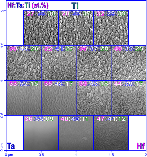
In the Ta-rich compositional region (lower left corner of figure ), the grain structure goes through a continuous, gradual transformation. Longer and less visible grains are present for Ta concentrations around 50 at.% and surface features can no longer be observed once 55 at.% Ta concentration is achieved. This featureless surface is present in regions where the Hf content is also high, suggesting an amorphization of these thin films, similar to what was previously observed in a binary Hf–Ta library [Citation20]. This is an indication for the local formation of a metallic glass.
The Hf-rich compositional zone located in the lower right part of figure has a particular grain structure represented by longer grains with higher aspect ratios than the grains previously described. Long grains can be observed on the surface of the Hf–Ta–Ti thin films for the highest Hf content of 47 at.%, even though a certain degree of amorphization is suggested by the almost featureless SEM image measured for Hf40Ta49Ti11. The surface evolution of the Hf–Ta–Ti thin films shown in the last line of the SEM mapping (figure ) suggests that the amorphization is mainly caused by the increase of the Ta concentration. The same trend is observed vertically, along the Ti gradient.
In order to evaluate the crystallographic properties of the Hf–Ta–Ti thin films, XRD analysis was performed at various Hf:Ta:Ti ratios and the results are summarized in figure . The XRD patterns measured on pure Hf, Ta and Ti are shown as references. Pure Hf and Ti thin films have hexagonal symmetries while Ta shows a tetragonal structure. The evolution of the XRD patterns recorded at different compositions is rather complicated. There is no obvious symmetry group which can be attributed to the investigated compositions. Nevertheless, a remarkable peak located between 67° and 69° in the diffractograms indicates a crystalline structure. This may be attributed to the hexagonal (103) orientation due to the slight shift of the peak between the positions of Hf (103) and Ti (103) with the increase of Ti and decrease of Hf in the library. This effect was previously encountered in a fully miscible Hf–Ti combinatorial library [Citation21].
Figure 2 XRD patterns for different concentrations of the Hf–Ta–Ti library.
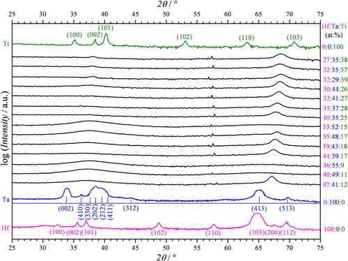
A small peak corresponding to the Hf (110) position can be observed in almost all diffractograms and its fixed position may suggest a certain degree of Hf segregation in the Hf–Ta–Ti library. The amorphization zone assumed for high Ta concentrations in figure is confirmed here by a lack of XRD peaks. For the compositions corresponding to the amorphous alloys, the XRD patterns show only very broad peaks with centres located at the position of either Ta (202) or Ti (002). If the latter suggestion is found to be true, the XRD results would suggest that the Hf–Ta–Ti alloys investigated here have hexagonal symmetry. In this case, the presence of Ta did not induce the formation of a cubic structure, as observed previously in a Ta–Ti compositional spread [Citation22], but rather an amorphization of the thin films. Along the entire Hf–Ta–Ti compositional spread, the crystalline/amorphous structures found are most likely the result of a complex mixture of various symmetries identified during the XRD analysis (figure ) and visualized during the SEM surface mapping (figure ).
Potentiodynamic oxide formation and characterization
Selected surfaces of the Hf–Ta–Ti thin film materials library were anodized potentiodynamically with a potential scan rate of 100 mV s−1 using the SDCM. Several anodization cycles, with varying maximum potential between 1 and 10 V, are presented in figure (a) for different compositions of the metal thin films. For each investigated composition, a clearly visible current density plateau can be observed which defines the charge consumed during the incremental growth process. This is due to the direct relation between the charge transferred to the working electrode and the oxide volume grown following Faraday's law. An oxide formation factor k (given in nm V−1) can be defined for each alloy present in the library depending on the current plateau, the rate of potential increase during the potentiodynamic scans and oxide specific constants (molar mass, density and oxidation number) [Citation33]. These experiments yield only information about the film thickness increase. In order to determine the absolute thickness either the thermodynamic oxide formation potential must be known or the oxide film thickness at a certain potential. For the pure elements the thermodynamic oxide formation potential can be calculated from the standard formation enthalpy of the corresponding metal oxide. For alloys these values are typically not tabulated and may be determined by an interpolation between the three constituent elements. However, in the approach presented here a series of alternating experiments were performed in which oxide growth is monitored during potentiodynamic growth and the oxide thickness is determined from fitting the impedance spectra. As for the incremental oxide growth a single impedance spectrum does not provide sufficient information but a series of experiments yields the dielectric constant of the mixed ternary oxide. With respect to the capacitor equation an inverse relationship between capacity and film thickness holds. This means that this line can be easily extrapolated to the oxide free surface which is the oxide formation potential. This potential should not be confused with the potential of zero current that is experimentally determined on metals that have a native oxide film. The latter depends on the history of the sample such as time of exposure, atmosphere, temperature, etc. Nevertheless the potential of zero current does give interesting information e.g. on the kinetic hindrance of oxide formation. This is in particular true for a material library that has identical history for each single spot. The final thickness of the anodic oxide is given by the native oxide plus the additional oxide formation that can be calculated as the product between the formation factor and the difference of the maximum applied potential and potential of zero current. The density of each anodic oxide locally grown on the Hf–Ta–Ti alloys was calculated using a mixed-matter model as a function of the initial metal concentrations by means of a linear distribution between the densities of pure HfO2, Ta2O5 and TiO2 (9.68, 8.10 and 4.22 g cm−3, respectively). The current overshoots present at low anodization potentials are typical for a delayed oxide growth due to the space charge layer formation. This effect resulting from a kinetic hindrance of the oxide growth is described by the extended high-field model of anodic oxide formation on valve metals [Citation4]. The current overshoots are present until a maximum anodization potential of 5 V. At higher potentials, a rounding of the CV edges can be observed, caused by the weaker increase of the electric field for a given potential scan rate.
Figure 3 Cyclic voltammograms recorded during potentiodynamic anodizations (a) and zero current potentials (b) of Hf–Ta–Ti thin films.
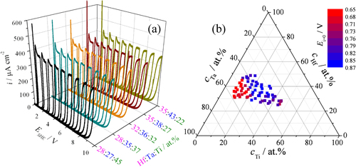
Due to the presence of the natural oxide on the metallic surface before anodization, all the CV plots presented in figure (a) show during the first scan starting from 0 V an initial region when the current is still zero even though the applied potential becomes greater than zero. The potential where the electric field becomes large enough for driving the ion hopping mechanism beyond the volume of the natural oxide (the current onset potential) is termed potential of zero current. This is a material-specific constant directly related to the thickness of the natural oxide for various compositions along the entire Hf–Ta–Ti library.
The potentials of zero current, evaluated from the passive region of the first CV plot recorded, are shown as colour-coded plots in a ternary compositional diagram in part (b) of figure . Low Ti concentrations combined with a minimum of 45 at.% Ta, corresponding to the amorphous composition zone shown in figure , led to smaller passive ranges and consequently thinner natural oxides grown on the surface of the Hf–Ta–Ti library. This is suggested by the red coloured experimental points with values of approximately 0.65 V. With the increase in Ti concentration, the zero current potential values are gradually increased to 0.87 V during the formation of crystalline structures in the alloys. Intermediate values around 0.76 V (violet colour) were measured for Hf concentrations lower than 30 at.%, which correspond to the top line of SEM images from figure in the Ti-rich zone.
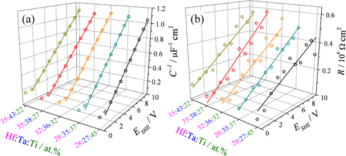
The low and high frequency impedance measurements performed after each step of anodic oxide thickness increase allowed determination of the electrical resistance (R) and capacitance (C) of the oxides. At low frequencies, phase values smaller than −70° were measured while at high frequencies values close to −90° were always found. For each investigated spot on the surface of the Hf–Ta–Ti library, the dependence of the inverse capacitance and resistance of the growing oxide on the anodization potential was investigated. Some of these results are shown for various concentrations in figures (a) and (b). The slopes of the inverse capacitance and resistance curves directly allow the calculation of the dielectric constant and electrical resistivity, respectively. Such curves were automatically recorded for each investigated composition in the Hf–Ta–Ti library.
Figure 4 Inverse capacitance (a) and resistance (b) of mixed anodic oxides grown on Hf–Ta–Ti thin films at various formation potentials.
In order to correlate the oxide formation potentials with the oxide thickness, the oxide formation factors (k) were calculated from the current density plateaus observable in figure (a) and the results are summarized in the ternary compositional map in figure (a). The oxide formation factors of the Hf–Ta–Ti thin films vary between 1.98 and 2.24 nm V−1. Overall, the values increase with increase in Ti concentration in the as-deposited metal alloys and no significant variation was observed within the amorphous compositional zone.
Figure 5 Oxide formation factors (a) and dielectric constants (b) of anodic oxides grown on Hf–Ta–Ti thin films.
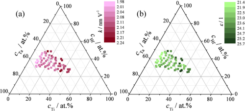
Once the formation potential could be translated into thickness by the k factor, the slopes of the inverse capacitance plots (see figure (a)) can directly deliver the values of the anodic oxide's dielectric constant. These values are mapped in part (b) of figure as a function of the thin film compositions. The variation of the dielectric constant follows a similar trend to the evolution of the oxide formation factors. The increase in Ti concentration produced a small variation of the permittivity from approximately 21 to almost 26.
The slopes of the linear fits of the oxide resistance dependence on the formation potential allow the calculation of the electrical resistivity of the anodic oxides grown on the Hf–Ta–Ti compositional spread. These results are summarized in a colour-coded map, figure (a). The electrical resistivity values show a relatively large scattering in the surface mapping, due to the low current values, or respectively high absolute impedance values measured during the EIS at 0.1 Hz. The anodic oxides’ resistivities ranged approximately between 0.5 × 10¹¹ and 5.0 × 10¹¹ Ω cm. Also in this case, Ti appears to dictate the oxide properties, since the electrical resistivity decreases with the increase of Ti concentration in the as-deposited alloys. This trend can be explained using the individual properties of each oxide, as described by their band gap, since Ta2O5 and Hf2O are insulators while TiO2 shows semiconducting properties [Citation34].
Figure 6 (a) Electric resistivities of anodic oxides grown potentiodynamically on Hf–Ta–Ti alloys. (b) Mott–Schottky plots for anodic oxides potentiostatically grown on Hf–Ta–Ti thin films.

Mott–Schottky analysis was used for assessing the semiconducting properties of the anodic oxides grown on Hf–Ta–Ti thin films by measuring the changes in the capacitance (CSC) as a function of the electrode potential. This capacitance is dominated by the capacitance of the space charge layer in the outer region of the potentiostatically grown oxide. The expression of the Mott–Schottky equation was used:
(1)
where E − EFB represents the potential difference across the oxide film with EFB being the flat band potential, q is the elementary charge, kB is the Boltzmann constant, T is the temperature, ND is the density of the carriers (donors), ε is the dielectric constant of the oxide and ε0 is the vacuum permittivity. Several curves are exemplified in figure (b). Various compositions of the initial metal alloys induced different behaviours of the inverse squared capacitance as function of the applied bias. Semiconducting properties were observed in Mott–Schottky plots measured on oxidized alloys having a high Ti concentration. For Ti concentrations smaller than approximately 20 at.%, which includes the amorphous compositional zone, no evident semiconducting properties were observed. This is seen in the curves corresponding to the lowest Ti amount figure (b). They no longer show a proper behaviour of a semiconducting oxide since the influence of tantalum forming an insulating oxide starts being dominant. In such a case both donor density and flat band potential which would be determined by a formal calculation yield values with high errors. Therefore these values have not been included in further discussions and the Mott–Schottky plots are shown for illustration. For semiconductors in general flatband potential and charge carrier concentration depend on the frequency used for measuring the Mott–Schottky behaviour. Depending on the exact shape of the band structure this frequency can influence both values, but in some cases mainly the charge carrier concentration changes while the flat band remains rather constant. The frequency dependency is stronger for small band gaps. The semiconducting oxides grown on the valve metal library exhibit rather large band gaps resulting in a smaller frequency dependence. This possible influence should be kept in mind since only a single frequency has been used here. For an application in which exactly this physical property is important it would be possible to perform all measurements at different frequencies and limit the compositional range to the region in which the oxides formed are semiconducting. As said before, some oxide show very insulating properties; for these oxides a proper determination is no longer possible and some other methods such as photocurrent spectroscopy must be employed. Such an experimental advancement has been recently implemented as photoelectrochemical SDCM by the authors and will be used in the near future for complementing studies [Citation35].
The linear parts of the Mott–Schottky plots can be used for calculation of the oxides’ flat band potentials (EFB) and donor concentrations (ND) (see equation (Equation1(1) )). In figures (a) and (b) the EFB and ND values are presented which were fitted using the Renka–Cline interpolation method [Citation36]. The Ti concentrations of the as-deposited metal thin films are given in both graphs complementary to the displayed Ta and Hf concentrations. The surface defined by the flat band potential values has a regular shape and EFB continuously decreases with the decrease in Ti concentration in the Hf–Ta–Ti compositional spread. At high Ti concentrations, positive values around 0.1 V versus standard hydrogen electrode (SHE) can be observed which quickly decrease toward −0.8 V SHE once the Ti concentration becomes lower than 35 at.%. The curvature direction of the flat band potential surface is parallel with the direction of the Ti gradient in the alloys, since TiO2 is the only semiconductor possible to form in the anodic oxide, thus affecting its properties. Values determined for high Ta content are not reliable as it was explained before and have therefore not been used in this plot and only shown in figure (b) for illustration purposes.
Figure 7 Surfaces of the flat band potentials (a) and donor density (b) measured on the anodized Hf–Ta–Ti thin films.
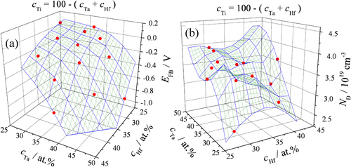
The surface of the donor density plot has an irregular shape with values ranging approximately between 2.5 × 10¹⁹ and 4.0 × 1019 cm−3. Two main curvature directions normal to each other can be identified in figure (b). One of these directions is perpendicular to the direction of the Ti gradient at approximately 30 at.% Ti. This defines the main decrease in the donor density values which follow the combined direction of the Ta decrease and Hf increase gradients in the Hf–Ta–Ti library.
Surface analytical investigations
Surface analytical investigations of the anodic oxides were done by means of qualitative analysis of XPS profiles during depth sputtering. Several XPS spectra measured at three extreme compositions and various sputtered depths are presented in figure for several different compositions of the as-deposited alloys. The depth scale is given in each graph on the right side as calibrated to SiO2. In all investigated cases, TiO2, Ta2O5 and HfO2 were simultaneously present on the surface of the anodized spots suggesting the formation of mixed oxides. All three components of the mixed oxide can be tracked along the sputtering profile. The left column of the graphs in figure shows the Ti spectra while Ta and Hf are displayed together in the right column due to their contiguous binding energy values.
Figure 8 XPS depth profiles of anodic oxides grown at 10 V SHE on Hf–Ta–Ti thin films. BE stands for binding energy.
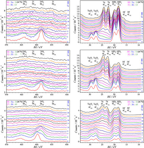
For Ti concentrations of around 13 at.%, TiO2 was present at depths down to 6 nm and no metallic Ti was found. The increase in the Ti content of the thin film to 43 at.% resulted in the presence of TiO2 deeper in the mixed anodic oxides. Both, oxidized and metallic states of Ta and Hf were found in the XPS depth profiles. Higher concentrations of Ta in the alloys resulted in the formation of Ta2O5 at greater depths as shown for the composition containing 55 at.% Ta where the oxide is still present at the maximum probed depth of 30 nm. For all investigated concentrations, metallic Ta can be observed at depths over a few nanometres, suggesting the presence of Ta atoms trapped inside the mixed anodic oxide during its potentiodynamic formation. However this cannot be stated conclusively, due to the Ar sputtering process which can reduce oxidized species to lower oxidation states and even down to their metallic form, thus interfering with the depth profile analysis. For various concentrations of the Hf–Ta–Ti thin films, HfO2 is always present in the entire volume of the mixed oxide. Small peaks corresponding to the metallic Hf were identified at depths as large as 26 nm for the alloys containing 51 at.% Hf.
For a quantitative evaluation of the mixed oxides grown on the surface of the Hf–Ta–Ti thin films, integration of the XPS spectra recorded on the surface of the oxide was performed for several compositions of the metal thin films and the results are summarized in table . In the first two columns, the compositions of the thin films and the mixed oxide compositions are given, respectively. The mixed oxide composition shows deviations from the initial metal composition. These deviations are given in the last three columns in % as related to the values of the metallic thin film compositions.
Table 1. Metal concentration ratios for the as-deposited metal thin films (Me), anodic oxides (Ox) and their individual variations with respect to the metal concentrations (ΔMe;Ox).
Ti shows an enrichment in the oxidized state as compared to its metallic phase and the deviation is affected not only by the Ti concentrations, but also by the Ta and Hf contents. For the same concentration of Ti in the alloys (13 at.%), the deviation of the oxidized Ti amount increases from +56.2 to +73.8% due to the increase of Ta and decrease of Hf concentrations. The two deviations correspond, respectively to Hf-rich and Ta-rich extremes of the amorphous compositional zone (see figure ). In the oxidized form, Ta has a more uniform evolution, with a deficit between 35.1 and 46.9% as compared with the amounts of Ta in the metallic state. The oxide composition shows the minimum deviation for the highest Ta concentration in the alloys of 55 at.%. Hf also shows a slight enrichment in the oxidized state, but the deviations are smaller as compared with Ti and Ta. In the case of the thin film with the highest Ti content (43 at.%) and lowest Hf concentration (27 at.%), the amount of oxidized Hf in the anodic oxide was smaller by almost 3% normalized to the amount of metallic Hf in the initial alloy. Overall, the compositional deviations of the anodic oxides grown on Ti–Ta–Hf thin films have a complex behaviour, which is related to the different individual ionic transport numbers.
Conclusions
In conclusion, a ternary Hf–Ta–Ti thin film combinatorial library deposited by co-sputtering on a Si wafer was analysed by SEM and the microstructure was correlated with the crystallographic properties investigated by XRD. An EDX mapping allowed the identification of all thin film compositions formed in the library. An amorphization zone was identified in a range of the as-deposited metal thin films, coincident with enrichment in Ta. Anodic oxidation of the thin films using the automated SDCM allowed in situ mapping of oxide properties. The specific oxide formation factors corresponding to each oxide were measured as material constants, allowing a direct correlation between the anodization potential and the final oxide thickness. EIS investigations allowed the direct measurement of the dielectric constants and the electrical resistivities of the anodic oxides as a function of the metal concentrations. Mott–Schottky analysis was employed for probing the semiconducting properties of the mixed anodic oxides. Type n semiconductors were identified at high concentrations of Ti and their flat band potentials and donor densities were mapped along the Hf–Ta–Ti compositional spread. XPS depth profiling was used for the qualitative and quantitative evaluation of the mixed anodic oxides. An enrichment of TiO2 simultaneously with a decrease in the Ta2O5 amount on the surface of the mixed oxides was identified as compared with the composition of the metal thin films.
Acknowledgments
Some of the measurements presented here were performed at the Max Planck Institut für Eisenforschung GmbH in Düsseldorf, Germany. The authors acknowledge this instrumental support.
Related Research Data
References
- MusterT HTrinchiAMarkleyT ALauDMartinPBradburyABendavidADligatchS 2011 Electrochim. Acta 56 9679 10.1016/j.electacta.2011.09.003
- Darby MarkS BGuerinSHaydenB ESchreinerH-JYakovlevS 2013 J. Appl. Phys. 113 014104 10.1063/1.4773101
- YoungL 1961 Anodic Oxide Films London Academic
- LohrengelM M 1993 Mater. Sci. Eng. R11 243 10.1016/0927-796X(93)90005-N
- SchultzeJ WHasselA W 2003 Encyclopedia of Electrochemistry vol 4 Weinheim Wiley-VCH
- HasselA WDiesingD 2002 Thin Solid Films 414 296 10.1016/S0040-6090(02)00453-4
- StellaKBuerstelDHasselbrinkEDiesingD 2011 Phys. Status Solidi RRL 5 68 10.1002/pssr.201004510
- OkazakiYNagataH 2012 Sci. Technol. Adv. Mater. 13 064216 10.1088/1468-6996/13/6/064216
- Vivero-EscotoJ LChiangY-DWuK C-WYamauchiY 2012 Sci. Technol. Adv. Mater. 13 013003 10.1088/1468-6996/13/1/013003
- ChoiJ HMaoYChangJ P 2011 Mater. Sci. Eng. R72 97 10.1016/j.mser.2010.12.001
- DurraniS M A 2007 Sensors Actuators B 120 700 10.1016/j.snb.2006.03.034
- GrugerHKunathCKurthESorgeSPufeWPechsteinI 2004 Thin Solid Films 447 509 10.1016/j.tsf.2003.07.013
- LuJKuoYTewgJ Y 2006 J. Electrochem. Soc. 153 G410 10.1149/1.2180647
- LuJKuoY 2005 Appl. Phys. Lett. 87 232906 10.1063/1.2140482
- FangQ 2003 Thin Solid Films 428 263 10.1016/S0040-6090(02)01221-X
- KukliKRitalaMLeskeläMSundqvistJOberbeckLHeitmannJSchröderUAarikJAidlaA 2007 Thin Solid Films 515 6447 10.1016/j.tsf.2006.11.049
- NakajimaMMiuraYFushimiKHabazakiH 2009 Corros. Sci. 51 1534 10.1016/j.corsci.2008.10.021
- HonY HWangJ YPanY N 2004 Mater. Lett. 58 3182 10.1016/j.matlet.2004.06.009
- SeoS MKimI SLeeJ HJoC YMiyaharaHOgiK 2007 Metall. Mater. Trans. A 38 883 10.1007/s11661-007-9090-0
- MardareA ILudwigASavanAWieckA DHasselA W 2010 Electrochim. Acta 55 7884 10.1016/j.electacta.2010.03.066
- MardareA ILudwigASavanAWieckA DHasselA W 2009 Electrochim. Acta 54 5171 10.1016/j.electacta.2009.01.016
- MardareA ISavanALudwigAWieckA DHasselA W 2009 Corros. Sci. 51 1519 10.1016/j.corsci.2008.12.003
- TsuchiyaHAkakiTNakataJTeradaDTsujiNKoizumiYMinaminoYSchmukiPFujimotoS 2009 Corros. Sci. 51 1528 10.1016/j.corsci.2008.11.011
- LudwigAZarnettaRHamannSSavanAThienhausS 2008 Int. J. Mater. Res. 99 1144 10.3139/146.101746
- ThienhausSHamannSLudwigA 2011 Sci. Technol. Adv. Mater. 12 054206 10.1088/1468-6996/12/5/054206
- HasselA WLohrengelM M 1997 Electrochim. Acta 42 3327 10.1016/S0013-4686(97)00184-9
- MardareA IKaltenbrunnerMSariciftciN SBauerSHasselA W 2012 Phys. Status Solidi a 209 813 10.1002/pssa.201100785
- MardareA IWieckA DHasselA W 2007 Electrochim. Acta 52 7865 10.1016/j.electacta.2007.06.048
- MardareA ILudwigASavanAHasselA W 2013 Electrochim. Acta 110 539 10.1016/j.electacta.2013.03.065
- MardareA IYadavA PWieckA DStratmannMHasselA W 2008 Sci. Technol. Adv. Mater. 9 035009 10.1088/1468-6996/9/3/035009
- LillK AHasselA W 2006 J. Solid State Electrochem. 10 941 10.1007/s10008-006-0158-3
- MardareA IHasselA W 2009 Rev. Sci. Instrum. 80 046106 10.1063/1.3117210
- MardareA I 2010 High Throughput Growth of Anodic Oxides on Valve Metals Saarbrücken VDM Verlag Dr Müller p 31
- SchultzeJ WLohrengelM M 2000 Electrochim. Acta 45 2499 10.1016/S0013-4686(00)00347-9
- KollenderJ PMardareA IHasselA W 2013 ChemPhysChem. 14 560 567 560–7 10.1002/cphc.201200656
- RenkaR JClineA K 1984 Rocky Mt J. Math. 14 223 10.1216/RMJ-1984-14-1-223