
Abstract
TiO2 nanorod arrays (TiO2 NRAs) sensitized with CdS nanoparticles were fabricated via successive ion layer adsorption and reaction (SILAR), and TiO2 NRAs were obtained by oxidizing Ti NRAs obtained through oblique angle deposition. The TiO2 NRAs decorated with CdS nanoparticles exhibited excellent photoelectrochemical and photocatalytic properties under visible light, and the one decorated with 20 SILAR cycles CdS nanoparticles shows the best performance. This can be attributed to the enhanced separation of electrons and holes by forming heterojunctions of CdS nanoparticles and TiO2 NRAs. This provides a promising way to fabricate the material for solar energy conversion and wastewater degradation.
1. Introduction
Since the first report of photocatalytic splitting of water using titanium dioxide (TiO2) photoanode by Fujisima and Honda in 1972 [Citation1], TiO2 has been extensively studied and has been considered a superior candidate for solving environmental concerns owing to its low cost, photostability, chemical inertness, nontoxicity, and strong photocatalytic activity [Citation2]. However, the widespread applications of TiO2 are limited due to its large band gap (∼3.2 eV and 3.0 eV for anatase and rutile, respectively), which makes it active only under ultraviolet (UV), i.e. it uses less than ∼5% solar energy) [Citation3]. To enhance the solar energy conversion efficiency of TiO2, one strategy is to extend its photoresponse to visible light, which comprises a greater portion (∼45%) of the solar spectrum [Citation4, Citation5]. This can be achieved by several strategies such as doping with impurities [Citation6–Citation11], coupling with dyes [Citation12–Citation14] and sensitizing with semiconductors [Citation15, Citation16] that have proper conduction band levels. Recently, narrow band gap semiconductors such PbS [Citation17], CdSe [Citation18], ZnS [Citation19] and CdS [Citation20, Citation21] have been successfully studied as sensitizer for TiO2 nanostructures that exhibit obviously enhanced response under visible light. For instance, CdS has a low band gap (∼2.4 eV) and a relatively high absorption coefficient in the visible light region, and its conduction band is more negative than that of TiO2 [Citation22]. The electrons generated in the CdS by the visible light radiation transfer to TiO2 thus separating the photon-induced electrons and holes in the CdS and TiO2, respectively. These properties make CdS highly desirable for use in photoelectrochemisty and photocatalysis in comparion with other semiconductors [Citation23]. CdS nanoparticles (NPs) have several advantages, namely a high extinction coefficient, spectral tunability by size, and good stability. They can be grown directly on TiO2 by electrodeposition [Citation24], chemical bath deposition (CBD) [Citation25], and successive ion layer adsorption and reaction (SILAR) [Citation26, Citation27]. For the SILAR method, the amount of the CdS NPs can be easily controlled by altering the number of deposition cycles. To obtain good electron–hole separation efficiency is crucial for enhancing the photocatalytic [Citation28]. For example, reducing the thickness of the TiO2 could decrease the diffusion pathway of the photo-generated holes to the electrode/electrolyte interface to avoid recombining with photo-generated electrons as TiO2 has a short hole diffusion length (∼10 nm) [Citation29]. Fabricating nanostructures such as nanoparticles, porous nanospheres, nanotubes, nanowires, nanobelts, nanoneedles, and nanorods is a promising way to enhance solar energy conversion efficiency of TiO2, as nanostructures exhibit many desirable characteristics for effective photocatalysis such as efficient and tunable optical absorption, large surface areas, short charge carrier diffusion lengths and low reflectivity [Citation30]. One-dimension (1D) nanostructures such as nanorods can be obtained by organometallic chemical vapor deposition (OMCVD) [Citation31], hydrothermal processes [Citation32], glancing angle deposition (GLAD) [Citation33] and oblique angle deposition (OAD) [Citation34]. The OAD technique is a unique physical vapor deposition process used to fabricate large area, uniform, aligned nanorod arrays with controlled porosity, where the vapor flux is incident onto a substrate at a large angle θ (θ > 70°) with respect to the substrate normal. Due to a geometric shadowing effect, well-aligned and separated nanorod arrays can be produced [Citation35]. The film resulting from the OAD technique presents very open and porous microstructure where nanometer-size columns with a high internal porosity are separated by wide pores that extend from the substrate up to the film surface [Citation36], which is very advantageous in increasing the interface between nanorod and solution. Moreover, the porosity can be readily tuned by varying the oblique angle and various substrates such as glass, F-doped SnO2 (FTO), Si, etc, can be used.
To the aim of improving the TiO2 properties under visible light, fabricating large area uniform TiO2 nanorod arrays (TiO2 NRAs) decorated with CdS NPs is a promising way to harvest solar energy and enhance solar energy conversion efficiency by coupling the traits of TiO2 nanorods and CdS nanoparticles.
In this paper, we obtain TiO2 NRAs by annealing Ti NRAs that are fabricated using the OAD technique, and CdS particles are deposited on TiO2 NRAs by successive ion layer adsorption and reaction (SILAR). The photocatalytic and photoelectrochemical properties of the TiO2 NRAs/CdS film under visible light improve noticeably compared to the bare TiO2 NRAs and CdS films, respectively.
2. Materials and methods
2.1. TiO2 NRAs fabrication
The Ti NRAs were deposited on planar Si substrates and transparent FTO substrates (20 Ω per square) by the oblique angle deposition technique (OAD) described elsewhere [Citation37], and the films deposited on the Si substrates were used for scanning electron microscopy (SEM) and Raman measurements. The substrates were sequentially cleaned in acetone and alcohol by ultrasonic, and then rinsed in deionized water for 5 min each. The system was pumped down to a base pressure of 4 × 10⁻⁸ Torr, and then the Ti film was deposited on the substrate at a deposition rate of 0.5 nm s−1, which was monitored by a quartz crystal microbalance. To produce the films of aligned Ti NRAs, the incident beam of the Ti flux was set at ∼85° with respect to the substrate normal at room temperature. In order to obtain TiO2 NRAs, the Ti NRAs were oxidized in a tube furnace, the furnace was heated up to 450 °C for 2 h at a rate of 5 °C min−1 in ambient atmosphere, resulting in crystalline TiO2 NRAs with good photocatalytic activity.
2.2. CdS NPs deposition on TiO2 NRAs
CdS NPs were deposited on TiO2 NRAs via a successive ionic layer adsorption and reaction (SILAR) method with slight modification, as previously reported [Citation21]. Briefly, the TiO2 NRAs substrates were successively exposed to Cd(Ac)2 and Na2S solutions, respectively, to deposit CdS nanocrystallites. The TiO2 NRAs were immersed in a Cd(Ac)2 (0.05 M) solution for 30 s, and were then rinsed with deionized water and immersed in a solution of Na2S (0.05 M) for another 30 s followed by another rinsing with deionized water. This SILAR process was repeated until the desired deposition of CdS nanocrystallites was achieved.
2.3. Measurements
2.3.1. Experimental setup
The surface morphology was observed by field emission scanning electron microscopy (SEM, JEOL-7001F). A Rigaku 2500 x-ray diffractometer was employed to investigate the crystallographic characteristics of the TiO2 NRAs/CdS NPs. The TiO2 NRAs/CdS NPs were also characterized by transmission electron microscope (TEM, JEOL-2010F). Absorption spectra were recorded using a UV–vis spectrophotometer (PerkinElmer Lambda 950). The Raman and photoluminescence (PL) spectra were recorded using Raman spectrometer (LabRAM ARMIS) under 488 nm and 325 nm excitation, respectively.
2.3.2. Photocatalytic discoloration of methyl orange
Methyl orange (MO) was considered as a model contaminant in the purification of dye wastewater. The prepared samples (15 mm × 15 mm) were placed in a quartz cell containing 10 mL of MO (5 μM) aqueous solution. The photocatalyst was 5 cm away from the quartz window. The relative concentration of MO in the solution was determined by comparing its UV–vis absorption intensity with that of the initial MO solution at 462 nm.
The photocurrent intensity versus potential (I–V curve) measurements were carried out in a 250 mL quartz cell connected to an electrochemistry workstation (CHI 660, Shanghai Chenhua Instrument). A three-electrode assembly was adopted for the test, which included a prepared TiO2 NRAs/CdS NPs as a working electrode, a Pt foil as a counter electrode, a KCl saturated Ag/AgCl as a reference electrode and 0.1 M Na2S as an electrolyte. The working electrode was illuminated with a 300 W Xe lamp. An ultraviolet cutoff filter was inserted between the light source and the quartz cell to exclude UV light with the wavelength shorter than 420 nm. Photocurrent densities were measured in the light on–off process with a pulse of 30 s using the potentiostatic technique [Citation38] under visible light illumination of 130 mW cm−2 and 0 V bias versus Ag/AgCl electrode.
3. Results and discussion
Figure (a) shows a typical top-view SEM image of Ti NRAs prepared by the OAD technique by electron beam evaporation, and the inset shows a typical tilted angle–view SEM image of the NRAs. One sees that the Ti nanorods are 50–90 nm in diameter, ∼220 nm in length, and well separated. Figure (b) shows a typical top-view SEM image of the TiO2 NRAs obtained by oxidizing the Ti NRAs at 450 °C for 2 h in air, and the inset shows a SEM image of the TiO2 NRAs at a tilted angle of 45°. It is seen that the TiO2 nanorods kept the shape and dimensions of Ti nanorods. Figures (c)–(f) show typical top-view SEM images of the TiO2 NRAs after the depositing of CdS NPs by 5, 10, 15, and 20 SILAR cycles deposition, respectively. The SILAR method is an effective way to deposit CdS nanocrystallites on TiO2 nanorods [Citation39, Citation40]. With an increase in the deposition cycle, there are two different types of CdS nanocrystal growth: one is the formation of new crystallites and the other is the growth of smaller crystallites into larger ones [Citation21]. It is seen in figure (e) that after 15 cycles, large CdS crystallites (∼40–50 nm) consisting of several nanocrystallites were deposited on the TiO2 nanorods. After 20 cycles, as shown in figure (f), the CdS nanocrystallites aggregated and formed larger crystallites (∼60–70 nm). It is observed that after CdS deposition by 20 cycles, the decorated TiO2 nanorods are still separated. However, as shown in figure S1, the entire surface of the TiO2 NRAs were covered by a film consisting of larger CdS crystallites, after 25 cycles of deposition.
Figure 1. SEM images of the samples: (a) Ti NRAs; (b) TiO2 NRAs obtained from oxidation of Ti NRAs. The insets in (a) and (b) are the images recorded at a tilt angle of 45°; after (c) 5, (d) 10, (e) 15, and (f) 20 SILAR cycles of CdS deposition.
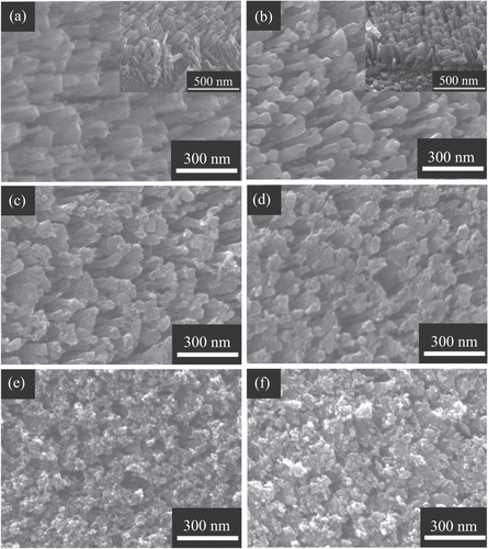
Figure (a) displays the XRD patterns of the TiO2 NRAs deposited with CdS NPs for different SILAR cycles. The diffraction peak at 2θ = 27.3° corresponding to the (110) crystal planes of the rutile phase (JPCDS No. 21-1276) is observed. The presence of a broad XRD peak is an indication of small crystallite size in the nanoscale range, affirming the nanocrystalline nature of the nanorods. To clarify the structure of as-prepared TiO2 NRAs, we measured the as-prepared samples using XRD with the step scanning method. The XRD measurement was performed with a scanning step of 0.01° and with a dwell time of 2 s in the scanning range of 23.5°–28.5°. The corresponding XRD pattern of the as-prepared sample was shown in the inset of figure (a), which displays two distinctive peaks at 25.3° and 27.3°, corresponding to anatase (101) and rutile (110), respectively. In the original XRD patterns measured with the glancing angle x-ray diffraction (GXRD) method, only one broad peak centered at ∼27.3°Can be observed, with which the diffraction peak related to the anatase (101) plane is superimposed.
Figure 2. (a) X-ray diffraction (XRD) patterns of the TiO2 NRAs/CdS NPs. Inset is the XRD pattern of TiO2 NRAs by step scanning method in the scanning range of 23.5°–28.5°; (b) Raman spectrum of TiO2 NRAs. A: anatase, R: rutile, Si: Si substrate.
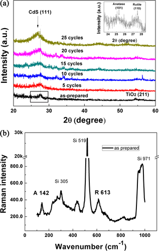
It is noticed that the peak at 2θ = 27.3° shifts to a lower angle gradually with increasing SILAR cycles. After 25 SILAR cycles deposition, a peak at 2θ = 26.5° is formed, indicating a preferred orientation along the (111) plane of the cubic phase CdS (JCPDS No. 89-0440). These result confirm the successful deposition of CdS on TiO2 NRAs.
The Raman spectrum of TiO2 NRAs is shown in figure (b). The anatase and rutile structure belongs to I41/amd space group and P42/mnm tetragonal space group, respectively. The first peak at 144 cm−1 as a characteristic of anatase is formed in the as-prepared TiO2 NRAs. The peak at 613 cm−1 can be assigned to the Raman active modes of the rutile [Citation41, Citation42]. One sees that the TiO2 NRAs consist of a mixture of anatase and rutile nanocrystallites, which will be further verified by TEM.
The growth of CdS NPs on TiO2 NRAs by SILAR was investigated by high-resolution transmission electron microscopy (HRTEM) analysis. Figures (a), (b) show HRTEM images of TiO2 nanorods obtained by oxidizing Ti nanorods. The TiO2 nanorods are polycrystalline, and consist of both the anatase and the rutile phases. The presence of the anatase–rutile heterojunction in the nanorods may help the rutile particles to efficiently collect photon-induced electrons from the anatase particles to reduce the charge recombination [Citation43]. Figures (c), (d) show HRTEM images of TiO2 nanorods decorated with CdS NPs after 15 cycles of SILAR. It is seen clearly that ultrafine CdS particles with a diameter of ∼5 nm were on the nanorod, forming heterojunctions of CdS and TiO2. After 25 SILAR cycles, as shown in figures (e), (f), the TiO2 nanorods are covered by a CdS film consisting of large CdS NPs (∼50 nm). Energy dispersive x-ray spectrum analysis was also carried out for the CdS NPs decorated TiO2 nanorods. The results are shown in figure S2. It shows that the Ti/Cd ratio was ∼1.50 and ∼0.77 in areas marked by the red rectangles in figures (c) and (e), respectively, confirming that more CdS NPs were grown on TiO2 NRAs at a higher number of deposition cycles.
Figure 3. TEM images and HRTEM images: (a), (b) TiO2 NRAs; (c), (d) 15 SILAR cycles TiO2 NRAs/CdS NPs; (e), (f) 25 SILAR cycles TiO2 NRAs/CdS NPs.
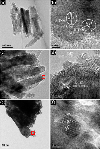
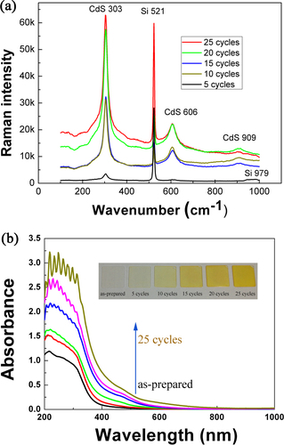
Figure (a) shows the Raman spectra of TiO2 NRAs coated with CdS particles using different numbers of SILAR cycles. One sees that the TiO2 NRAs consist of a mixture of anatase and rutile nanocrystallites, which is in agreement with the HRTEM observation; see figure (b). The three strong Raman peaks located around 303, 606, and 909 cm−1 are assigned, respectively, to the first-, second-, and third-order longitudinal optical (LO) phonon modes of CdS [Citation44, Citation45]. The peaks located at ∼521 and 979 cm−1 are from the silicon substrates [Citation46, Citation47]. The increase in the intensity of the Raman peaks for CdS suggests that more CdS NPs were grown on the TiO2 NRAs, by increasing the SILAR cycles. The optical absorption property of TiO2 NRAs decorated by CdS NPs was measured and is shown in figure (b). The inset of figure (b) is an optical image of the TiO2 NRAs decorated by CdS NPs, showing clearly the color change. The undecorated TiO2 NRAs exhibited absorption in the UV region (at < 380 nm), and a weak absorption in the visible light region which was attributed to the scattering of light caused by pores in the NRAs [Citation38]. Because of the deposition of CdS NPs, all decorated TiO2 NRAs exhibited strong light absorption in a wide region, from 380 nm to 600 nm. In agreement with the color change of the samples (see inset of figure (b)) and Raman analysis (see figure (a)), the absorption capability in the visible light of the CdS-decorated TiO2 NRAs was enhanced monotonically by increasing the SILAR cycles. This may suggest an enhancement in the photocatalytic activity of the decorated TiO2 NRAs in the visible light.
Figure 4. (a) Raman spectra of TiO2 NRAs/CdS NPs; (b) Absorption spectra of the TiO2 NRAs/CdS NPs. Inset is the optical photograph of the TiO2 NRAs/CdS NPs.
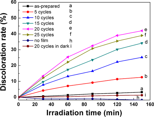
The photocatalytic activity of CdS-decorated TiO2 NRAs was examined by the discoloration of methyl orange upon irradiation with visible light. According to Beer’s law, the intensity of the λ = 462 nm absorbance peak of methyl orange is proportional to the solution concentration, if it is below 0.8 [Citation48]. The discoloration rate η can be calculated by , where Ao and A(t) are the absorbance at 462 nm, at the irradiation time of 0 and t, respectively. Figure plots the discoloration rate of methyl orange as a function of time, using the CdS-decorated TiO2 NRAs as a photocatalyst. One sees that using the undecorated TiO2 NRAs as a photocatalyst, the discoloration rate was only 3.2% even after 150 min of irradiation; this is attributed to the photobleaching process [Citation49]. Enhancement was observed using CdS-decorated TiO2 NRAs as photocatalyst; for example, the discoloration rate was 12.6% when using CdS-decorated TiO2 NRAs by 5 SILAR cycles, and it was 42.0% if using TiO2 NRAs decorated by 20 SILAR cycles. However it is also observed when using the TiO2 NRAs decorated by 25 SILAR cycles as a catalyst, though more CdS NPs were grown (see figures –), and the discoloration rate decreased, i.e. it was down to 39.0%.
Figure 5. Visible light (λ 420 nm) discoloration of MO using TiO2 NRAs/CdS NPs as catalyst.
We have performed photoelectrochemical I–V, photocurrent measurements, and PL measurements to better understand the photocatalytic performance of these TiO2 NRAs decorated by CdS NPs. Figure (a) shows the I–V curves measured for CdS-decorated TiO2 NRAs. It is seen that the open circuit potential (Voc), which corresponds to the difference in the apparent Fermi level between the TiO2 NRAs/CdS NPs and the reference electrode [Citation21], is very dependent on the CdS decoration. It was ∼ −0.42 V for TiO2 NRAs without CdS decoration, and became more negative after decorated with CdS NPs; for instance, it was ∼ −1.14 V when decorated by 5 SILAR cycles, and was ∼ −1.21 V when decorated by 20 SILAR cycles. One may also notice that when decorated by 25 cycles, it became less negative than −1.21 V. Following the literature, the shift of the Fermi level towards the more negative potentials indicates a better charge carrier separation and electron accumulation in semiconductor–semiconductor heterojunctions [Citation21, Citation50–Citation52].
Figure 6. (a) I–V characteristics of the TiO2 NRAs/CdS NPs; (b) current versus time measurements of TiO2 NRAs/CdS NPs under 0 V versus Ag/AgCl bias; (c) PL spectra of TiO2/NRAs CdS NPsexcited by 325 nm.
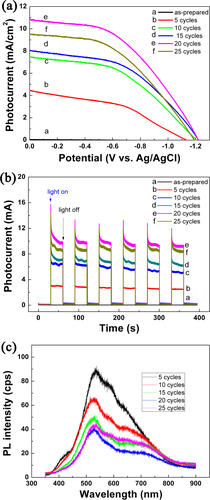
Figure (b) plots the photocurrent of the CdS-decorated TiO2 NRAs versus the incident light irradiation time. It is observed that all the samples exhibited a quick response to the on/off of the incident light, and that the photocurrent was larger for samples decorated by more SILAR cycles. The exception is for the sample decorated by 25 SILAR cycles, which had a smaller photocurrent in comparison with the sample decorated by 20 SILAR cycles. It is well known that a higher photocurrent suggests a higher efficiency in the separation of electrons and holes [Citation53], thus suggesting a better photocatalytic activity. We also fabricated the CdS NPs on bare FTO and Ti NRAs under the same conditions as the CdS NPs deposition on TiO2 NRAs. The photocurrent density versus time coupling irradiation on/off is shown in figure S3. Similar quick responses to the on/off of the incident light are observed in Ti/CdS NPs NRAs due to the properties of CdS NPs; however, the photocurrent density of these is much lower than that of TiO2 NRAs/CdS NPs, indicating the TiO2 NRAs play a role in enhancing the separation efficiency of electrons and holes rather than a temperate.
The PL technique is an effective way to study the efficiency of the charge carrier trapping, migration and transfer, as PL signals result from the recombination of photo-induced carriers. Figure (c) shows the PL spectra of the CdS-decorated TiO2 NRAs. The peaks at ∼425, ∼530 and ∼630 nm can be ascribed to the self-trapped excitons [Citation54] and the oxygen vacancies (Vo) in TiO2 [Citation55, Citation56] and to the sulfur-deficient defects in CdS nanocrystallites [Citation57], respectively. One sees that for samples decorated by more SILAR cycles, the PL intensity was weaker. The exception is for the sample decorated by 25 cycles, which exhibited a stronger PL intensity than the one decorated by 20 cycles. It has been recognized that a lower PL intensity suggests a lower recombination rate of the photo-induced electron–hole pairs [Citation58], and thus a better photocatalytic performance. This is exactly the case we observed here (see figure ).
The optical property of TiO2 NRAs/CdS NPs irradiated with visible light irradiation for 150 min was measured and is shown in figure S4(a). After irradiation, the absorbance of all samples decreases compared to that of the unirradiated sample due to the photo-corrosion in CdS, photo-corrosion occurs when excited electrons and holes are trapped by surface states under visible light irradiation under ambient conditions [Citation59]. To clearly compare the photostability of the TiO2 NRAs/CdS NPs, we depicted the decreasing rate of optical absorbance intensity at 430 nm before and after irradiation as the corrosion rate. It shows clearly that during an exposure time of 150 min, the corrosion rate is more than 30% for the TiO2 NRAs deposited with different SILAR cycles CdS NPs. The photo-corrosion for CdS pollutes the water solution, so it is very necessary to avoid photo-corrosion in future work.
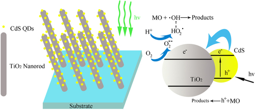
For a semiconductor excited by photons with energies higher than its band gap, electrons are excited from the valence band into the unoccupied conduction band, generating excited electrons in the conduction band and positive holes in the valence band. As shown in figure , when illuminated by visible light, CdS effectively excites electrons and holes. The conduction band of CdS is more positive than that of TiO2 resulting in a local electric field. As a result, the excited electrons can quickly transfer from the CdS to the TiO2 conduction band, whereas the generated holes accumulate in the valence band of CdS to form the holes’ center. Consequently, the excited electron/hole pairs could be separated effectively, which contributed to the improvement of photoelectrochemical properties of TiO2 NRAs/CdS NPs. During the irradiation process, the CdS coupled TiO2 NRAs prolong the lifetime of the photo-induced electrons and holes due to their efficient separation, resulting in an efficient oxidation-reduction reaction, so that the photoactivity can be enhanced. The accumulated electrons in the conduction band of TiO2 can be transferred to oxygen to form active oxygen species (e.g.·O2−), which could be further reduced to highly reactive hydroxyl radicals (OH) [Citation60]. The formed hydroxyl radicals (OH) could further decompose the organic dye MO to intermediates or mineralized products. Furthermore, the holes accumulated in the valence band of CdS could be consumed by participating in a direct reaction with MO molecules to form intermediates or mineralized products [Citation61]. In this study, the discoloration of MO is due to a small part of the photobleaching process, but efficiency depends on the density of the electrons and holes, i.e. the more density, the higher efficiency. Therefore, the photoactivity of TiO2 NRAs/CdS NPs has a positive correlation with the density of the photocurrent, which agrees with the experimental results.
Figure 7. Schematic of light absorption, electrons separation, transfer and degradation of MO process for TiO2 NRAs/CdS NPs.
4. Conclusions
In summary, TiO2 NRAs were fabricated by oxidizing Ti NRAs obtained by oblique angle deposition, CdS NPs deposited on TiO2 NRAs via successive ion layer adsorption and reaction forming heterojunctions of TiO2 NRAs/CdS NPs. The TiO2 NRAs/CdS NPs composites exhibit both excellent visible light photoelectrochemical and photocatalytic properties due to excited electrons injected into TiO2 resulting from the efficient electron–hole separation, and the TiO2 NRAs decorated with 20 SILAR cycles CdS display the best properties. However, aggregate CdS NPs exhibiting a poorer performance were attributed to lower electron–hole separation with increasing the SILAR cycles. Forming heterojunctions of CdS NPs and TiO2 NRAs provides a promising way to fabricate material applied in the solar energy conversion and purification of wastewater.
Acknowledgments
The authors are grateful for the financial support from the National Natural Science Foundation of China (grants 51372135 and 51228101), the financial support from the National Basic Research Program of China (973 program, grant 2013CB934301 and 2010CB731601), the Research Project of Chinese Ministry of Education (grant No. 113007A), and the Tsinghua University Initiative Scientific Research Program.
References
- FujishimaA 1972 Electrochemical photolysis of water at a semiconductor electrode Nature 238 37 38 10.1038/238037a0
- YuanRChenTFeiELinJDingZLongJZhangZFuXLiuPWuL 2011 Surface chlorination of TiO2-based photocatalysts: a way to remarkably improve photocatalytic activity in both UV and visible region ACS Catalysis 1 200 206 10.1021/cs100122v
- BarboriniEContiA MKholmanovIPiseriPPodestàAMilaniPCepekCSakhoOMacovezRSancrottiM 2005 Nanostructured TiO2 films with 2 eV optical gap Adv. Mater. 17 1842 1846 10.1002/adma.200401169
- AbeR 2010 Recent progress on photocatalytic and photoelectrochemical water splitting under visible light irradiation J. Photochem Photobiol. C 11 179 209 10.1016/j.jphotochemrev.2011.02.003
- KudoAMisekiY 2009 Heterogeneous photocatalyst materials for water splitting Chem. Soc. Rev. 38 253 278 10.1039/b800489g
- JagadaleT CTakaleS PSonawaneR SJoshiH MPatilS IKaleB BOgaleS B 2008 N-doped TiO2 nanoparticle based visible light photocatalyst by modified peroxide sol−gel method J. Phys. Chem. C 112 14595 14602 10.1021/jp803567f
- ChenDJiangZGengJWangQYangD 2007 Carbon and nitrogen co-doped TiO2 with enhanced visible-light photocatalytic activity Indust. Eng. Chem. Res. 46 2741 2746 10.1021/ie061491k
- YuJ CHoWYuJYipHWongP KZhaoJ 2005 Efficient visible-light-induced photocatalytic disinfection on sulfur-doped nanocrystalline titania Environ. Sci. Tech. 39 1175 1179 10.1021/es035374h
- ZhouMYuJChengB 2006 Effects of Fe-doping on the photocatalytic activity of mesoporous TiO2 powders prepared by an ultrasonic method J. Hazard Mater. 137 1838 1847 10.1016/j.jhazmat.2006.05.028
- InSOrlovABergRGarcíaFPedrosa-JimenezSTikhovM SWrightD SLambertR M 2007 Effective visible light-activated B-doped and B, N-codoped TiO2 photocatalysts J. Am. Chem. Soc. 129 13790 13791 10.1021/ja0749237
- LiuSGuoEYinL 2012 Tailored visible-light driven anatase TiO2 photocatalysts based on controllable metal ion doping and ordered mesoporous structure J. Mater. Chem. 22 5031 5041 10.1039/c2jm15965a
- ParkYLeeS-HKangS OChoiW 2010 Organic dye-sensitized TiO2 for the redox conversion of water pollutants under visible light Chem. Commun. 46 2477 2479 10.1039/b924829c
- ReisnerEPowellD JCavazzaCFontecilla-CampsJ CArmstrongF A 2009 Visible light-driven H2 production by hydrogenases attached to dye-sensitized TiO2 nanoparticles J. Am. Chem. Soc. 131 18457 18466 10.1021/ja907923r
- KimWTachikawaTMajimaTChoiW 2009 Photocatalysis of dye-zensitized TiO2 nanoparticles with thin overcoat of Al2O3: enhanced activity for H2 production and dechlorination of CCl4 J. Phys. Chem. C 113 10603 10609 10.1021/jp9008114
- LiuBWangDZhangYFanHLinYJiangTXieT 2013 Photoelectrical properties of Ag2S quantum dot-modified TiO2 nanorod arrays and their application for photovoltaic devices Dalton Trans. 42 2232 2237 10.1039/c2dt32031b
- WangMSunLLinZCaiJXieKLinC 2013 p–n heterojunction photoelectrodes composed of Cu2O-loaded TiO2 nanotube arrays with enhanced photoelectrochemical and photoelectrocatalytic activities Energy Environ. Sci. 6 1211 10.1039/c3ee24162a
- LeeHLeventisH CMoonS JChenPItoSHaqueS ATorresTNüeschFGeigerTZakeeruddinS M 2009 PbS and CdS quantum dot–sensitized solid–state solar cells: old concepts, new results Adv. Funct. Mater. 19 2735 2742 10.1002/adfm.200900081
- LeeH JBangJParkJKimSParkS-M 2010 Multilayered semiconductor (CdS/CdSe/ZnS)–sensitized TiO2 mesoporous solar cells: all prepared by successive ionic layer adsorption and reaction processes Chem. Mater. 22 5636 5643 10.1021/cm102024s
- GuijarroNCampiñaJ MShenQToyodaTLana-VillarrealTGómezR 2011 Uncovering the role of the ZnS treatment in the performance of quantum dot sensitized solar cells Phys. Chem. Chem. Phys. 13 12024 12032 10.1039/c1cp20290a
- LiG-SZhangD-QYuJ C 2009 A new visible-light photocatalyst: CdS quantum dots embedded mesoporous TiO2 Environ. Sci. Tech. 43 7079 7085 10.1021/es9011993
- BakerD RKamatP V 2009 Photosensitization of TiO2 nanostructures with CdS quantum dots: particulate versus tubular support architectures Adv. Funct. Mater. 19 805 811 10.1002/adfm.200801173
- DasKDeS 2009 Optical properties of the type-II core–shell TiO2@ CdS nanorods for photovoltaic applications J. Phys. Chem. C 113 3494 3501 10.1021/jp8083953
- LiuYZhouHZhouBLiJChenHWangJBaiJShangguanWCaiW 2011 Highly stable CdS-modified short TiO2 nanotube array electrode for efficient visible-light hydrogen generation Int. J. Hydrogen Energy 36 167 174 10.1016/j.ijhydene.2010.09.089
- WangCSunLYunHLiJLaiYLinC 2009 Sonoelectrochemical synthesis of highly photoelectrochemically active TiO2 nanotubes by incorporating CdS nanoparticles Nanotechnology 20 295601 10.1088/0957-4484/20/29/295601
- LinS-CLeeY-LChangC-HShenY-JYangY-M 2007 Quantum-dot-sensitized solar cells: assembly of CdS-quantum-dots coupling techniques of self-assembled monolayer and chemical bath deposition Appl. Phys. Lett. 90 143517 10.1063/1.2721373
- LuoJMaLHeTNgC FWangSSunHFanH J 2012 TiO2/(CdS, CdSe, CdSeS) nanorod heterostructures and photoelectrochemical properties J. Phys. Chem. C 116 11956 11963 10.1021/jp3031754
- ChengSFuWYangHZhangLMaJZhaoHSunMYangL 2012 Photoelectrochemical performance of multiple semiconductors (CdS/CdSe/ZnS) cosensitized TiO2 photoelectrodes J. Phys. Chem. C 116 2615 2621 10.1021/jp209258r
- ShaislamovUYangB L 2013 CdS-sensitized single-crystalline TiO2 nanorods and polycrystalline nanotubes for solar hydrogen generation J. Mater. Res. 1 1 6 10.1557/jmr.2013.27
- SalvadorP 1984 Hole diffusion length in n-TiO 2 single crystals and sintered electrodes: photoelectrochemical determination and comparative analysis J. Appl. Phys. 55 2977 2985 10.1063/1.333358
- ZhouHQuYZeidTDuanX 2012 Towards highly efficient photocatalysts using semiconductor nanoarchitectures Energy Environ. Sci. 5 6732 6743 10.1039/c2ee03447f
- PradhanS KReucroftP JYangFDozierA 2003 Growth of TiO2 nanorods by metalorganic chemical vapor deposition J. Cryst. Growth 256 83 88 10.1016/S0022-0248(03)01339-3
- NianJ-NTengH 2006 Hydrothermal synthesis of single-crystalline anatase TiO2 nanorods with nanotubes as the precursor J. Phys. Chem. B 110 4193 4198 10.1021/jp0567321
- González-GarcíaLGonzález-VallsILira-CantuMBarrancoAGonzález-ElipeA R 2011 Aligned TiO2 nanocolumnar layers prepared by PVD-GLAD for transparent dye sensitized solar cells Energy Environ. Sci. 4 3426 3435 10.1039/c0ee00489h
- HeYZhangZZhaoY 2008 Optical and photocatalytic properties of oblique angle deposited TiO2 anorod array J. Vac. Sci. Technol. B 26 1350 1358 10.1116/1.2949111
- WolcottASmithW AKuykendallT RZhaoYZhangJ Z 2009 Photoelectrochemical water splitting using dense and aligned TiO2 nanorod arrays Small 5 104 111 10.1002/smll.200800902
- KrauseK MTaschukM THarrisK DRiderD AWakefieldN GSitJ CBuriakJ MThommesMBrettM J 2009 Surface area characterization of obliquely deposited metal oxide nanostructured thin films Langmuir 26 4368 4376 10.1021/la903444e
- XieZZhangYLiuXWangWZhanPLiZZhangZ 2013 Visible light photoelectrochemical properties of N-doped TiO2 nanorod arrays from TiN J. Nanomater. 2013 930950 10.1155/2013/930950
- LiGWuLLiFXuPZhangDLiH 2013 Photoelectrocatalytic degradation of organic pollutants via a CdS quantum dots enhanced TiO2 nanotube array electrode under visible light irradiation Nanoscale 5 2118 2125 10.1039/c3nr34253k
- LeeH JChenPMoonS-JSauvageF D RSivulaKBesshoTGamelinD RComtePZakeeruddinS MSeokS I 2009 Regenerative PbS and CdS quantum dot sensitized solar cells with a cobalt complex as hole mediator Langmuir 25 7602 7608 10.1021/la900247r
- ZewduTCliffordJ NHernándezJ PPalomaresE 2011 Photo-induced charge transfer dynamics in efficient TiO2/CdS/CdSe sensitized solar cells Energy Environ. Sci. 4 4633 4638 10.1039/c1ee02088a
- MaH LYangJ YDaiYZhangY BLuBMaG H 2007 Raman study of phase transformation of TiO2 rutile single crystal irradiated by infrared femtosecond laser Appl. Surf. Sci. 253 7497 7500 10.1016/j.apsusc.2007.03.047
- MaliS SDesaiS KDalaviD SBettyC ABhosaleP NPatilP S 2011 CdS-sensitized TiO2 nanocorals: hydrothermal synthesis, characterization, application Photochem. Photobiol. Sci. 10 1652 1658 10.1039/c1pp05084b
- SunPZhangXWangCWeiYWangLLiuY 2013 Rutile TiO2 nanowire array infiltrated with anatase nanoparticles as photoanode for dye-sensitized solar cells: enhanced cell performance via the rutile–anatase heterojunction J. Mater. Chem. A 1 3309 3314 10.1039/c2ta01432g
- MaliSDesaiSDalaviDBettyCBhosalePPatilP 2011 CdS-sensitized TiO2 nanocorals: hydrothermal synthesis, characterization, application Photochem. Photobiol. Sci. 10 1652 1658 10.1039/c1pp05084b
- WangZGongJDuanJHuangHYangSZhaoXZhangRDuY 2006 Direct synthesis and characterization of CdS nanobelts Appl. Phys. Lett. 89 033102 033103 10.1063/1.2222237
- DaiCChuuDHsiehW 1991 Raman intensity enhancement of the Si peak by CdS thin films Appl. Phys. Lett. 59 3273 3275 10.1063/1.105728
- BalevaMZlatevaGAtanassovAAbrashevMGoranovaE 2005 Resonant Raman scattering in ion-beam-synthesized Mg_ {2} Si in a silicon matrix Phys. Rev. B 72 115330 10.1103/PhysRevB.72.115330
- LiZZhuYZhouQNiJZhangZ 2012 Photocatalytic properties of TiO2 thin films obtained by glancing angle deposition Appl. Surf. Sci. 258 2766 2770 10.1016/j.apsusc.2011.10.129
- ChengPDengCGuMShangguanW 2007 Visible-light responsive zinc ferrite doped titania photocatalyst for methyl orange degradation J. Mater. Sci. 42 9239 9244 10.1007/s10853-007-1902-5
- SubramanianVWolfE EKamatP V 2003 Green emission to probe photoinduced charging events in ZnO-Au nanoparticles. Charge distribution and fermi-level equilibration J. Phys. Chem. B 107 7479 7485 10.1021/jp0275037
- JakobMLevanonHKamatP V 2003 Charge distribution between UV-irradiated TiO2 and gold nanoparticles: determination of shift in the Fermi level Nano Lett. 3 353 358 10.1021/nl0340071
- WoodAGiersigMMulvaneyP 2001 Fermi level equilibration in quantum dot-metal nanojunctions J. Phy. Chem. B 105 8810 8815 10.1021/jp011576t
- LiuYXieCLiJZouTZengD 2012 New insights into the relationship between photocatalytic activity and photocurrent of TiO2/WO3 nanocomposite Appl. Catal. A 433-434 81 87 10.1016/j.apcata.2012.05.001
- LeiYZhangLMengGLiGZhangXLiangCChenWWangS 2001 Preparation and photoluminescence of highly ordered TiO nanowire arrays Appl. Phys. Lett. 78 1125 10.1063/1.1350959
- SantaraBGiriPImakitaKFujiiM 2013 Evidence of oxygen vacancy induced room temperature ferromagnetism in solvothermally synthesized undoped TiO2 nanoribbons Nanoscale 5 5476 88 10.1039/c3nr00799e
- ShiJChenJFengZChenTLianYWangXLiC 2007 Photoluminescence characteristics of TiO2 and their relationship to the photoassisted reaction of water/methanol mixture The J. Phys. Chem. C 111 693 699 10.1021/jp065744z
- YangYChenHMeiYChenJWuXBaoX 2002 CdS nanocrystallites prepared by chemical and physical templates Acta Mater. 50 5085 5090 10.1016/s1359-6454(02)00363-4
- LiqiangJYichunQBaiqiWShudanLBaojiangJLibinYWeiFHonggangFJiazhongS 2006 Review of photoluminescence performance of nano-sized semiconductor materials and its relationships with photocatalytic activity Sol. Energy Mater. C 90 1773 1787 10.1016/j.solmat.2005.11.007
- XuLWangLHuangXZhuJChenHChenK 2000 Surface passivation and enhanced quantum-size effect and photo stability of coated CdSe/CdS nanocrystals Physica E 8 129 133 10.1016/S1386-9477(00)00129-6
- JinSLiYXieHChenXTianTZhaoX 2012 Highly selective photocatalytic and sensing properties of 2D-ordered dome films of nano titania and nano Ag2+ doped titan J. Mater. Chem. 22 1469 1476 10.1039/c1jm14216j
- XieYAliGYooS HChoS O 2010 Sonication-assisted synthesis of CdS quantum-dot-sensitized TiO2 nanotube arrays with enhanced photoelectrochemical and photocatalytic activity ACS Appl. Mater. Interfaces 2 2910 2914 10.1021/am100605a