
Abstract
The efficiency of perovskite solar cells (PSCs) has been improved from 9.7 to 19.3%, with the highest value of 20.1% achieved in 2014. Such a high photovoltaic performance can be attributed to optically high absorption characteristics and balanced charge transport properties with long diffusion lengths of the hybrid lead halide perovskite materials. In this review, some fundamental details of hybrid lead iodide perovskite materials, various fabrication techniques and device structures are described, aiming for a better understanding of these materials and thus highly efficient PSC devices. In addition, some advantages and open issues are discussed here to outline the prospects and challenges of using perovskites in commercial photovoltaic devices.
1. Introduction
Solar energy is the most abundant energy resource on Earth, where every minute enough sunlight reaches the Earth’s surface to meet the world’s energy demands for one year. Currently the conversion of sunlight into energy can be achieved through solar photovoltaic (PV) cells, concentrated PVs and solar thermal technologies. Today, solar energy provides only a small fraction of total global electricity generation (∼1%) but the use of solar PVs is expanding rapidly due to the annual decrease in the cost of such technologies [Citation1]. Solar cells made of crystalline silicon are often referred as first generation solar cells and have dominated the PV market over the past half century [Citation2, Citation3]. ‘Third generation’ PV technologies have been developed to pursue high power conversion efficiency (PCE) and low cost, these include light-condensed cells, organic PVs (OPVs), dye-sensitized solar cells (DSSCs), organic–inorganic hybrid solar cells, and so on. The large flexibility in the shape, color and transparency of third generation solar cells, particularly DSSCs, makes them one of the most promising technologies for photo-to-electricity conversion applications [Citation4–Citation8]. Currently, in the laboratory, DSSCs have reached 13% efficiency under standard reporting conditions [Citation9], providing a credible alternative to the conventional p–n junction PV devices. The major disadvantage in DSSC design is the use of a liquid electrolyte, which suffers from temperature stability problems. Replacing the liquid electrolyte with a solid one is a major, ongoing field of research. Not only the stability, but also the open circuit voltage of a DSSC could be expected to improve when a solid-state hole transfer material (HTM) is used. Thus far, 2, 2’,7,7’-tetrakis(N,N-di-p-methoxyphenylamine)-9,9’-spirobifluorene (spiro-OMeTAD) and its derivatives have been the most popular HTMs in solid-state DSSCs [Citation10–Citation12]. They were first introduced by Bach et al in 1998 [Citation13]. However, a satisfactory PV performance for solid-state cells containing such materials can only be achieved with thin mesoporous photoanodes because of the difficulty of infiltration of HTMs [Citation14, Citation15]. Thus, only light absorbers with high extinction coefficients or a wide absorption spectrum are able to provide sufficient sunlight harvesting in thin films [Citation16–Citation18].
Hybrid lead iodide perovskite materials exhibit a high absorption coefficient up to 1.5 × 104 cm−1 at 550 nm, estimated from a CH3NH3PbI3 coated nanocrystalline TiO2 thin film, which indicates that the penetration depth for 550 nm light is only 0.66 μm [Citation19]. In 2009, Kojima et al reported the first study of the organic lead halide compounds CH3NH3PbBr3 and CH3NH3PbI3 as sensitizers in photo-electrochemical cells [Citation20]. They measured a moderate PCE of 3.81% for the CH3NH3PbBr3-based device and 3.13% for the CH3NH3PbBr3-based device. The stability of these devices was poor in a liquid electrolyte cell configuration. However, the high absorption coefficient makes them one of the best choices for solid-state solar cells. In mid-2012, solid-state DSSCs based on CH3NH3PbI3 demonstrated a PCE of 9.7%, in which spiro-OMeTAD was used as the HTM [Citation21]. The devices exhibited a large photocurrent (JSC) enhancement exceeding 17 mA cm−2, which was superior to the best conventional solid-state DSSCs with organic light-harvesting materials. The use of a solid-state HTM dramatically improved the device’s stability compared to CH3NH3PbI3-sensitized liquid junction cells, although this remains the main issue in the development of perovskite solar cell (PSC). Since then, the PCEs of PSCs have experienced a burst of development. It is worth mentioning that a new method for the fabrication of CH3NH3PbI3-based PSCs with 15.0% efficiency was introduced by Burschka et al, in which the PSCs are sequentially deposited from separate solutions of CH3NH3I and PbI2 [Citation22]. Planar junction PSCs have also been developed by Liu et al and high efficiency devices have been achieved using a dual-source vapor deposition (DSVD) method [Citation23]. Very recently, a certified PCE record of ∼20.1% was attained through interfacial modification of the perovskite layer and electrodes as well as film preparation [Citation24].
PSCs can adopt the merits of inorganic materials, such as stability, high carrier mobility and a compatible fabricating process, and utilize the advantages of organics, such as tunable light absorption, adjustable molecular structures for energy band alignment and facile solution processability. This review descibes the basic characteristics of hybrid lead iodide perovskite materials, various fabrication techniques and device structures to provide better understanding and insight into high-performing PSCs. In addition, the most notable problems and recent progress in research are highlighted with regard to further improvement of PSCs.
2. The basics of hybrid lead halide perovskites
Perovskite is the name of a crystal structure, first found in the inorganic mineral CaTiO3 (ABX3), with a cubic unit cell. In the unit cell, the A-cation resides at the eight corners of the cube surrounded by twelve X-anions, while the B-cation is located at the body center which is surrounded by six X-anions (located at the face centers) in an octahedral [BX6]4− cluster [Citation20, Citation25]. The A and B sites can accommodate inorganic cations of various valences and ionic radii. Alternatively, small organic cations such as CH3NH3+, C2H5NH3+ and HC(NH2)2+ can be used to replace inorganic cation A and create organic–inorganic hybrid materials [Citation26, Citation27]. The metal cations (B) are typically divalent metal ions such as Pb2+, Sn2+ or Cu2+, and the X anions are halides (Cl−, Br−, I−) [Citation25, Citation28–Citation30].
Weber reported the replacement of A by methylammonium cations (MA=CH3NH3+) to generate the first three-dimensional organic–inorganic hybrid perovskites [Citation31, Citation32]. figure (a) shows the general structure of these organometal halide CH3NH3BX3 (B=Pb or Sn, X=Cl, Br or I) materials. Methylammonium lead iodide, CH3NH3PbI3, has interesting optical and electronic properties that have been actively investigated during the past two decades [Citation33, Citation34]. CH3NH3PbI3 is a semi-conducting pigment with a direct bandgap of 1.55 eV corresponding to an absorption onset of 800 nm, which makes this material a good light absorber over the whole visible solar emission spectrum [Citation25, Citation33]. The photon-generated excitons in CH3NH3PbI3 have a weak binding energy of less than 50 meV [Citation35, Citation36], which means that most of them can be dissociated very rapidly into free carriers at room temperature [Citation37]. The electrons and holes produced in this material exhibit small effective masses resulting in high carrier mobilities ranging from 24 ± 7 cm2 V−1 s−1 for electrons to 105 ± 35 cm2 V−1 s−1 for holes [Citation38]. Their recombination occurs on a timescale of hundreds of nanoseconds, resulting in long carrier-diffusion lengths—that is, the average distance that can be covered by carriers before they recombine—ranging between 100 nm and 1000 nm (recently, electron–hole diffusion lengths of >175 μm in MAPbI3 single crystals have also been reported) [Citation38–Citation40]. Even though these appealing properties had already been known for more than 20 years, the extraordinary potential of hybrid perovskites in PV applications was only revealed five years ago [Citation19, Citation20].
Figure 1. Crystal structure of MABX3 (a) and powder XRD pattern (b) (peaks at 2θ angles of 14.1, 28.4 and 43.1 for MAPbI3) of Pb-based halide perovskite materials. The metal cation (B, grey sphere) is located at the body center of the cubic composed of six halide X-anions (purple). The orange sphere represents the CH3NH3+ ion (MA cation). The XRD values are taken from [Citation54] and [Citation41].
![Figure 1. Crystal structure of MABX3 (a) and powder XRD pattern (b) (peaks at 2θ angles of 14.1, 28.4 and 43.1 for MAPbI3) of Pb-based halide perovskite materials. The metal cation (B, grey sphere) is located at the body center of the cubic composed of six halide X-anions (purple). The orange sphere represents the CH3NH3+ ion (MA cation). The XRD values are taken from [Citation54] and [Citation41].](/cms/asset/3f0263fc-1ddd-4951-88b2-827f3d7bdeb0/tsta_a_11661310_f0001_oc.jpg)
Iodine can be partially or entirely replaced by other halogens (Br and Cl) to form different perovskite materials, among which CH3NH3PbBr3 and CH3NH3PbI3−xClx have attracted intense attention. X-ray diffraction (XRD) patterns of these Pb-based halide perovskite materials are shown in figure (b). We note that it is not certain whether the chemical formula of CH3NH3PbI3−xClx is suitable or not, as the role of chlorine in these materials is still under debate. Interestingly, the hybrid lead halide perovskite incorporates two halides (e.g., iodide with bromide), allowing the continuous tuning of the optical bandgap to cover the most visible spectrum (figures (a)–(c)). The introduction of Br elevates the conduction band (CB) and lowers the valence band (VB) for CH3NH3PbBr3, whose direct bandgap is ∼2.2 eV (figure ) [Citation43–Citation46]. Raising the CB minimum is favorable for energy band matching between TiO2 and CH3NH3PbBr3; it suppresses geminate recombination, which results in an improvement of the open-circuit voltage (VOC). Unfortunately, the large bandgap of CH3NH3PbBr3 limits light absorption with an onset wavelength less than ∼550 nm, which would subsequently greatly cut down the photocurrent. Photon-generated excitons of CH3NH3PbBr3 have a higher binding energy of about 150 meV compared to CH3NH3PbI3 (≤50 meV) [Citation36, Citation44]. Therefore, the PCE of PSCs using CH3NH3PbBr3 is still lower than that of CH3NH3PbI3. By partially substituting Pb with Sn one can continuously tune the optical bandgap [Citation47]. The reported threshold of the incident photon to current efficiency of their devices was extended to 1060 nm (figures (d) and (e)).
Figure 2. Photographs and UV–vis absorption spectra of MAPb(I1−xBrx)3. (a) UV–vis absorption spectra of mp-TiO2/MAPb(I1−xBrx)3 films measured using an integrating sphere. (b) Photographs of three-dimensional TiO2/MAPb(I1−xBrx)3 bilayer nanocomposites on a FTO glass substrates. (c) A quadratic relationship of the bandgaps of MAPb(I1−xBrx)3 as a function of Br composition (x). Reprinted with permission from [Citation42]. Copyright 2013 American Chemical Society. (d) Electronic absorption spectra of MASnxPb(1−x)I3 perovskite coated on porous TiO2 with (e) corresponding incident photon-to-current conversion efficiency curves for MASnxPb(1−x)I3 perovskite/poly(3-hexylthiophene) solar cells. Reprinted with permission from [Citation47]. Copyright 2014 American Chemical Society.
![Figure 2. Photographs and UV–vis absorption spectra of MAPb(I1−xBrx)3. (a) UV–vis absorption spectra of mp-TiO2/MAPb(I1−xBrx)3 films measured using an integrating sphere. (b) Photographs of three-dimensional TiO2/MAPb(I1−xBrx)3 bilayer nanocomposites on a FTO glass substrates. (c) A quadratic relationship of the bandgaps of MAPb(I1−xBrx)3 as a function of Br composition (x). Reprinted with permission from [Citation42]. Copyright 2013 American Chemical Society. (d) Electronic absorption spectra of MASnxPb(1−x)I3 perovskite coated on porous TiO2 with (e) corresponding incident photon-to-current conversion efficiency curves for MASnxPb(1−x)I3 perovskite/poly(3-hexylthiophene) solar cells. Reprinted with permission from [Citation47]. Copyright 2014 American Chemical Society.](/cms/asset/c70408b7-c8ee-45c6-9e52-3d3593a62a2e/tsta_a_11661310_f0002_oc.jpg)
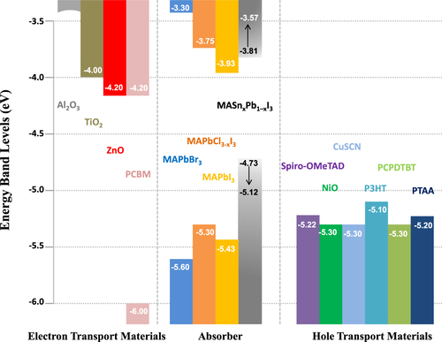
Figure 3. Energy level diagram of the materials used in PSCs.
Different to Br, the introduction of Cl was believed to elevate the formation of perovskite grains by decreasing the surface or bulk defects [Citation25, Citation46]. This enhanced crystallinity can accelerate the transfer and diffusion of photon-generated carriers, thus increasing the electron–hole diffusion lengths. It was reported that the diffusion length of CH3NH3PbI3−xClx exceeds 1 μm, which is far longer than that for CH3NH3PbI3 (∼100 nm) [Citation40].
Regarding the optoelectronic properties of hybrid lead halide perovskite materials, the presence of defect sites in these materials has thus far been ignored, in contrast to c-Si and other crystalline semiconductors, where minimizing impurities and crystal imperfections is critical to prepare the highest efficiency PV cells [Citation48, Citation49]. A high density of point defects (i.e., Schottky defects and Frenkel defects) was created while tuning the ratio of CH3NH3I and PbX sources during the synthesis procedure. Their properties directly determine the charge carrier diffusion length. However, the calculation of the Schottky defects [Citation50] such as PbI2 and CH3NH3I vacancies shows no formation of gap states within the bandgap [Citation51]. These results indicate that point defects in the bulk do not act as charge recombination centers. It was further discovered that the formation energy for deep defects (iodine interstitial in β-CH3NH3PbI3, tetragonal room-temperature phase) can be further increased by Cl doping [Citation52].
3. Perovskite solar cell device structure
During 2014 there were several demonstrations of cells with efficiencies >16% [Citation53, Citation54], along with predictions of a ‘straightforward path to well above 20%’. A range of device strategies yielding high efficiencies has been reported: the regular [Citation22] and inverted electrical geometries [Citation55], with [Citation56, Citation57] or without mesoporous oxide supports [Citation23, Citation55] and using a variety of transport materials (depicted in figure ) [Citation53, Citation58–Citation61]. Device performance with various PSC structures is summarized in table . Figure shows the schematic structures and energetics of two typical devices: mesoscopic nano-structured and planar structured PSC devices. Charge separation by electron injection from the perovskite to the TiO2 is obvious in cases where perovskite dots are adsorbed onto the TiO2 surface. [Citation21] In this case, the working principle is expected to be similar to DSSCs. However, Lee et al reported a PSC comprised of mesoporous Al2O3 instead of TiO2 [Citation65], demonstrating that the Al2O3 merely acted as a scaffold layer without injection of photo-excited electrons. Photo-induced absorption spectroscopy measurements revealed that hole transfer was highly effective from the photo-excited perovskite to the spiro-OMeTAD, generating long-lived charge species within the perovskite layer coated on the Al2O3 nanoparticles. Furthermore, small-perturbation transient photocurrent decay measurements revealed that charge collection was ten times faster in the Al2O3-based cell than in the TiO2-based one, indicating much faster electron diffusion through the perovskite phase than in the n-type TiO2. Sum and Snaith further investigated the balanced long-range electron–hole diffusion properties of organometallic perovskite materials [Citation39, Citation40]. The electron and hole diffusion lengths were estimated to be ∼130 nm and ∼100 nm, respectively, for samples prepared from a CH3NH3I + PbI2 mixture, while longer diffusion lengths of ∼1069 nm for electrons and ∼1213 nm for holes were measured for samples prepared using a 3CH3NH3I + PbCl2 mixture. Subsequent work using iodide prepared by the vapor-phase CH3NH3I conversion of PbI2 resulted in good carrier collection in 350 nm thick iodide films, suggesting that the diffusion lengths exceed this thickness [Citation66]. This is supported by recent electron-beam measurements [Citation67]. Electron beam-induced current (EBIC) imaging studies of CH3NH3PbI3 layers prepared from PbI2 and PbCl2 sources revealed that the charge diffusion lengths were about 1 μm for both samples, in which the diffusion length for holes was longer than that for electrons for the case of CH3NH3PbI3 prepared without a chloride source.
Table 1. Compilation of high efficiency PSCs. States: c = compact, mp = mesoporous and MA=CH3NH3.
Figure 4. The structure of PSCs. (a) The model structure of mesoporous halide PSCs and (b) the model structure of planar heterojunction-structure halide PSCs.
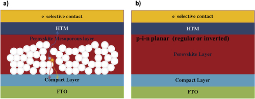
Due to the long carrier lifetime and long diffusion length, bulk organometallic perovskite can also work efficiently without a mesoporous oxide layer or scaffold layer. Perovskite was deposited directly between two thin selective compact layers to construct planar heterojunction-structure halide PSCs. The efficiency of planar PSCs was increased up to ∼19.3% [Citation54]. Carrier transport and recombination were compared for the mesoscopic structure and the planar structure. It was shown that the former was less efficient than the latter, this being the main factor affecting the device’s PV performance [Citation68]. The results showed that the transport rate was the same but the recombination rate was higher for the mesoscopic structure. Recently, Edri et al addressed the fundamental issue of how these planar PSCs work by applying a scanning electron microscopy-based technique to cell cross-sections [Citation69]. By mapping the variation in efficiency of charge separation and collection in the cross-sections, they showed the presence of two prime high efficiency locations: one at/near the absorber/hole-blocking-layer and the second at/near the absorber/electron-blocking-layer interfaces, with the former more pronounced (ss shown in figure ). This ‘twin-peaks’ profile is characteristic of a p–i–n solar cell, with a layer of high electronic quality and low-doped semiconductor (intrinsic perovskite), between a p- and an n-layer. A question arises: how are free carriers generated in this system? Some scientists have suggested that, similarly to organic solar cells, PSCs can be considered as excitonic solar cells, which require a heterojunction interface to separate the photo-generated electron–hole pair. Some have suggested that, similarly to inorganic solar cells, the photo-excitations of perovskites spontaneously dissociate into free carriers in the bulk of the junction. Several reports have revealed a low binding energy for the exciton in perovskites (less than 50 meV) [Citation35, Citation36]. The ultrafast interfacial charge-transfer dynamics [Citation70] in combination with the observation of long electron- and hole-diffusion lengths points at PSCs being predominantly non-excitonic solar cells.
Figure 5. (a) Schematic of an EBIC experiment. A scanned electron beam generates a cloud of carriers, creating a position-dependent current in a short-circuiting load. Reprinted with permission from [Citation67]. Copyright 2014 American Chemical Society. (b) A schematic band diagram of CH3NH3PbI3−xClx perovskite-based cells under light in a p–i–n device structure. The diagram is not to scale and shows only the relative positions of the energy bands. The green dashed lines show the relative quasi-Fermi level.
![Figure 5. (a) Schematic of an EBIC experiment. A scanned electron beam generates a cloud of carriers, creating a position-dependent current in a short-circuiting load. Reprinted with permission from [Citation67]. Copyright 2014 American Chemical Society. (b) A schematic band diagram of CH3NH3PbI3−xClx perovskite-based cells under light in a p–i–n device structure. The diagram is not to scale and shows only the relative positions of the energy bands. The green dashed lines show the relative quasi-Fermi level.](/cms/asset/0e5d92f2-cfdd-40e0-a085-5d59e2eb0010/tsta_a_11661310_f0005_oc.jpg)
Alongside the above discussion, HTM-free PSCs have been under intense investigation. Etgar et al first reported on a hole-conductor-free CH3NH3PbI3/TiO2 heterojunction solar cell [Citation71]. A thick perovskite film with large crystals, which function as light harvesters and hole transport materials at the same time, was deposited on top of mesoporous TiO2. In this case, a thick perovskite layer with a smooth surface is needed to avoid forming shunt pathways as well as to form good back contact to achieve high efficiency. The PV performance of the HTM-free PSC was dependent on the depletion layer width at the TiO2–CH3NH3PbI3 junction. This width can be enlarged by increasing the depleted fraction of TiO2, leading to a PCE of 10.85% [Citation72]. A carbon counter-electrode used in a HTM-free PSC, collocated with a double layer of mesoporous TiO2 and ZrO2 as a scaffold, has been exploited by Mei et al [Citation73]. The ZrO2 layer was found to block the flow of photogenerated electrons to the back contact, retarding recombination with the holes from the perovskite at the back contact. The cell achieved a certified PCE of 12.8%.
4. Progress in perovskite solar cell device performance
The first report of a solid-state PSC device was published in 2012 [Citation21], in which CH3NH3PbI3 was deposited into a 0.6 μm mesoscopic TiO2 film, covered with a hole-conductor spiro-OMeTAD. The device exhibited a large JSC exceeding 17 mA cm–2, a VOC of 0.888 V and a fill factor (FF) of 0.62, yielding a PCE of 9.7% under standard AM 1.5 sunlight. The use of spiro-OMeTAD dramatically improved the device’s stability compared to liquid junction cells in ex situ long-term stability tests conducted for over 500 h, where the devices were stored in air at room temperature without encapsulation. Subsequenty, this group has rarely reported the results of long-term stable PSC devices. After systematic optimization by modifying the conditions for the PbI2 precursor deposition and the transformation reaction, in 2013 Burschka et al reported PSC devices with PCEs up to 15% with JSC, VOC and FF values of 20.0 mA cm−2, 993 mV and 0.73, respectively [Citation22]. Snaith and co-workers used a mixed halide system-CH3NH3PbI3−xClx on both the TiO2 and Al2O3 mesoporous layers [Citation65]. The highest efficiencies (PCE = 10.9%, JSC = 17.8 mA cm–2, VOC = 0.98 V and FF = 0.63) were obtained for the mesoporous Al2O3 devices where they acted purely as scaffolds and did not take part in the electrical processes. A much simpler approach involved the vapor deposition of perovskite films onto TiO2 films which yielded a short-circuit photocurrent of 21.5 mA cm−2, a VOC of 1.07 V, a FF of 0.68 and an efficiency of 15.4% [Citation23]. These concurrent reports sparked an explosion of research activity in which a variety of device configurations, deposition protocols and material sets have been employed. To establish systematic design rules to achieve high efficiencies in simple PSCs, we provide a review of deposition methods and device configuration optimization evolution routes in the following sections.
4.1. Preparation methods for highly efficient devices
4.1.1. Solution process fabrication
To deposit CH3NH3PbI3 onto substrates, two methods have been developed, i.e., the so-called one-step or two-step coating methods (figures (a) and (b)). Perovskite thin film can be formed either by spin-coating a mixed CH3NH3I and PbI2 solution (one-step coating) or by spin-coating PbI2 followed by deposition of CH3NH3I (two-step coating). One-step precursor solution deposition represents the most popular thin film deposition method for PSCs due to its simplicity. Generally, the precursor solution is prepared by mixing powders of MAX (X: I, Br, Cl) and PbX2 (X: I, Br, Cl) at a 1:1 (stoichiometry) or 3:1 (non-stoichiometry) mole ratio in a polar aprotic solvent, such as N, N-dimethylformamide (DMF), gamma-butyrolactone (GBL), or dimethyl sulfoxide (DMSO). However, forming a homogeneous pin-hole-free perovskite layer is still a challenge for the one-step coating process. A poor coverage of the perovskite layer results in poor light absorption as well as a shunting path for charge recombination, which would greatly reduce the device’s efficiency [Citation25, Citation60, Citation65]. Unlike polymeric films, which are mostly amorphous when deposited using the spin-coating technique, it is difficult to control the perovskite crystalline formation. Even a mild temperature heating treatment to remove solvent residues can result in dewetting and roughening of the as-deposited perovskite films [Citation74].
Figure 6. Four general methods for preparing perovskite active layers. (a) One-step precursor deposition, (b) two-step sequential deposition method, (c) DSVD and (d) VASP. Reprinted with permission from [Citation66]. Copyright 2014 American Chemical Society.
![Figure 6. Four general methods for preparing perovskite active layers. (a) One-step precursor deposition, (b) two-step sequential deposition method, (c) DSVD and (d) VASP. Reprinted with permission from [Citation66]. Copyright 2014 American Chemical Society.](/cms/asset/fab008b0-8e67-428f-8d8b-641f2a11d7db/tsta_a_11661310_f0006_oc.jpg)
By including additives in the precursor, a perovskite film with a smooth surface and uniform crystal domains can be formed as a compact layer for planar PSC devices. To improve the solubility of choline and the uniformity of the perovskite crystal layer, CH3NH3Cl [Citation75], 1, 8-diiodooctane [Citation76] or NH4Cl [Citation77] have been added, resulting in PCEs of 12%, 11.8% and 9.93%, respectively. In addition, solvent engineering processes have been intensely investigated. A higher PCE was obtained when a mixture of DMF and GBL (97:3 in volume) was applied, compared with using GBL and DMF alone [Citation78]. As an intermediate phase (CH3NH3I–PbI2–DMSO) was found when a mixture solvent of GBL and DMSO (7:3 in volume) was applied, the DMSO competed with CH3NH3I to retard the crystallization of perovskite [Citation79]. After adding toluene to the solution drop-wise to remove the excess DMSO, a uniform intermediate layer was formed on the m-TiO2 and a certified PCE of 16.2% was achieved. Simultaneously, Xiao et al reported a similar study, in which immediately after spin-coating a CH3NH3PbI3 precursor DMF solution, chlorobenzene was added to induce the fast crystallization of perovskite [Citation80]. A uniform CH3NH3PbI3 layer was formed, yielding an average PCE of 13.9 ± 0.7% on a compact TiO2 substrate. Likewise, the effects of post-annealing processes on perovskite film coverage and optoelectronic properties has also been characterized [Citation54, Citation81, Citation82].
A significant development for solution-based deposition has been the application of the two-step sequential deposition method (originally developed by Mitzi et al [Citation83, Citation84]), which was first used by Burschka et al to fabricate perovskite thin films in solar cell fabrication [Citation22]. In a typical sequential deposition procedure, PbI2 is first spin-coated on a TiO2 layer from a solution under appropriate conditions (including solution concentration and spin coating speed) to enable full infiltration within the mesoporous layer. The yellow substrates are subsequently transformed into perovskite through dipping in a solution of MAI (MA: CH3NH3+ cations) in isopropanol. Perovskite prepared using the two-step coating method shows cuboid-like crystals, whereas the one-step method from the DMF solution of CH3NH3I and PbI2 produced a shapeless morphology [Citation85, Citation86]. In PSCs with a mesoporous scaffold, the two-step sequential procedure allows much better control of the perovskite morphology compared to the one-step deposition method by allowing better confinement of PbI2 into the nanoporous network of TiO2. Due to the volume expansion [Citation66] (∼75%) occurring during the conversion of PbI2 into CH3NH3PbI3, it can be expected that the mesoporous layer would be better infiltrated through the sequential deposition process. Thus, the two-step sequential deposition method provides a means to achieve excellent PV performance (∼15%) with high reproducibility [Citation22].
4.1.2. Vapor deposition method
Apart from the widely utilized solution-based deposition processes, Snaith and co-workers demonstrated efficient planar solar cells of CH3NH3PbI3−xClx formed by dual-source evaporation of PbCl2 and CH3NH3I (figure (c)) [Citation23]. In the dual-source evaporation procedure, CH3NH3I and PbCl2 are heated to about 120 °C and 325 °C, respectively, then deposited simultaneously onto c-TiO2 coated fluorine-doped tin oxide (FTO) glasses under a high vacuum. It was demonstrated that vapor-deposited perovskite films were extremely uniform with crystalline platelets at the nanometer scale. The authors claimed that the superior uniformity of the coated perovskite films without any pin-holes was the reason for the record efficiency of 15.4% [Citation23]. Thermal evaporation requires a high vacuum, which restricts cost effectiveness and mass production. To overcome this problem, Yang and co-workers reported a novel low-temperature approach for the deposition of the perovskite absorbing layer called the vapor-assisted solution process (VASP, figure (d)), which grows perovskite films via in situ reactions of as-deposited films of PbI2 with CH3NH3I vapor [Citation66]. The perovskite film derived from this approach exhibits full surface coverage, uniform grain structure with grain sizes up to micrometers and 100% precursor transformation completeness. A film evolution study of perovskite transformation indicated an appropriate rearrangement of PbI2 film during the intercalation of MAI driven by the reduction of grain boundary energy. Facilitated by the excellent film quality, the MAPbI3 materials enabled an impressive device PCE of 12.1% in a planar architecture.
The vacuum deposition method seems to present a simple and controllable approach in the pursuit of high-quality perovskite films compared to the solution process. Therefore, it is often used to investigate the effects of perovskite layer thickness on optoelectronic properties. Very recently, in an inverted planar perovskite device, the vacuum deposition method was used to fabricate CH3NH3PbI3 layers with different thicknesses to establish systematic design rules through cavity modeling and optimization of perovskite light-harvesting [Citation35].
4.2. Interface engineering
The interface engineering of mesoscopic materials has been demonstrated to be good way to control charge transport and recombination (figure ). Abrusci et al reported a fullerene self-assembled monolayer (C60SAM) functionalized mesoporous TiO2 for PSCs [Citation87]. The C60SAM acts as a very effective electron acceptor from the perovskite. Electron transfer from the perovskite to the TiO2 could be blocked and thus the device’s VOC loss was reduced. This strategy allows the enhancement of the electronic coupling between perovskites and polymer semiconductors and hence represents an exciting route forward for PSCs. Similarly, Zhu et al inserted an ultrathin interlayer of graphene quantum dots (GQDs) between the perovskite and TiO2, and highlighted the beneficial role of GQDs in facilitating the electron transfer from the perovskite absorber to the collector, which could enhance PSC performance significantly [Citation88]. Other studies proposed methods to prevent degradation, and enhance the stability and performance of PSCs, such as interface modification by inserting Sb2S3 or a HOCO-R-NH3+I− layer on TiO2 (figure (a)) [Citation89, Citation90]. Recently, an ultrathin MgO nanolayer was found to retard charge recombination between the electrons injected into TiO2 nanoparticles and the holes in perovskite materials (figure (b)) [Citation91].
Figure 7. Surface engineering of high mobility materials to enhance the electronic coupling between perovskites and the n-type charge transport layer in mesoscopic nanostructure PSCs. Reprinted with permission from [Citation87]. Copyright 2013 American Chemical Society. Also reprinted from [Citation88]. Copyright 2014 American Chemical Society.
![Figure 7. Surface engineering of high mobility materials to enhance the electronic coupling between perovskites and the n-type charge transport layer in mesoscopic nanostructure PSCs. Reprinted with permission from [Citation87]. Copyright 2013 American Chemical Society. Also reprinted from [Citation88]. Copyright 2014 American Chemical Society.](/cms/asset/8a43b52c-7a73-4393-9beb-427bdb5ebcba/tsta_a_11661310_f0007_oc.jpg)
Figure 8. The TiO2 surface engineering works show retardation of charge recombination between perovskites and n-type charge transport layers, including (a) organic materials such as HOCO-R-NH3+I− and (b) inorganic materials such as MgO. Part (a) reprinted with permission from [Citation90]. Copyright 2014 American Chemical Society.
![Figure 8. The TiO2 surface engineering works show retardation of charge recombination between perovskites and n-type charge transport layers, including (a) organic materials such as HOCO-R-NH3+I− and (b) inorganic materials such as MgO. Part (a) reprinted with permission from [Citation90]. Copyright 2014 American Chemical Society.](/cms/asset/3dc62639-5f9e-4400-b6f7-2fda52b717fe/tsta_a_11661310_f0008_oc.jpg)
Zhou et al reported a new strategy of modifying indium tin oxide (ITO) with polyethyleneimine ethoxylate (PEIE) to reduce the work function and increasing the carrier density by doping yttrium into the TiO2 compact layer, thereby improving the electron transport channel in planar structure PSCs [Citation54]. Zhang et al inserted polyelectrolyte intermediate layers such as PEIE and poly[3-(6-trimethylammoniumhexyl)thiophene] (P3TMAHT) and achieved a high efficiency of 12%, which was attributed to the formation of surface dipoles, thereby reducing the work function of the subsequently deposited metal [Citation92].
Similarly, interface engineering has attracted attention in the study of inverted planar structures because the extensive existing knowledge of hybrid interfaces and materials of the OPV community can be utilized (figures (a)–(c)). Wang et al and Xiao et al reported a novel electron selective layer design, which was a low-temperature solution process to form a continuous CH3NH3PbI3 layer and used a unique double fullerene layer ([6,6]-phenyl-C61-butyricacidmethyl (PCBM)/fullerene (C60)) structure to passivate the trap states, leading to a high efficiency inverted planar PSC (∼15.4%) with a record FF of 0.8 [Citation93, Citation94]. As demonstrated in OPVs, the existence of an energy barrier between the organic material (PCBM) or perovskite semiconductor and top metal contact would significantly influence the built-in potential and charge carrier extraction in a p–i–n device structure [Citation95]. Therefore, electron extraction interlayers such as n-type TiOx, ZnO nanocrystals and perylene diimide derivative (PDINO) were developed to align the energy levels between the perovskite semiconductor and top metal contact [Citation55, Citation96, Citation97]. This is similar to the design of passivation of the trap states by preventing direct contact of the electrodes and the perovskite layers and thus enhancing the ambient stability of the devices at the same time, resulting in excellent ambient stability and PCEs as high as 10 ∼ 15.9%.
Figure 9. (a)–(c) Interface engineering between perovskite and metal electrode contact in planar nanostructure PSCs. The indene-C60 bisadduct (ICBA) or PCBM layer is shown as a conformal layer in (b) rather than as an electron extraction layer (EEL) as in (a) and (c). Reprinted with permission from [Citation92]. Copyright 2014 American Chemical Society. Also reprinted from [Citation96]. Copyright 2015 American Chemical Society. (d) Surface passivation of trap states at the perovskite surface. Reprinted with permission from [Citation98]. Copyright 2014 American Chemical Society.
![Figure 9. (a)–(c) Interface engineering between perovskite and metal electrode contact in planar nanostructure PSCs. The indene-C60 bisadduct (ICBA) or PCBM layer is shown as a conformal layer in (b) rather than as an electron extraction layer (EEL) as in (a) and (c). Reprinted with permission from [Citation92]. Copyright 2014 American Chemical Society. Also reprinted from [Citation96]. Copyright 2015 American Chemical Society. (d) Surface passivation of trap states at the perovskite surface. Reprinted with permission from [Citation98]. Copyright 2014 American Chemical Society.](/cms/asset/4c9f2f5c-85e8-45a7-b34c-39f1d9f27155/tsta_a_11661310_f0009_oc.jpg)
Taking this surface passivation strategy to the hole trapping states at the perovskite surface, which generate charge accumulation and consequent recombination losses, iodopentafluorobenzene (IPFB) was employed to cover the perovskite crystal and form a supramolecular halogen bond donor–acceptor complexation (figure (d)) [Citation98]. Abate et al demonstrated that the uncoordinated halide ions on the surface of the organic–inorganic halide perovskite crystals would reduce the device’s performance via trapping positive charges at the interface of the perovskite/p-type hole-conductor heterojunction. Following this strategy, the ensuing solution processed PSCs exhibited a maximum PCE of 15.7%.
5. More exciting discoveries and open issues
5.1. Flexible and semitransparent perovskite solar cells
PSCs are fairly attractive as flexible solar cells due to their low-temperature processing (below ∼150 °C), the all-solid-state nature of the thin films and their high efficiency. Since the conventional process for the fabrication of electron transporting materials (ETMs), such as a TiO2 compact layer, required a high temperature (over ∼400 °C), most flexible PSCs on ITO-coated poly(ethyleneterephthalate) (PET) substrates have adopted the inverted planar structures of poly(3,4-ethylenedioxythiophene)poly(styrenesulfonate) (PEDOT:PSS)/perovskite/ PCBM architectures [Citation55, Citation99, Citation100]. Carmona et al annealed the polymer conductor (PEDOT:PSS) on an AZO/Ag/AZO coated PET flexible substrate and obtained a PCE of 7% based on the CH3NH3PbI3 perovskite absorber [Citation100]. Fexible PSCs composed of regular structures with low-temperature deposited ZnO ETM, titanium (Ti) foil/TiO2 nanotubes, or atomic layer deposited TiOx have been reported [Citation58, Citation101, Citation102]. These solar cells shows superior mechanical endurance properties and PCEs ranging from 8–12%, demonstrating that flexible PSCs are potentially usable as a power solution for future wearable devices.
Semitransparent solar cells are commercially desirable for integrating solar cells into the windows and cladding of buildings and automotive applications. Eperon et al first reported the morphological control of perovskite thin films to form semitransparent planar heterojunction solar cells with a neutral color and comparatively high efficiencies (PCE ∼8% at 30% average visible transmittance) [Citation103]. Recently, semitransparent PSCs with high PCEs (∼10–13%) at an average transmittance of the full devices in the range 7–16% were developed with solution processed ultra-thin perovskite layer and highly transparent and conductive top electrodes [Citation104]. Integrated with flexible substrates, this technology now enables PSCs to not only compete for high-efficiency opaque applications but also offer an ideal solution to building integrated PVs.
5.2. Perovskite solar cells with high output voltage
As discussed above, different halide elements will change the position of the CB and VB of perovskites. As a result, a device with a high output photovoltage could potentially be obtained. CH3NH3PbBr3-based PV devices with poly[N-9-hepta-decanyl-2,7-carbazole-alt-3,6-bis(thiophen-5-yl)-2,5-dioctyl-2,5-di-hydro-pyrrolo[3,4-]pyrrole-1,4-dione] (PCBTDPP) as the HTM displayed a considerably high VOC of ∼1.15 V, which was suggested to be due to several factors, including the negligible difference between the VB maximum of CH3NH3PbBr3 and the highest occupied molecular orbital (HOMO) level of PCBTDPP, the large offset between the CB minimum of CH3NH3PbBr3 and the quasi-Fermi levels of TiO2, and the good interaction between TiO2/perovskite/PCBTDPP, as well as the superior hole mobility of PCBTDPP [Citation46]. Subsequently, Ryu et al further reduced the HOMO of the HTM using a series of triarylamine polymer derivatives such as indenofluorene (PIF8-TAA). The resultant CH3NH3PbBr3 PSC showed an improved VOC to 1.4 V with a FF of 0.79 [Citation105]. Considering hole-conductor-free PSCs, an Al2O3/CH3NH3PbBr3 PSC with a high VOC of 1.35 V was demonstrated, showing a major effect from the perovskite/metal oxide interface on the output voltage [Citation106]. Edri et al achieved a record VOC of 1.5 V with a CH3NH3PbBr3−xClx-based PSC based on a organic–inorganic lead bromide and 4, 4’-bis(N-carbazolyl)-1,1’-biphenyl (CBP) hybrid structure by replacing fractional Br by Cl [Citation107]. These high output voltage devices have shown promising application prospects for tandem PVs.
5.3. Hysteresis and stability
The appearance of hysteresis in the photocurrent–voltage curves—which consists of the anomalous dependence of the PCE on the voltage scan direction and speed—calls our attention to device stability and the pitfalls of PCE measurements. This hysteresis been tentatively attributed to the paraelectric or even ferroelectric properties of perovskites at room temperature and above [Citation108, Citation109]. Simulations suggest that the internal electrical fields associated with microscopic polarization domains contribute to hysteretic anomalies in the current–voltage response of PSCs due to variations in electron–hole recombination in the bulk [Citation110]. However, others would suggest that, due to its low lattice energy, organometal halide perovskite tends to possess strong ionic characteristics, which are sensitive to polarization in an electric field [Citation111]. An impedance study has shown that a high value of the dielectric constant at low frequencies results from a combination of dipolar, ionic and electronic contributions, which are the main reasons for the J/V hysteresis [Citation112–Citation115]. although experimental evidence for the proposed causes of hysteresis in PSCs is lacking.
The stability of PSCs is another issue. The negative standard Gibbs free energy for iodide perovskite degradation with moisture has indicated the sensitivity of perovskite to water [Citation116]. An understanding of the degradation mechanism will be helpful in enhancing long-term stability, which will be a significant criterion for the commercialization of PSCs. However, very few stability studies have been performed so far [Citation22, Citation73, Citation117] and most of them cannot be repeated by others. At this stage it is still unclear whether PSCs can meet the stringent international norms for outdoor PV applications.
6. Summary and outlook
The recent progress in hybrid lead halide PSCs is remarkable. New reports on working mechanisms, device structures, preparation methods and applied materials continue to emerge. We have given an overview of the optoelectronic properties of organometal halide perovskite materials and revisited the optimization routines in different architectures, including perovskite deposition processes and interlayer engineering. In order to reveal the working principles and degeneration processes in PSC devices, not only photoluminescence and impedance analyses, which have been described as important tools to characterize the charge separation, carrier transport, recombination and diffusion length in PSCs, DSSCs and OPVs, but also novel characterization methods need to be introduced to understand these types of PV devices [Citation69, Citation118]. The fabrication methods were shown to influence crystal growth and the morphologies of perovskite materials, thereby affecting the resultant PSC performance. The recent progress underlying solution engineering exhibits the ability of controlling the surface morphology of perovskite films.
In the case of MAPbI3 perovskite with a bandgap of 1.57 eV (corresponding to an onset of light absorption of ∼790 nm), a short circuit current density (JSC) of 28 mA cm−2 is theoretically achievable. To date, by optimizing the formation of the perovskite layer with Cl doping, a JSC of 22.7 mA cm−2 and a FF of 0.75 have been achieved. In addition to further optimizing the morphology of the perovskite absorber (thickness and homogeneity), we should look into finding better selective interlayer materials with higher mobility, and possibly interface engineering, to balance charge transport and minimize recombination.
At present the PSC field is still in a dynamic state. Reports on further improvements in performance are expected in the near future, where reaching a PCE of 25% now seems to be a realistic goal. Furthermore, PSCs are attractive candidates for the top cell in a two-level tandem configuration, which employs crystalline silicon or copper indium gallium selenide in the bottom cell. The high-efficiency and cost-effective materials and processes for PSCs make them economically viable for commercialization. However, large-scale deployment of perovskite cells will depend on whether the stability and toxicity issues can be solved. Technological developments in the areas of nontoxic and stable scalable manufacturing techniques need to be effectively addressed.
Acknowledgments
Financial support from the Director Fund of the WNLO, the 973 Program of China (2014CB643506, 2013CB922104, 2011CBA00703), the NSFC (21103057, 21161160445, and 21173091) and the Special Program of Renewable Energy in Yunnan (2014020208) is gratefully acknowledged.
References
- NelsonJ 2003 The Physics of Solar Cells London Imperial College Press
- WangXByrneJKurdgelashviliLBarnettA 2012 WIREs Energy Environ. 1 132 151 132–51 10.1002/wene.44
- GreenM AEmeryKHishikawaYWartaWDunlopE D 2012 Prog. Photovolt. 20 12 20 12–20 10.1002/pip.2163
- PathakV SDaniA 2014 IOSR J. Appl. Phys. 1 65 69 65–9
- ItoSHaN-L CRothenbergerGLiskaPComtePZakeeruddinS MPechyPNazeeruddinM KGrätzelM 2006 Chem. Commun. 38 4004 4006 4004–6 10.1039/b608279c
- WangYZhaoC YQinDWuM XLiuWMaT L 2012 J. Mater. Chem. 22 22155 22159 22155–9 10.1039/c2jm35348b
- GrätzelM 2001 Nature 414 338 344 338–44 10.1038/35104607
- HagfeldtABoschlooGSunL CKlooLPetterssonH 2010 Chem. Rev. 110 6595 6663 6595–663 10.1021/cr900356p
- MathewSYellaAGaoPH-BakerRCurchodB F EA-AstaniNTavernelliIRothlisbergerUNazeeruddinM KGrätzelM 2014 Nat. Chem. 6 242 247 242–7 10.1038/nchem.1861
- BurschkaJDualehAKesslerFBaranoffEC-HaN-LYiC YNazeeruddinM KGrätzelM 2011 J. Am. Chem. Soc. 133 18042 18045 18042–5 10.1021/ja207367t
- F-SantiagoFBisquertJ 2006 J. Appl. Phys. 100 034510 10.1063/1.2222063
- AbrusciAKumarR S SA-HashimiMHeeneyMPetrozzaASnaithH J 2011 Adv. Funct. Mater. 21 2571 2579 2571–9 10.1002/adfm.201100048
- BachULupoDComtePMoserJ EWeissortelFSalbeckJSpreitzerHGrätzelM 1998 Nature 395 583 585 583–5 10.1038/26936
- KumaraG R AKonnoAShiratsuchiKTsukaharaJTennakoneK 2002 Chem. Mater. 14 954 955 954–5 10.1021/cm011595f
- SnaithH JS-MendeL 2007 Adv. Mater. 19 3187 3200 3187–200 10.1002/adma.200602903
- ZhuRJiangC-YLiuBRamakrishnaS 2009 Adv. Mater. 21 994 1000 994–1000 10.1002/adma.200802388
- KimH-SImS HParkN-G 2014 J. Phys. Chem. C 118 5615 5625 5615–25 10.1021/jp409025w
- WangMPanXFangX QGuoLLiuW QZhangC NHuangYHuL HDaiS Y 2010 Adv. Mater. 22 5526 5530 5526–30 10.1002/adma.201003044
- ImJ-HLeeC-RLeeJ-WParkS-WParkN-G 2011 Nanoscale 3 4088 4093 4088–93 10.1039/c1nr10867k
- KojimaATeshimaKShiraiYMiyasakaT 2009 J. Am. Chem. Soc. 131 6050 6051 6050–1 10.1021/ja809598r
- KimH-S 2012 Sci. Rep. 2 591
- BurschkaJPelletNMoonS-JH-BakerRGaoPNazeeruddinM KGratzelM 2013 Nature 499 316 319 316–9 10.1038/nature12340
- LiuM MJohnstonM BSnaithH J 2013 Nature 501 395 398 395–8 10.1038/nature12509
- www.nrel.gov/ncpv/images/efficiency_chart.jpg
- SumT CMathewsN 2014 Energy Environ. Sci. 7 2518 2534 2518–34 10.1039/C4EE00673A
- ImJ-HChungJKimS-JParkN-G 2012 Nanoscale Res. Lett. 7 353 10.1186/1556-276X-7-353
- LeeJ-WSeolD-JChoA-NParkN-G 2014 Adv. Mater. 26 4991 4998 4991–8 10.1002/adma.201401137
- LoiM AHummelenJ C 2013 Nat. Mater. 12 1087 1089 1087–9 10.1038/nmat3815
- PolyakovA OArkenboutA HBaasJBlakeG RMeetsmaACarettaAvan LoosdrechtP H MPalstraT T M 2011 Chem. Mater. 24 133 139 133–9 10.1021/cm2023696
- XuZ TMitziD B 2003 Inorg. Chem. 42 6589 6591 6589–91 10.1021/ic0347081
- WeberD 1978 Z. Naturforsch. 33b 1443 1445 1443–5
- WeberD 1978 Z. Naturforsch. 33b 862 865 862–5
- BaikieTFangY NKadroJ MSchreyerMWeiF XMhaisalkarS GGraetzelMWhiteT J 2013 J. Mater. Chem. A 1 5628 5641 5628–41 10.1039/c3ta10518k
- UmariPMosconiEAngelisF D 2014 Sci. Rep. 4 4467 4483 4467–83 10.1038/srep04467
- LinQ QArminANagiriR C RBurnP LMeredithP 2015 Nat. Photon. 9 106 12 106–12 10.1038/nphoton.2014.284
- D’InnocenzoVGranciniGAlcocerM J PKandadaA R SStranksS DLeeM MLanzaniGSnaithH JPetrozzaA 2014 Nat. Commun. 5 1 6 1–6 10.1038/ncomms4586
- PonsecaC S Jr 2014 J. Am. Chem. Soc. 136 5189 5192 5189–92 10.1021/ja412583t
- DongQ FFangY JShaoY CMulliganPQiuJCaoLHuangJ S 2015 Science 347 967 970 967–70 10.1126/science.aaa5760
- XingG CMathewsNSunS YLimS SLamY MGrätzelMMhaisalkarSSumT C 2013 Science 342 344 347 344–7 10.1126/science.1243167
- StranksS DEperonG EGranciniGMenelaouCAlcocerM J PLeijtensTHerzL MPetrozzaASnaithH J 2013 Science 342 341 343 341–3 10.1126/science.1243982
- HeoJ HSongD HImS H 2014 Adv. Mater. 26 8179 8183 8179–83 10.1002/adma.201403140
- NohJ HImS HHeoJ HMandalT NIl SeokS 2013 Nano Lett. 13 1764 1769 1764–9
- MosconiEAmatANazeeruddinM KGrätzelMAngelisF D 2013 J. Phys. Chem. C 117 13902 13913 13902–13 10.1021/jp4048659
- KoutselasI BDucasseLPapavassiliouG C 1996 J. Phys.: Condens. Matter. 8 1217 1227 1217–27 10.1088/0953-8984/8/9/012
- ZhangMYuHLyuM QWangQYunJ-HWangL Z 2014 Chem. Commun. 50 11727 11730 11727–30 10.1039/C4CC04973J
- CaiBXingY DYangZZhangW-HQiuJ S 2013 Energy Environ. Sci. 6 1480 1485 1480–5 10.1039/c3ee40343b
- OgomiY 2014 J. Phys. Chem. Lett. 5 1004 1011 1004–11 10.1021/jz5002117
- LindbladRBiD QParkBOscarssonJGorgoiMSiegbahnHOdeliusMJohanssonE M JRensmoH 2014 J. Phys. Chem. Lett. 5 648 653 648–53 10.1021/jz402749f
- AberleA G 2000 Prog. Photovoltaics 8 473 487 473–87 10.1002/1099-159X(200009/10)8:5<473::AID-PIP337>3.0.CO;2-D
- KimJLeeS-HLeeJ HHongK-H 2014 J. Phys. Chem. Lett. 5 1312 1317 1312–7 10.1021/jz500370k
- LuoS QDaoudW A 2015 J. Mater. Chem. A 3 8992 9010 8992–9010 10.1039/C4TA04953E
- DuM H 2014 J. Mater. Chem. A 2 9091 9098 9091–8 10.1039/c4ta01198h
- JeonN JLeeH GKimY CSeoJNohJ HLeeJIl SeokS 2014 J. Am. Chem. Soc. 136 7837 7840 7837–40 10.1021/ja502824c
- ZhouH PChenQLiGLuoSSongTDuanH-SHongZYouJ BLiuY SYangY 2014 Science 345 542 546 542–6 10.1126/science.1254050
- DocampoPBallJ MDarwichMEperonG ESnaithH J 2013 Nat. Commun. 4 2761 10.1038/ncomms3761
- WangK-C 2014 Sci. Rep. 4 4756
- WojciechowskiKSalibaMLeijtensTAbateASnaithH J 2014 Energy Environ. Sci. 7 1142 1147 1142–7 10.1039/C3EE43707H
- LiuD YKellyT L 2014 Nat. Photon. 8 133 138 133–8 10.1038/nphoton.2013.342
- JengJ-YChiangY-FLeeM-HPengS-RGuoT-FChenPWenT-C 2013 Adv. Mater. 25 3727 3732 3727–32 10.1002/adma.201301327
- JengJ-YChenK-CChiangT-YLinP-YTsaiT-DChangY-CGuoT-FChenPWenT-CHsuY-J 2014 Adv. Mater. 24 4107 4113 4107–13 10.1002/adma.201306217
- HeoJ H 2013 Nat. Photon. 7 486 491 486–91 10.1038/nphoton.2013.80
- ChenWWuaY ZLiuJQinC JYangX DIslamAChengY-BHanL Y 2015 Energy Environ. Sci. 8 629 640 629–40 10.1039/C4EE02833C
- CuiJMengF PZhangHCaoKYuanH LChengY BHuangFWangM K 2014 ACS Appl. Mater. Interfaces 6 22862 22870 22862–70 10.1021/am507108u
- ChiangC-HTsengZ-LWuC-G 2014 J. Mater. Chem. A 2 15897 15903 15897–903 10.1039/C4TA03674C
- LeeM MTeuscherJMiyasakaTMurakamiT NSnaithH J 2012 Science 338 643 647 643–7 10.1126/science.1228604
- ChenQZhouH PHongZLuoSDuanH-SWangH-HLiuY SLiGYangY 2014 J. Am. Chem. Soc. 136 622 625 622–5 10.1021/ja411509g
- EdriEKirmayerSHenningAMukhopadhyaySGartsmanKRosenwaksYHodesGCahenD 2014 Nano Lett. 14 1000 1004 1000–4 10.1021/nl404454h
- G.-PedroVJ-PerezE JArsyadW-SBareaE MF-SantiagoFM-SeroIBisquertJ 2014 Nano Lett. 14 888 893 888–93 10.1021/nl404252e
- EdriEKirmayerSMukhopadhyaySGartsmanKHodesGCahenD 2013 Nat. Commun. 5 3461
- MarchioroATeuscherJFriedrichDKunstMKrolRMoehlTGrätzelMMoserJ-E 2014 Nat. Photon. 8 250 255 250–5 10.1038/nphoton.2013.374
- EtgarLGaoPXueZ SPengQChandiranA KLiuBNazeeruddinM KGrätzelM 2012 J. Am. Chem. Soc. 134 17396 17399 17396–9 10.1021/ja307789s
- AharonSGamlielSCohenB EEtgarL 2014 Phys. Chem. Chem. Phys. 16 10512 10518 10512–8 10.1039/c4cp00460d
- MeiA Y 2014 Science 345 295 298 295–8 10.1126/science.1254763
- EperonG EBurlakovV MDocampoPGorielyASnaithH J 2014 Adv. Funct. Mater. 24 151 157 151–7 10.1002/adfm.201302090
- ZhaoYZhuK 2014 J. Phys. Chem. C 118 9412 9418 9412–8 10.1021/jp502696w
- LiangP-WLiaoC-YChuehC-CZuoFWilliamsS TXinX-KLinJJenA K Y 2014 Adv. Mater. 26 3748 3754 3748–54 10.1002/adma.201400231
- ZuoCDingL 2014 Nanoscale 6 9935 9938 9935–8 10.1039/C4NR02425G
- KimH-BChoiHJeongJKimSWalkerBSongSKimJ Y 2014 Nanoscale 6 6679 6683 6679–83 10.1039/c4nr00130c
- JeonN JNohJ HKimY CYangW SRyuSIl SeokS 2014 Nat. Mater. 13 897 903 897–903 10.1038/nmat4014
- XiaoMHuangF ZHuangW CDkhissiYZhuYEtheridgeJG-WealeABachUChengY-BSpicciaL 2014 Angew. Chem. 126 10056 10061 10056–61 10.1002/ange.201405334
- SalibaMTanK WSaiHMooreD TScottTZhangWEstroffL AWiesnerUSnaithH J 2014 J. Phys. Chem. C 118 17171 17177 17171–7 10.1021/jp500717w
- HsuH-LChenC-PChangJ-YYuY-YShenY-K 2014 Nanoscale 6 10281 10288 10281–8 10.1039/C4NR02751E
- LiangK NMitziD BPrikasM T 1998 Chem. Mater. 10 403 411 403–11 10.1021/cm970568f
- MitziD B 2001 Chem. Mater. 13 3283 3298 3283–98 10.1021/cm0101677
- JungH SParkN-G 2015 Small 11 10 25 10–25 10.1002/smll.201402767
- ImJ-HJangI-HPelletNGrätzelMParkN-G 2014 Nat. Nanotechnol. 9 927 932 927–32 10.1038/nnano.2014.181
- AbrusciAStranksS DDocampoPYipH-LJenA K-YSnaithH J 2013 Nano Lett. 13 3124 3128 3124–8 10.1021/nl401044q
- ZhuZ L 2014 J. Am. Chem. Soc. 136 3760 3763 3760–3 10.1021/ja4132246
- ItoSTanakaSManabeKNishinoH 2014 J. Phys. Chem. C 118 16995 17000 16995–7000 10.1021/jp500449z
- OgomiYMoritaATsukamotoSSaithoTShenQToyodaTYoshinoKPandeyS SMaT LHayaseS 2014 J. Phys. Chem. C 118 16651 16659 16651–9 10.1021/jp412627n
- HanG S 2015 J. Mater. Chem. A 3 9160 9164 9160–4 10.1039/C4TA03684K
- ZhangHAzimiHHouYAmeriTPrzybillaTSpieckerEKraftMScherfUBrabecC J 2014 Chem. Mater. 26 5190 5193 5190–3 10.1021/cm502864s
- WangQShaoY CDongQ FXiaoZ GYuanY BHuangJ S 2014 Energy Environ. Sci. 7 2359 2365 2359–65 10.1039/C4EE00233D
- XiaoZ GBiCShaoY CDongQ FWangQYuanY BWangC GGaoY LHuangJ S 2014 Energy Environ. Sci. 7 2619 2623 2619–23 10.1039/C4EE01138D
- MinJLuponosovY NZhangZ-GPonomarenkoS AAmeriTLiY FBrabecC J 2014 Adv. Energy Mater. 4 1400816 10.1002/aenm.201400816
- MinJ 2015 Chem. Mater. 27 227 234 227–34 10.1021/cm5037919
- BaiS 2014 Nano Res. 7 1749 1758 1749–58 10.1007/s12274-014-0534-8
- AbateASalibaMHollmanD JStranksS DWojciechowskiKAvolioRGranciniGPetrozzaASnaithH J 2014 Nano Lett. 14 3247 3254 3247–54 10.1021/nl500627x
- YouJ 2014 ACS Nano 8 1674 10.1021/nn406020d
- CarmonaC RMalinkiewiczOSorianoAEspallargasG MGarciaAReineckePKroyerTDarM INazeeruddineM KBolinkH J 2014 Energy Environ. Sci. 7 994 997 994–7 10.1039/c3ee43619e
- KimB J 2015 Energy Environ. Sci. 8 916 921 916–21 10.1039/C4EE02441A
- WangX YLiZXuW JKulkarniS ABatabyalS KZhangSCaoAWongL H 2015 Nano Energy 11 728 735 728–35 10.1016/j.nanoen.2014.11.042
- EperonG EBurlakovV MGorielyASnaithH J 2014 ACS Nano 8 591 598 591–8 10.1021/nn4052309
- GasperaE DPengYHouQ CSpicciaLBachUJasieniakJ JChengY-B 2015 Nano Energy 13 249 57 249–57 10.1016/j.nanoen.2015.02.028
- RyuSNohJ HJeonN JKimY CYangW SSeoJIl SeokS 2014 Energy Environ. Sci. 7 2614 2618 2614–8 10.1039/C4EE00762J
- DymshitsARotemaAEtgarL 2014 J. Mater. Chem. A 2 20776 20781 20776–81 10.1039/C4TA05613B
- EdriEKirmayerSKulbakMHodesGCahenD 2014 J. Phys. Chem. Lett. 5 429 433 429–33 10.1021/jz402706q
- YuanY BXiaoZ GYangBHuangJ S 2014 J. Mater. Chem. A 2 6027 6041 6027–41 10.1039/C3TA14188H
- FrostJ MButlerK TBrivioFHendonC HSchilfgaardeMWalshA 2014 Nano Lett. 14 2584 2590 2584–90 10.1021/nl500390f
- FrostJ MButlerK TWalshA 2014 APL Mater. 2 081506 10.1063/1.4890246
- XiaW-SLiL-XNingP-FLiaoQ-W 2012 J. Am. Ceram. Soc. 95 2587 2592 2587–92 10.1111/j.1551-2916.2012.05231.x
- O-YamamuroNMatsuoTSugaH 1992 J. Phys. Chem. Solids 53 935 939 935–9 10.1016/0022-3697(92)90121-S
- PoglitschAWeberD 1987 J. Chem. Phys. 87 6373 6378 6373–8 10.1063/1.453467
- SanchezR SG-PedroVLeeJ-WParkN-GKangY SM-SeroIBisquertJ 2014 Phys. Chem. Lett. 5 2357 2363 2357–63 10.1021/jz5011187
- DualehAMoehlTTétreaultNTeuscherJGaoPNazeeruddinM KGrätzelM 2014 ACS Nano 8 362 373 362–73 10.1021/nn404323g
- NiuG DLiW ZMengF QWangL DDongH PQiuY 2014 J. Mater. Chem. A 2 705 710 705–10 10.1039/C3TA13606J
- HabisreutingerS NLeijtensTEperonG EStranksS DNicholasR JSnaithH J 2014 Nano Lett. 14 5561 5568 5561–8 10.1021/nl501982b
- HarmsH ATetreaultNPelletNBensimonMGratzelM 2014 Faraday Discuss. 176 1 19 1–19 10.1039/C4FD00160E