Abstract
A thin buffer layer of cadmium oxide (CdO) was used to enhance the optical and electrical properties of indium tin oxide (ITO) films prepared by an electron-beam evaporation technique. The effects of the thickness and heat treatment of the CdO layer on the structural, optical and electrical properties of ITO films were carried out. It was found that the CdO layer with a thickness of 25 nm results in an optimum transmittance of 70% in the visible region and an optimum resistivity of 5.1×10⁻³ Ω cm at room temperature. The effect of heat treatment on the CdO buffer layer with a thickness of 25 nm was considered to improve the optoelectronic properties of the formed ITO films. With increasing annealing temperature, the crystallinity of ITO films seemed to improve, enhancing some physical properties, such as film transmittance and conductivity. ITO films deposited onto a CdO buffer layer heated at 450 °C showed a maximum transmittance of 91% in the visible and near-infrared regions of the spectrum associated with the highest optical energy gap of 3.61 eV and electrical resistivity of 4.45×10⁻⁴ Ω cm at room temperature. Other optical parameters, such as refractive index, extinction coefficient, dielectric constant, dispersion energy, single effective oscillator energy, packing density and free carrier concentration, were also studied.
Introduction
Transparent and conductive tin-doped indium oxide films referred to as ITO films have been applied in several optoelectronic devices and technological applications, such as coatings in thermal collectors and mirrors, flat panel displays, thin film transistors, sensors, liquid crystal displays, solar cells and energy-efficient window systems [Citation1–4].
The low resistivity of ITO films is believed to be due to large free carrier concentrations (1020–1021 cm−3), which are generated by two mechanisms [Citation5], namely, (i) the Sn atom substitution of In atoms, which provides one extra electron, and (ii) the presence of oxygen vacancies acting as two electron donors. It was found that the increase in carrier concentration leads to an increase in reflectivity in the infrared region and a decrease in transparency in the visible region [Citation6].
Both the transparency and conductivity of ITO films can be increased by improving ITO crystallinity. With a more crystalline structure, there will be less grain boundary scattering and Sn will have an enhanced solid solubility in the In2O3 matrix [Citation5, Citation7, Citation8].
ITO thin films used commercially are mostly amorphous. Many attempts have been carried out to produce ITO without large grain boundaries. High crystalline ITO films have been grown onto InAs, MgO and yttrium-stabilized zirconia [Citation7, Citation9]. In addition, it has been reported [Citation4, Citation10, Citation11] that heat treatments, a sufficient substrate temperature (350 °C) and a ZnO dopant seem to improve the ordering of the film structure associated with amorphous-polycrystalline transformation, which in turn enhances the optical and electrical properties of ITO films deposited by an electron beam evaporation technique. Finally, ZnO was used as a buffer layer to obtain highly crystalline ITO films on glass substrates [Citation12–14], since ZnO is polycrystalline and transparent in the visible region.
Although CdO is considered a toxic material, it has been used widely in optoelectronic devices as transparent conducting oxide [Citation15, Citation16]. In our previous studies on pure and doped-CdO films deposited by e-beam [Citation17–19], it was noted that these films have a high optical transmittance (>80%) in the visible region and a polycrystalline structure. Moreover, Xiu et al [Citation20] studied CdO as a buffer layer to improve the structural properties of ZnO films. Therefore, it is expected that using a thin buffer layer of CdO will enhance some physical properties of ITO films.
In this work, the films of ITO/CdO/glass were prepared by an electron beam evaporation technique. The effects of the thickness and heat treatment of the CdO buffer layer on the structural, optical and electrical properties of as-deposited and annealed ITO thin films were studied.
Experiments
A cold pressing technique was used to prepare CdO and ITO tablets from highly pure (99.999%) powder of In2O3 (90 wt%), SnO2 (10 wt%) and CdO. The deposition process characterized by Edward's high vacuum coating unit model E306A was divided into two steps.
In the first step, buffer layers of CdO with thicknesses of 25, 50 and 75 nm were deposited onto ultrasonically cleaned silica glass substrates. Another ITO layer with a thickness of 80 nm was deposited onto each buffer layer. The as-prepared films were annealed in air for 15 min at different temperatures of 200, 300 and 350 °C.
In the second step, a buffer layer of CdO with a thickness of 25 nm was deposited onto silica glass and heated at different temperatures (250, 350 and 450 °C); then, an ITO layer with the same thickness (80 nm) as that used in the first step was deposited onto the buffered layer. All samples were deposited under the same conditions: (i) vacuum of 3×10⁻⁵ Torr, (ii) current of 20–25 mA, (iii) acceleration voltage of 2.5 kV, and (iv) deposition rate of 10–15 nm min−1. The film thickness and deposition rate were controlled using a digital film thickness monitor (TM200 Maxtek).
Optical parameters, namely, optical energy gap (Eg), free carrier concentration (N), refractive index (n), extinction coefficient (k), and real and imaginary dielectric constants (ε′, ε″), were calculated using the transmittance (T) and reflection (R) data obtained using a Jasco V-570 UV–VIS–NIR spectrophotometer in the wavelength range from 200 to 2500 nm at normal incidence.
In the high-absorbance region, the absorption coefficient α and optical band gap Eg can be related using the formula
(1)
where hν is the photon energy, A is the constant that depends on the material, Eg is the direct optical band gap, and n is the factor that depends on the nature of electronic transition (direct or indirect). In general, n=0.5 and 2 for the direct and indirect transitions, respectively.
The extinction coefficient k and refractive index n have been determined using [Citation21]
(2)
According to Drude's theory, the real and imaginary parts of the dielectric function, which are respectively symbolized by ε′ and ε″, can be expressed as [Citation22]
(3)
where εi is the residual dielectric constant, ε0 is the permittivity of free space, N/m∗ is the ratio of carrier concentration to effective mass, c is the light velocity, λ is the incident light wavelength and e is the elementary charge. Using the real part of the dielectric constant, the free carrier concentration can be calculated.
Film resistivity measurements were carried out at room temperature using a Keithley 614 electrometer with simple two-probe contacts separated by 2–3 mm.
A structural analysis was performed using Phillips (PW-1710) with CuKα radiation (λ=1.541838 Å) by varying the diffraction angle 2θ from 4 to 70° by a step width of 0.04°. The surface morphology of films was examined by atomic force microscopy (AFM, NT-MDT model B 1022).
Results and discussion
Effect of CdO buffer layer thickness
In this section, the effects of CdO buffer layer thickness on the structural, optical and electrical properties of as-deposited and annealed ITO films are discussed.
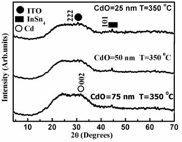
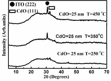
Figure shows the x-ray diffraction (XRD) patterns of annealed ITO films (350 °C) deposited at different CdO buffer layer thicknesses. The absence of any sharp diffraction peaks indicates the partially amorphous nature of these films. Only the small diffraction peaks (222), (002) and (101) corresponding to ITO, InSn4 and Cd, respectively, can be observed. Therefore, it is expected that as-deposited ITO films are also amorphous.
Figure 1 XRD patterns of ITO annealed at 350 °C and deposited onto CdO buffer layers of different thicknesses.
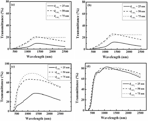
Transmittance T% spectra as a function of incident wavelength (200–2500 nm) for as-deposited and annealed ITO films with different CdO buffer layer thicknesses are shown in figure . It is observed that the transmittance of as-deposited ITO films (figure (a)) is low for all CdO layers. With increasing annealing temperature from 200 to 300 °C, a significant increase in transmittance is observed, as shown in figures (b) and (c). From figure (d), it is clear that the effect of CdO buffer layer thickness is not significant at temperature of 350 °C and the overall transmittance is almost the same (∼70%) as that in the visible region for all samples. The low transmittance of as-deposited films is due to the lack of oxygen resulting from deposition by electron beam evaporation. This result was noted in our previous works [Citation10, Citation17–19] and agrees with that in ref. [Citation23]. Moreover, the XRD pattern of ITO films confirms this result, as shown in figure .
Figure 2 Transmittance spectra (200–2500 nm) for (a) as-deposited and ITO films annealed at (b) 200 °C, (c) 300 °C, and (d) 350 °C and deposited onto CdO buffer layers of different thicknesses.
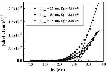
By the analysis of optical absorption spectra, it is found that the optical absorption edge is not sharply defined in the glass systems, clearly indicating their amorphous nature. In other words, the optical transmittances of as-deposited and annealed ITO films in the visible region at temperatures less than 300 °C are too small to use in determining the optical energy gap. Therefore, the optical energy gap, which is determined by extrapolating the linear portion of the plots of (αhν)2 versus hν to α=0 as shown in figure , has been calculated for ITO films annealed at a temperature of 350 °C. From this figure, it is observed that there is no significant variation in Eg with CdO buffer layer thickness.
Figure 3 Plot of (αhν)2 versus hν for ITO films annealed at 350 °C and deposited onto CdO buffer layers of different thicknesses.
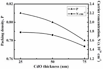
The extinction coefficient (k) and refractive index (n) as a function of CdO buffer layer thickness for annealed ITO films at 350 °C are shown in figure . It is observed that the extinction coefficient decreases with increasing CdO buffer layer thickness. This is expected on the basis of equation (2). It is also clear that the refractive index decreases with increasing CdO buffer layer thickness as shown in the recorded refractive indices of 2.15, 2.12 and 2.06 for the CdO buffer layer thicknesses of 25, 50 and 75 nm, respectively. This behavior can be attributed to the decrease in packing density. The dependences of packing density (p) and free carrier concentration (N) on the CdO buffer layer thickness of annealed ITO films at 350 °C are shown in figure . The packing density p was calculated using [Citation24, Citation25]:
(4)
where n is the refractive index of the prepared film that is calculated using equation (2), nS is the substrate refractive index and nV is the void refractive index (equal to one for air). On the other hand, the free carrier concentration also decreases with CdO buffer layer thickness, which can be attributed to the increase in transmittance in the near-infra region with CdO thickness [Citation14], as shown in figure .
Figure 4 Extinction coefficient (k) and refractive index (n) of ITO films annealed at 350 °C and deposited onto CdO buffer layers of different thicknesses.
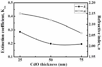
Figure 5 Dependences of packing density (p) and free carrier concentration (N) on thickness of CdO buffer layer of ITO films annealed at 350 °C.
The real (ε′) and imaginary (ε″) parts of the dielectric constant of annealed ITO films at 350 °C with different CdO thicknesses were calculated using equation (3) and plotted in figure as a function of wavelength in the near-infrared region. It is observed that the variations in ε′ and ε″ with wavelength obey Drude's theory. Moreover, it is obvious from figure (a) that the slopes of lines decrease with increasing CdO thickness, indicating a decrease in free carrier concentration, as discussed previously (figure ).
Figure 6 Plot of (a) real and (b) imaginary parts of dielectric constant as function of wavelength for ITO films annealed at 350 °C and deposited onto CdO buffer layers of different thicknesses.
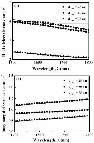
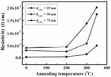
Figure shows the variations in the electrical resistivities of as-deposited and annealed ITO films with different CdO buffer layer thicknesses. It is noted that the increases in both CdO thickness and annealing temperature lead to an increase in film resistivity. The as-deposited ITO film with a CdO buffer layer thickness of 25 nm has the lowest resistivity of 4.7×10⁻⁴ Ω cm. With increasing temperature up to 350 °C, a significant increase in resistivity is observed, and the resistivity of the later film becomes 5.1×10⁻³ Ω cm. The increase in resistivity with CdO thickness is related to the decrease in free carrier concentration. The significant increase in resistivity at high temperatures may be caused by the removal of oxygen vacancies by the chemisorbed oxygen and the formation of grain boundaries acting as trap sites for free electrons [Citation26]. From these results, we can conclude that, in amorphous ITO films, electrical resistivity is more affected by the carrier density controlled by oxygen vacancies than by carrier mobility. Our results are in good agreement with those of Bae et al [Citation27].
Figure 7 Annealing temperature dependence of electrical resistivity of ITO films deposited onto CdO buffer layers of different thicknesses.
Effect of heat treatment of CdO layer
As indicated in the previous section, it was observed that the ITO film deposited onto the CdO buffer layer with a thickness of 25 nm has the lowest resistivity of 5.1×10⁻³–4.7×10⁻⁴ Ω cm and a high transmittance of 73% in the visible region (at 800 nm), whereas the annealed films at 350 °C has a transmittance of 83% in the NIR region (at 1100 nm). For these reasons, another set of CdO buffer layers with a thickness of 25 nm was deposited onto a silica glass substrate and heated at various temperatures of 250, 350 and 450 °C before the deposition of the second ITO layer with a thickness of 80 nm to further enhance the optical and electrical properties of ITO films.
Structure and morphology.
Figure shows the XRD patterns of ITO films deposited onto a thin CdO buffer layer with a thickness of 25 nm after heating at temperatures of 250, 350 and 450 °C. From this figure, it can be observed that the films exhibit two diffraction peaks of (222) and (111) for the cubic structures of ITO and CdO. As the heating temperature of the CdO buffer layer increases, the intensities of the observed peaks increase, indicating that the preferred orientations along (222) for ITO and (111) for CdO become stronger.
Figure 8 XRD patterns of ITO films deposited onto 25-nm-thick CdO layer heated at various temperatures.
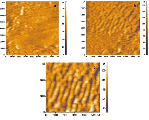
Figures (a)–(c) show AFM images of the same films. The images indicate that the surface morphologies and surface roughnesses of the films are affected by an increase in the heating temperature of the buffer layer. The grain size is increase by increasing the annealing temperature of the CdO buffer layer. This is in good agreement with XRD measurements (figure ), whereas the crystallinity of the films is increased by increasing the annealing temperature of the CdO buffer layer. Root mean square surface roughnesses (RMSs) are obtained by AFM and listed in table 1.
Figure 9 AFM images of ITO films deposited onto CdO-buffered glass heated at (a) 250, (b) 350 and (c) 450 °C.
Some optical properties of ITO films deposited onto 25-nm-thick CdO buffer layer heated at several temperatures.
Optical properties
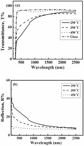
Figure shows the optical transmittance (T%) and reflection (R%) spectra of ITO films deposited onto the CdO buffer layers heated at temperatures of 250, 350 and 450 °C. It is noted that the increase in the temperature of the CdO buffer layer leads to a significant increase in transmittance, particular at a temperature of 450 °C. This behavior may be due to the improvement in the film structure. The average transmittances in the VIS and NIR regions are listed in table 1. It is clear that the transmittance attains its maximum value of about 91% in both VIS and NIR regions when the ITO films are deposited onto the CdO buffer layer annealed at 450 °C. These results should be compared with the transmittance of the glass substrate, as shown in this figure. On the other hand, the reflection of the ITO films decreases with increasing temperature. The decrease in the reflection of the ITO films with increasing annealing temperature of the CdO buffer layer can be attributed to the decreases in both the refractive index and packing density listed in table 1.
Figure 10 (a) Transmittance and (b) reflection spectra as function of incident wavelength of ITO films deposited onto 25-nm-thick CdO buffer layers heated at various temperatures.
The calculated direct optical energy gap as a function of the heating temperature of the buffer layer is listed in table 1. It is clear that Eg increases with increasing heating temperature and its maximum value of 3.61 eV is obtained at a temperature of 450 °C. The increase in optical energy gap is due to the increase in film transparency, which may be related to the improvement of film crystallinity. Since amorphous semiconductors are known to have band tails inside the energy gap, the transition of the band tails to the extended states can occur below the absorption edge [Citation26]. Due to these band tails and extended states, crystallized ITO films have a much greater optical band gap energy than amorphous films. Young [Citation28] has also reported a similar phenomenon in Zn2SnO4.
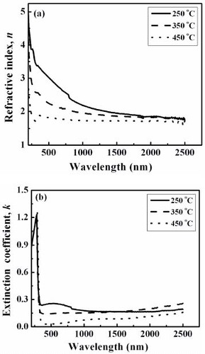
The wavelength dependences of refractive index and extinction coefficient are plotted in figures (a) and (b). It is observed that the refractive index decreases with increasing wavelength or heating temperature of the buffered layer, which can be attributed to the decrease in the packing density of the films listed in table 1. On the other hand, the decrease in extinction coefficient could be correlated to the decrease in absorption due to the increase in film transparency. The refractive index and extinction coefficient at a wavelength of 550 nm are listed in table 1.
Figure 11 (a) Wavelength dependences of refractive index and (b) extinction coefficient of ITO films deposited onto 25-nm-thick CdO buffer layers heated at various temperatures.
The fundamental absorption of films was described using the frequency-dependent complex electronic dielectric constant. The real and imaginary parts of the dielectric constant are provided by the relation (3) in terms of n and k. Figures (a) and (b) show the variations in the real and imaginary parts of the dielectric constant with wavelength in the NIR region (1700–1900 nm). It is generally noted that the dielectric constant decreases with increasing heating temperature of the buffered layer, indicating a decrease in the free carrier concentration listed in table 1.
Figure 12 Variations in (a) real and (b) imaginary parts of dielectric constant with wavelength in NIR region (1700–1900 nm) of ITO films deposited onto 25-nm-thick CdO buffer layers heated at various temperatures.
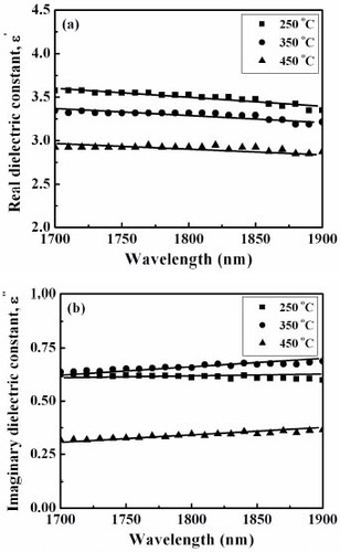
On the other hand, it is known that the imaginary part of the dielectric constant ε″ is directly related to the density of states within the forbidden gap of semiconductor materials [Citation29]. Comparing the ε″ values in figures (b) and (b), the above results indicate a decrease in the density of states within the forbidden gap and hence an increase in optical energy gap (as shown in table 1).
Refractive index dispersion plays an important role particularly in designing optical devices. Thus, it is important to determine dispersion parameters of the ITO films. According to the dispersion theory, the refractive index n of a dielectric medium in the region of low absorption is given by [Citation11, Citation30]
(5)
where n is the refractive index, h is Planck's constant, ν is the frequency, hν is the photon energy, Eo (single oscillator energy) is the average excitation energy for electronic transitions and Ed is the dispersion energy, which is a measure of the strength of an interband optical transition. By plotting (n2−1)−1 versus (hν)2 and fitting a straight line, Ed and Eo can be directly determined from the slope (EdEo)−1 and intercept Eo/Ed at the vertical axis. The obtained results are listed in table 1. It is noted that both Eo and Ed increase with temperature, owing to the behavior of energy gap [Citation31].
Electrical properties
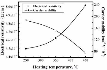
Figure shows the variations in the electrical resistivity ρ and carrier mobility μ of the ITO films deposited onto the heated CdO buffer layer with a thickness of 25 nm. It is clear that both ρ and μ vary with temperature in opposite manners, since ρ reaches its minimum value of 4.45×10⁻⁴ Ω cm and μ reaches its maximum value of 238 cm2 V−1 s−1 at a temperature of 450 °C. This indicates that carrier mobility is responsible for the decrease in electrical resistivity. The decrease in electrical resistivity or the increase in carrier mobility could be related to the improvement of ITO film crystallinity, as shown by x-ray results (figure ).
Figure 13 Variations in electrical resistivity and carrier mobility of ITO films with heating temperature of 25-nm-thick CdO buffer layers.
Conclusion
ITO thin films were deposited onto a CdO buffer layer by an electron beam evaporation technique. The effects of the thickness and heating temperature of the CdO buffer layer on the structural, optical and electrical properties of ITO films were investigated. It was found that the lowest CdO buffer layer thicknesses (25 nm) enhances the optoelectronic properties of ITO films. By increasing the heating temperature of the CdO buffer layer up to 450 °C, promising optical and electrical properties were obtained for ITO films. Since the optical transmittance reached 91% in the VIS and NIR regions, the optical energy gap attained was 3.61 eV and the electrical resistivity decreased up to 4.45×10⁻⁴ Ω cm at room temperature. The enhancement of the optical and electrical properties was mainly due to the improvement of film crystallinity. It was found that other optical properties, such as refractive index, extinction coefficient, real and imaginary parts of dielectric constant, dispersion energy, single effective oscillator energy, packing density and free carrier concentration, strongly depend on both CdO thickness and temperature.
Acknowledgments
The authors would like to acknowledge Professor M M Wakkad and Dr A K Diap for AFM measurements, which were performed in the Laboratory of Materials and Microelectronics of Provene, Faculty of Science and Technology of Scant Jerow, University of Paul Cesare, France. Also, we thank Mr M F Hasaneen for his help during this work.
References
- PaineD CWhitsonTJaniacDBeresfordRYangvC OLewisB 1999 J. Appl. Phys. 85 8445 http://dx.doi.org/10.1063/1.370695
- ChenB JSunX WTayB K 2004 Mater. Sci. Eng. B 106 300 http://dx.doi.org/10.1016/j.mseb.2003.09.046
- RajE SChoyK L 2003 Mater. Chem. Phys. 82 489 http://dx.doi.org/10.1016/S0254-0584(03)00278-5
- AliH MMohamedH AMohamedS H 2005 Eur. Phys. J. Appl. Phys. 31 87 http://dx.doi.org/10.1051/epjap:2005044
- SunX WWangL DKwokH S 2000 Thin Solid Films 360 75 http://dx.doi.org/10.1016/S0040-6090(99)01077-9
- GranqvistC GHultakerA 2002 Thin Solid Films 411 1 http://dx.doi.org/10.1016/S0040-6090(02)00163-3
- TagaNOdakaHShigesatoYYasuiIKameiMHaynesT E 1996 J. Appl. Phys. 80 978 http://dx.doi.org/10.1063/1.362910
- MorikawaHFujitaM 2000 Thin Solid Films 359 61 http://dx.doi.org/10.1016/S0040-6090(99)00749-X
- KameiMYagamiTTakakiSShigesatoY 1994 Appl. Phys. Lett. 64 2712 http://dx.doi.org/10.1063/1.111474
- MohamedH A 2007 J. Phys. D: Appl. Phys. 40 4234 http://dx.doi.org/10.1088/0022-3727/40/14/019
- AliH M 2005 Phys. Status Solidi a 202 2742 http://dx.doi.org/10.1002/pssa.200521045
- SunX WKimD HKwokH S 1997 Thin-Film Structure for Photovoltaics, Mater. Res. Soc. Symp. Proc. Vol 485 E DJones RNoufi B LSopori JKalejs Boston Materials Research Society p 267
- SunX WKwokH S 1999 J. Appl. Phys. 86 408 http://dx.doi.org/10.1063/1.370744
- HerreroJGuillénC 2004 Thin Solid Films 451–452 630 http://dx.doi.org/10.1016/j.tsf.2003.11.050
- SahaBThapaRChattopadhyayK K 2008 Solid State Commun. 145 33
- KulMZorMAybekA SIrmakSTuranE 2007 Solar Energy Mater. Sol. Cells 91 882 http://dx.doi.org/10.1016/j.solmat.2007.01.020
- MohamedH AAliH MMohamedS HAbd El-RaheemM M 2006 Eur. Phys. J. Appl. Phys. 34 7 http://dx.doi.org/10.1051/epjap:2006039
- AliH MMohamedH AWakkadM MHasaneenM F 2007 Thin Solid Films 515 3024 http://dx.doi.org/10.1016/j.tsf.2006.06.037
- AliH MMohamedH AWakkadM MHasaneenM F 2008 Japan. J. Appl. Phys. to be published
- XiuF XYangZZhaoD TLiuJ LAlimK ABalandinA AItkisM EHaddonR C 2006 J. Electron. Mater. 35 691 http://dx.doi.org/10.1007/s11664-006-0122-0
- TaucJ 1979 Amorphous and Liquid Semiconductors JTauc New York Plenum p 159
- WeijtensC H LVan loonP A C 1991 Thin Solid Films 196 1 http://dx.doi.org/10.1016/0040-6090(91)90169-X
- ChopraK LMajorSPandyaD K 1983 Thin Solid Films 102 1 http://dx.doi.org/10.1016/0040-6090(83)90256-0
- MacleodH A 1986 J. Vac. Sci. Technol. A 4 418 http://dx.doi.org/10.1116/1.573894
- AliH MAbd El-RaheemM MMegahedN MMohamedH A 2006 J. Phys. Chem. Solids 67 1823 http://dx.doi.org/10.1016/j.jpcs.2006.04.005
- KimI HKoJ HKimDLeeK SLeeT SJeongJ-HCheongBBaikY-JKimW M 2006 Thin Solid Films 515 2475 http://dx.doi.org/10.1016/j.tsf.2006.07.020
- BaeJ WKimH JKimJ SLeeN EYeonG Y 2000 Vacuum 56 77 http://dx.doi.org/10.1016/S0042-207X(99)00169-4
- YoungD L 2000 PhD Thesis Colorado School of Mines, USA
- WahabL AAmerH H 2006 Mater. Chem. Phys. 100 430 http://dx.doi.org/10.1016/j.matchemphys.2006.01.036
- YakuphanogluFCukurovaliAYilmazI 2004 Physica B 353 210 http://dx.doi.org/10.1016/j.physb.2004.09.097
- WempleS 1973 Phys. Rev. B 7 3767 http://dx.doi.org/10.1103/PhysRevB.7.3767