Abstract
Thin polycrystalline zinc-doped indium oxide (In2O3–ZnO) films were prepared by post-annealing amorphous films with various weight concentrations x of ZnO in the range 0x 0.06. We have studied the dependences of the resistivity ρ and Hall coefficient on temperature T and magnetic field H in the range 0.5T 300 K, H6 Tfor 350 nm films annealed in air. Films with 0x0.03 show the superconducting resistive transition. The transition temperature Tc is below 3.3 K and the carrier density n is about 1025–1026 m−3. The annealed In2O3–ZnO films were examined by transmission electron microscopy and x-ray diffraction analysis revealing that the crystallinity of the films depends on the annealing time. We studied the upper critical magnetic field Hc2 (T) for the film with x = 0.01. From the slope of dHc2 /dT, we obtain the coherence length ξ (0) ≈ 10 nm at T = 0 K and a coefficient of electronic heat capacity that is small compared with those of other oxide materials.
Introduction
Transparent electrode materials, such as In2O3 and tin-doped indium oxide (ITO), are well known and are already used in devices such as liquid crystal displays. Recently, amorphous indium zinc oxide (a-In2O3–ZnO) films have attracted considerable practical interest, because these films can give a smooth surface, which enables detailed processing with a high accuracy, and have large values of Hall mobility compared with a-In2O3 films. Some characteristics have been investigated, such as electrical resistivity [Citation1] and the effect of the substrate temperature on the mobility and morphology [Citation2] in a-In2O3–ZnO films. However, detailed studies of the transport properties at low temperatures are few. The electrical properties of a-In2O3–ZnO are very interesting from the viewpoint of quantum corrections in dirty systems with low carrier densities.
Recently, for a-In2O3–ZnO films, we have examined the electrical properties in the temperature range of 2 < T<300 K [Citation3]. For films with thickness d= 350 nm and weight concentration of ZnO x∼0.1, the temperature dependence of the resistivity ρ(T) shows metallic characteristics, that is, dρ/dT> 0, in a wide temperature range. However, we did not observe superconductivity in this temperature range. Although post-annealing in a vacuum does not increase the resistivity, annealing in air brings about a large resistivity change owing to the reduction of the carrier density n. Therefore we can consider that the free carriers are supplied by oxygen deficiency as well as by substitutional Zn. Concerning the effect of post-annealing in air on films with x = 0.1, it is reported that films annealed at 300 °C for 1 h have an amorphous structure [Citation4]. However, for films with x < 0.1, it is expected that the annealing effect in air improves the material properties. Indeed, annealing at 250–450 °C increases the resistivity and optical transparency of ITO films [Citation5]. The resistivity increase is associated with decreasing mobility. Higher transparency is important for optical applications; it was attributed to the improved crystallinity of the films. As for the appearance of superconductivity, Mori [Citation6] reported that ITO films attain a sharp superconducting transition by proper annealing and found that annealing at a relatively low temperature results in superconductivity. Recently, the superconductor-insulator transition in amorphous films of high carrier-density indium-oxide has been studied by Kowal and Ovadyahu [Citation7]. They reported that InxO films with n <1026 m-3 do not show superconductivity. Carrier density can be controlled by adjusting the annealing conditions; the new oxide material with lower carrier density than that observed up to now is expected to show superconductivity. For the purpose of finding a new type of superconductor with low carrier density, In2O3–ZnO is a suitable material.
In this work, we report superconductivity in In2O3–ZnO films prepared under certain annealing conditions. To clarify the occurrence of superconductivity, we have investigated the film structure by x-ray diffraction (XRD) analysis and high-resolution transmission electron microscopy (HRTEM). Further, we used electron energy-loss spectroscopy (EELS) in a TEM (TEM–EELS) to find the relationship between the transport characteristics and the micro- and nanostructure of the present materials.
Film preparation and experimental procedures
First, a-In2O3–ZnO films with d = 350 nm were prepared by dc-magnetron sputtering on glass substrates using the ceramic oxide In2O3–ZnO target under 0.3 Pa of Ar. We prepared several targets with different weight concentrations x of ZnO, x = 0.0, 0.005, 0.01, 0.02, 0.03, 0.04, 0.05 and 0.06. During deposition, the substrate was kept at room temperature. XRD reveals that these as-grown films have amorphous structure. The properties of In oxide films (structure, resistivity, etc) strongly depend on the deposition conditions. In particular, polycrystalline ITO films have been deposited without post-annealing by reactive magnetron sputtering [Citation8]. Although these films show metallic behavior, that is, dρ /dT> 0, in a wide temperature range, films show not superconductivity but insulating behaviors owing to localization or electron–electron effects at temperatures below 50 K.
We measured the temperature T and magnetic field H dependence of resistance R(T, H) by a standard dc four-probe technique. We applied H up to 6 T perpendicular to the film surface. Data on Hall coefficients RH were obtained in a standard manner. The photoresist lift-off method was used to obtain the necessary adequate pattern for Hall voltage. To eliminate the effect of Hall probe misalignment, measurements were performed in both positive and negative magnetic configurations. The results were averaged over the two perpendicular field orientations. For the Hall resistance, we confirmed that a linear dependence holds up to above H=±5 T. Electrical transport properties of resistivity ρ, carrier density n and mobility μ were measured from 0.5 to 300 K.
After deposition, we annealed the films in air. As the annealing temperature Ta, we adopted 200 and 300 °C. We annealed the films for a duration ta from 0.5 to 48 h by putting the glass substrate on a heated plate kept at a constant temperature within 0.5 K.
Experimental results and discussion
Figure shows the ρ (T) dependence at some external magnetic fields perpendicular to the surface of the film with x = 0.005 annealed at 300 °C for 2 h. The resistivity shows a drastic decrease at around 2 K, indicating the superconducting transition. We recognize the decrease of Tc by applying the external magnetic field. The inset shows ρ (T) at H = 0 and 5 T in a wide temperature range. Large negative magnetoresistivity is observed in a normal state temperature range. Figure (b) shows detailed data of the negative magnetoresistivity of the present In oxide systems at some temperatures near the onset of the superconductivity for In2O3 with x = 0 annealed at 300 °C for 2 h in N2 atmosphere. The superconducting transition temperature is around 0.5 K. Magnetoresistivity Δ ρ, defined as Δ ρ = [ρ (H) - ρ (0)]/ρ (0), initially increases owing to the destruction of superconductivity with increasing magnetic field. In stronger magnetic fields, Δ ρ becomes maximum at a certain value of Hm. At temperatures T < 2 K and fields H < 5 T, Δ ρ is positive in spite of d(Δ ρ)/dH < 0 at high fields. The value of Hm decreases with increasing temperature. At temperatures above 2.5 K, Δ ρ becomes negative at H> 2 T. Finally, at temperatures >6 K, Δ ρ becomes negative for any magnetic field. Although the positive Δ ρ at low fields and low temperatures mainly results from the destruction of superconductivity by the magnetic field, the quantum correction due to the electron localization and electron–electron interactions in dirty systems will give a dominant contribution to Δ ρ in a stronger magnetic field and at higher temperatures. In the case of weak spin orbit scattering, the correction brings about the negative magnetoresistivity. Such a negative Δρ in transparent oxide materials has been investigated in two- and three-dimensional a-In2O3–ZnO films [Citation3]. Then, the present results of Δ ρ are explained by the competition in the destructions of superconductivity and localization (and/or electron–electron interaction) by the magnetic field.
Figure 1 (a) T dependence of ρ of polycrystalline In2O3–ZnO film with weight concentration of ZnO x = 0.005 in various magnetic fields perpendicular to the film surface: H = 0, 0.1, 0.3, 1.0, 2.0, 3.0, and 4.0 T. The film was prepared by annealing as-grown amorphous In2O3–ZnO at 300 °C for 2 h. The inset shows the detailed data near the onset of superconducting transition at H=0 (•) and H = 5 T (○). (b) Normalized magnetoresistivity defined as Δ ρ = [ρ (H) - ρ (0)]/ρ (0) at temperatures T = 1.5, 2, 2.5, 3 and 3.5 K from top to bottom.
![Figure 1 (a) T dependence of ρ of polycrystalline In2O3–ZnO film with weight concentration of ZnO x = 0.005 in various magnetic fields perpendicular to the film surface: H = 0, 0.1, 0.3, 1.0, 2.0, 3.0, and 4.0 T. The film was prepared by annealing as-grown amorphous In2O3–ZnO at 300 °C for 2 h. The inset shows the detailed data near the onset of superconducting transition at H=0 (•) and H = 5 T (○). (b) Normalized magnetoresistivity defined as Δ ρ = [ρ (H) - ρ (0)]/ρ (0) at temperatures T = 1.5, 2, 2.5, 3 and 3.5 K from top to bottom.](/cms/asset/ed0f5b1c-978d-4dc2-aae1-80b7ef04d86d/tsta_a_11660803_f0001_oc.jpg)
Figure (a) shows the cross-sectional high angle annular dark-field scanning transmission electron microscopy (HAADF–STEM) image of the film with x = 0.005 annealed at 300 °C for 2 h. A cross-sectional TEM sample was prepared by a focused ion beam method. We can see the large grains separated by boundaries in the central part of the image. Figures (b) and (c) show the intensities of HAADF–STEM and EELS O-K edge line profile, respectively. These data were taken along the solid line of length ≈50 nm across the grain boundary in figure (a). The position indicated by the arrow in figure (b) corresponds to the crossing point with the grain boundary. The experimental result that the shapes of the line profiles in figures (b) and (c) are almost the same suggests that neither oxygen nor In aggregate at the grain boundary. As shown in figure (a), crystallized In2O3–ZnO films annealed at Ta = 300 °C show superconductivity. The transition temperature of films annealed at 300 °C lies between 0.5 and 2.0 K depending on the concentration x of ZnO. However, the value of Tc does not show a systematic change depending on x or annealing time ta, as far as the annealing temperature is chosen as Ta=300 °C. On the contrary, films annealed at Ta=200 °C show a systematic change of Tc depending on x and ta; the resistivity and transition temperature Tc monotonically increase with increasing ta for the investigated films with x = 0.005, 0.01 and 0.02.
Figure 2 (a) Cross-sectional HAADF-STEM image of grains and grain boundaries of In2O3–ZnO film with x = 0.05. (b) Intensity of HAADF–STEM and (c) EELS O-K edges. Line shows the profile taken on thick line crossing the grain boundary in HAADF–STEM image in (a). The point indicated by the arrow corresponds to the grain boundary.
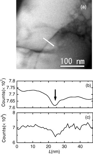
Figure (a) shows XRD patterns of films with x = 0.01 annealed at 200 °C for five different ta. The indexes correspond to the bixbite structure of In2O3 [Citation9]. It is found that the diffraction peak height increases with ta. In order to quantify the effect of annealing time on the crystallinity, we introduce a factor P from the analyses of the height of the XRD patterns as follows. Figure (b) shows the ta dependence of P(ta), which is defined by
(1)
where each Pi(ta) corresponds to the peak height of diffraction (211), (222), (400), (440) and (622) for the film annealed for ta. We observe crystallization even for the film annealed for only 0.5 h. The quantity P increases sharply for 0.5<ta<2 h and seems to saturate with ta>4 h. Figure (c) shows the TEM images for films annealed at 200 °C. As ta increases, the grain size increases. This finding is consistent with data shown in figures (a) and (b).
Figure 3 (a) XRD pattern of films annealed at 200 °C for different annealing times ta. (b) ta dependence of crystallinity factor P defined as P(ta) =∑Pi (ta)/∑ Pi (ta = 20 h). The quantity Pi (ta) corresponds to the peak height of diffractions (211), (222), (400), (440) and (622) for a film annealed for duration ta. (c) TEM images for films annealed at 200 °C for 0.5, 4.0 and 20 h.
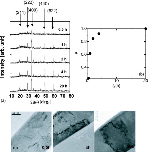
Figure (a) shows the ρ–T curves for films with different values of ta, where the data on a-In2O3–ZnO (ta = 0) film are also included. The resistivity ρ increases with increasing ta. Although the films annealed for 20 and 48 h show the insulating characteristic with dρ /dT < 0, other films show metallic behavior throughout the whole temperature range. All films, except a-In2O3–ZnO, exhibit the superconducting transition, as shown in figure (b).
Figure 4 (a) ρ (T) dependence for films with x = 0.01 annealed at 200 °C for 0 (amorphous), 0.5, 1.0, 2.0, 4.0, 20 and 48 h from bottom to top. (b) Normalized resistance R(T)/R(T = 4.2 K) for five films annealed for 0.5, 1.0, 2.0, 4.0 and 20 h from left to right.
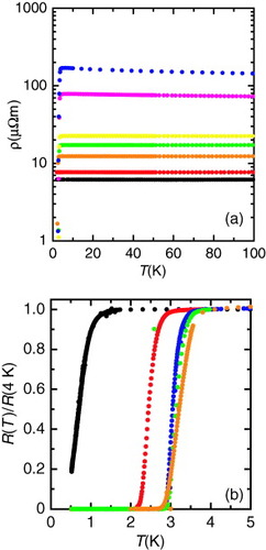
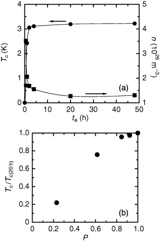
Figure (a) presents the ta dependence of Tc and carrier density n for films with x = 0.01 annealed at 200 °C. Although both Tc and n change drastically for short ta and apparently saturate with long ta, the two quantities show completely opposing behaviors. By annealing at 200 °C for several hours, carrier density n changes by about one-tenth. When we compare the carrier densities of the present films to those of previous materials showing superconductivity, the estimates in this work are smaller by a factor of 10–100. The mobility μ increases from 20 to 50 cm2 Vs-1 with ta increasing from 0 (amorphous film) to 4 h. Further increase of ta results in a gradual decrease of μ.
Figure 5 (a) Dependences of Tc (•) and n (▪) on annealing time ta for films with x = 0.01. The value of Tc was defined as the temperature at which half of the normal-state resistance was restored. (b) Dependence of Tc on crystallinity factor P.
We cannot explain this reverse behavior on the basis of the Bardeen–Cooper–Schrieffer theory, in which Tc is given by Tc = 1.13 ΘDexp(−1/gNF), where Θ D, g and NF are the Debye temperature, the coupling constant and the density of states at Fermi energy, respectively, if we assume constant g and the free electron model. As mentioned above, there is a possibility that the change in the crystal structure brings about superconductivity. Therefore, it is necessary to further study the crystal structure of each film annealed at different ta to further investigate the superconductivity.
From the ta dependences of P and Tc given in figures (b) and (a) for films with x = 0.01 annealed at 200 °C, we speculate on the effect of crystallization on Tc. Figure (b) shows the P dependence of normalized Tc, where P is defined in equation (1). The monotonic increase of Tc suggests that superconductivity of the present oxide films is dominated by the crystal structure and/or crystallinity for films annealed at 200 °C.
Using the data in figure (a), we show the n dependence of Tc in figure not only for films with x = 0.01 but also for films with x = 0.005 and 0.02. Within experimental error, Tc of our In oxide films is equal to or less than Tc of pure In metal (∼3.4 K). However, our critical magnetic fields are much higher than those of pure In ( 0.03 T). Therefore, superconductivity in our In oxide films cannot be assigned to metallic In channels. A similar decrease in Tc with carrier density was observed for In nitride films [Citation10]. In InN, the critical temperature decreases with carrier density n not only at high, but also at low n of approximately 4 × 10²³ m-3. The low-density decrease is associated with the Mott transition and it should be observed in In oxide films as well; it could not be verified in the present study because of the insufficiently low carrier density in our films. Although the exact value of Tc depends on x, the qualitative characteristics of Tc (n) are almost the same for three groups with different values of x = 0.005, 0.01 and 0.02. The value of Tc seems to increase as x increases for x 0.02 in the present work. However, it is expected that Tc will become maximum and then decrease as x increases further, because the films annealed at 300 °C do not show superconductivity for x> 0.03, as mentioned in the previous section.
Figure 6 Dependence of Tc on carrier concentration n for films with x = 0.005 (•), x = 0.01 (▪) and x = 0.02 (▴) annealed at 200 °C. The symbols on the horizontal axis are data of as-grown amorphous films.
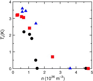
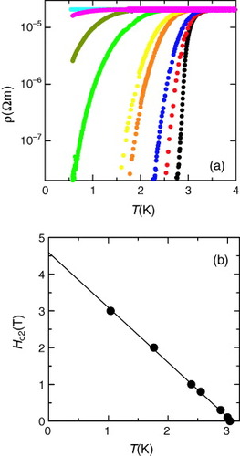
Figure (a) shows the typical ρ(T) dependence at various magnetic fields for the film with x= 0.02 annealed at 200 °C for 2 h. Figure (b) shows the temperature dependence of the upper critical magnetic field Hc2. According to the Ginzburg–Landau theory, the coherence length ξ(0) is given by
(2)
where φ 0 is the flux quantum (φ 0 = hc/2e = 2.07 × 10⁻¹⁵ Wb). From the value of |dHc2 /dT| determined in figure (b) and the above relation, we obtain the length ξ (0) ≈ 10 nm. Using the free electron model and the formula |(dHc2/dT)T≈Tc|= 4kB /π eD, where D is the diffusion constant and kB is the Boltzmann constant, we can also obtain the following relation for the coefficient of the electronic heat capacity γ as follows [Citation11],
(3)
where σ n is the normal-state conductivity. For the present film, γ ≈ 20 has been obtained using values of σ n and |(dHc2/dT)T≈Tc |. This value is small compared with that of pure In, γ ≈ 110. This finding is consistent with the low carrier density of the film, n∼ 8 × 1025 m-3.
Figure 7 (a) Tdependence of ρ of In2O3–ZnO with x = 0.01 annealed at 200 °C for 2 h at magnetic fields H = 0, 0.1, 0.3, 0.8, 1.0, 2.0, 3.0, 4.0 and 6.0 T. (b) T dependence of the upper critical magnetic field Hc2.
Conclusions
We have prepared polycrystalline In2O3–ZnO films from as-grown amorphous films by annealing in air, and observed superconductivity at temperatures below 3.3 K for films with restricted values x of the weight concentration of ZnO. EELS indicated no segregation of In at the grain boundaries. The critical temperature Tc and carrier concentration n of films with x = 0.01 annealed at 200 °C change systematically with annealing time. XRD patterns and the dependence of Tc on annealing time ta suggest that Tc correlates with the crystallinity.
From the slope of dHc2/dT and the conductivity of films with x = 0.01 annealed at 200 °C we have obtained the coherence length of ξ (0) ≈ 10 nm at T = 0 K and a small coefficient of the electronic heat capacity compared with that of other oxide materials.
Acknowledgment
We gratefully acknowledge with K Mitsuishi and K Iakoubovskii for stimulating discussions.
References
- MinamiTKasumuTTakataS 1996 J. Vac. Sci. Technol. A 14 1704 http://dx.doi.org/10.1116/1.580323
- JungY SSeoJ YLeeD WJeonD Y 2003 Thin Solid Films 445 63 http://dx.doi.org/10.1016/j.tsf.2003.09.014
- ShinozakiBMakiseKShimaneYNakamuraHInoueK 2007 J. Phys. Soc. Japan 76 074718 http://dx.doi.org/10.1143/JPSJ.76.074718
- SasabayashiTItoNNishimuraEKonMSongP KUtumiKKaijoAShigesatoY 2003 Thin Solid Films 445 219 http://dx.doi.org/10.1016/j.tsf.2003.08.047
- MohamedH AAliH M 2008 Sci. Technol. Adv. Mater. 9 025026 http://dx.doi.org/10.1088/1468-6996/9/2/025019
- MoriN 1993 J. Appl. Phys. 73 1327 http://dx.doi.org/10.1063/1.353251
- KowalDOvadyahuZ 2008 Physica C 4 322 http://dx.doi.org/10.1016/j.physc.2007.07.012
- OhnoSKawagutiYMiyaharaASatoYSongP KYoshikawaMFrachPShigesatoY 2006 Sci. Technol. Adv. Mater. 7 56 http://dx.doi.org/10.1016/j.stam.2005.11.005
- YagliogluBHuangY JYeomY HPaineD C 2006 Thin Solid Film 496 89 http://dx.doi.org/10.1016/j.tsf.2005.08.255
- InushimaT 2006 Sci. Technol. Adv. Mater. 7 S112 http://dx.doi.org/10.1016/j.stam.2006.05.009
- Saint-JamesDSarmaGThomasE J 1969 Type II Superconductivity (International series of monographs in Nature Philosophy) vol 19 THaar Oxford Pergamon p 174