
Abstract
The single-layer graphene has attracted considerable attention for the promising applications in new generation nanoelectronics and optoelectronics devices because of the high deal carrier mobility. Present investigations deal with the effect of chemical/molecular doping with varying the concentration of strong electron acceptor molecule such as tetracyanoethylene (TCNE) on transfer characteristics of single-layer graphene transistor. The Dirac point shift toward the positive gate voltage as a function of increasing concentration of TCNE molecules clearly indicates that the graphene is P-type doped. Our results indicate that the fermi energy level can be controlled by the amount of molecular doping in order to obtain graphene transistors with tunable Dirac points, which can be easily configured into functional nanoelectronic devices.
Introduction
Single-layer graphene is the thinnest electronic material discovered recently through the micromechanical cleavage technique from the bulk graphite crystal.Citation1–Citation5 It has been attracted considerable attention from the scientific community for its fundamental research and potential applications because of its fascinating structural,Citation1–Citation3 optical,Citation4 electronic,Citation1,Citation2,Citation6–Citation11 and magnetic properties.Citation12 In particular, being as a two-dimensional (2D) sheet, its conduction and valence bands touch at the Dirac points in the six corners of the hexagonal Brillouin zone, which makes graphene semimetal.Citation1,Citation2 Further, the low-energy excitations are massless Dirac fermions near the Dirac points. These properties make graphene very interesting material with enormously high carrier mobility up to 2 × 105 cm2/ Vs.Citation1–Citation3,Citation6–Citation11 Further, this makes graphene as an ideal material for future nanoelectronics device applications.Citation6–Citation11 However, owing to the lack of a band gap in pristine single-layer graphene, the transistor devices possess a low ION/OFF ratio and therefore hinders its applications to switch off the electronic devices. Thus, it is essential to have an energy band gap in the single-layer graphene sample to further enhance the ION/OFF ratio for its possible application in logic and digital nanoelectronics devices.
Recently, there are attempts by researchers to open a band gap in graphene using lateral quantum confinement,Citation10 hydrogenation,Citation13 breaking the inversion symmetry in bilayer grapheme, and making graphene nanoribbon.Citation14 Owing to this, the mobility in graphene sample was limited by the strapping edge scattering. On the other hand, the band gap can also be generated either by applying an external electric field normal to the single-layer graphene sheetCitation2,Citation3 or by the charge–transfer doping from the adsorbed strong electron donor or acceptor molecules or by the metal atoms decoration.Citation15–Citation24 In general, the gate bias is limited by the insufficient strength of SiO2/Si gate dielectric materials. The charge–transfer doping by the electron donor and acceptor molecules or decoration using metal atoms can create an interlayer electric field, which foremost to an opening of band gap in graphene.Citation21 It is well known that the decoration of metal atoms on graphene surface may not be homogeneous if it is done by the physical mixing. This further brings the issues and challenges related to the charge impurities in the graphene transistor device and drastically fall the mobility of transistor device. The non-homogeneous nature of the metal atom decoration can be avoided by the molecular doping using powerful electron donor and acceptor organic molecules dispersed in suitable organic solvents. The adsorption of electron donor and acceptor molecules may not impair the π-bonding networks of graphene, and thus the mobility in the device can largely be conserved. For charge–transfer doping, the organic molecules can be directly deposited on the surface of graphene sheet, and thus the band gap opening has some control depending on the concentration of molecule. The molecules adsorbed on the surface of graphene sheet are strongly influenced by supporting SiO2/Si substrate. It is well known that the graphene on SiC leads to n-type doping,Citation25,Citation26 while graphene on amorphous SiO2/Si leads to a p-type doping because of the adsorbed O2/water molecules between the interaface.Citation27,Citation28 Further, it has been reported that the single-layer graphene sample is hundred times more chemically reactive than the thicker graphene sheets.Citation29–Citation31 Therefore, controlling the functionalization of graphene sheets will be a challenging task and therefore, it may be the source of even more specific properties and applications.
Motivated by above experiments, author fabricated a single-layer graphene transistor devices using E-beam lithography which where doped with a strong electron acceptor organic molecule such as tetracyanoethylene (TCNE) with a varied concentration. This makes graphene transistor more p-type as evidenced by the shift in the Dirac point toward the positive gate voltage.
The organic molecule TCNE is chosen in current experiment for doping graphene because it often used as a very powerful electron acceptor molecule. The cyano groups (consists of a carbon atom triple-bonded to a nitrogen atom) present in the TCNE molecule have low-energy π orbitals, and the presence of four such groups, with their π systems linked to the central C = C double bond, gives rise the TCNE molecule to an excellent electron acceptor molecule.
Experimental methods
Single-layer graphene sheets were deposited at ambient condition by mechanically exfoliating bulk graphite (SPI Supplier, USA) on to SiO2 (300 nm)/Si substrates as reported earlier.Citation1–Citation3 The single-layer graphene sheets were first identified using optical microscope (total magnification of × 1000). The exfoliated single-layer graphene flakes had typical dimensions of tens of micrometres and thickness < 0.5 nm. The as-synthesized single-layer graphene sample was further characterized by the Atomic Force Microscope (Bruker ICON) and Raman spectroscopy system (Nano-photon Raman-11). In Raman spectroscopy, the 532-nm line of an Ar ion laser was used as the excitation source with a laser power of ∼1 mW. The laser beam was focused onto the sample by a × 100 objective lens and the scattered light was collected in the backscattering geometry. The collected scattered light was dispersed by spectrometer grating of 2400 mm and was detected with an electrically cooled CCD detector. The spatial resolution was < 0.8 μm, and the spectral resolution was 1.6 cm− 1 with a peak position accuracy of 0.1 cm− 1. After identifying and confirming single-layer graphene sheets, the electrodes were fabricated using standard electron beam lithography method. In brief, first the single-layer graphene samples on 300 nm SiO2/Si were spin-coated with PMMA (2% concentration in anisole, 4000 RPM for 45 s) followed by baking at 180° C for 1 min and exposed to a focused 30 keV electron beam in FEI Quanta ESEM. After the development in MIBK : IPA 1 : 3 solution for 75 s, the contact materials were evaporated (Ti/Au, 1/70 nm thickness) and performed the lift-off in acetone (30 min on a hot plate at 45° C). The heavily doped silicon substrates were used as the back gate. Electrical characterization of various single-layer graphene field-effect transistor devices were carried out using a Keithley 4200 semiconductor characterization system with a shielded probe station attached with micromanipulator in ambient air and then in a vacuum of 10− 6 mbar. Various concentrations of TCNE were prepared by dissolving a 12.8 mg of TCNE in 1 mL of benzene to attain 10− 1M concentration. Solutions of lower concentrations were further prepared by dilution using benzene. These solutions were further spin-coated onto the surface of single-layer graphene transistors. The atomic force microscopy (AFM) images were recorded before and after the evaporation of the solutions at room temperature.
Results and discussion
For molecular charge–transfer interaction investigations based on single-layer graphene transistor, initially the mechanically exfoliated graphene sample was prepared on 300 nm SiO2/Si wafer by using scotch-tape method.Citation1–Citation3 The number of layers present in the graphene sample were calculated using optical microscopy and confirmed by the Raman spectroscopy and the AFM. The number of layers present in the graphene sheet sample were initially determined using the color contrast with the help of an optical microscope and further confirmed by the AFM and using the shape and characteristic bandwidth of the Raman 2D-band spectrum of graphene (∼2680 cm− 1). The Raman spectroscopy of a typical single-layer graphene sample showed a sharp and single 2D-band with a full width at half maximum (FWHM) of ∼30 cm− 1, whereas broader 2D-bands were observed for the few-layer graphene sample.
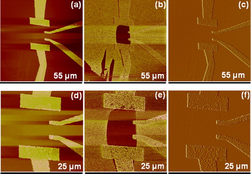
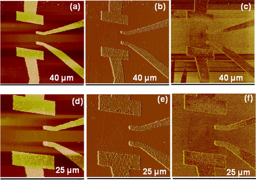
shows the typical Raman spectrum of a single-layer graphene (inset shows optical image of the single-layer graphene). The absence of defect related D-band at ∼1350 cm− 1 indicates that the highly crystalline nature of the single-layer graphene sample. shows the typical AFM image of the single-layer graphene sample deposited onto 300 nm SiO2/Si substrate and shows the corresponding AFM height profile depicting the height of ∼0.5 nm, which indicates the single-layer nature of graphene sample. The Raman spectroscopy was also carried out on a single-layer graphene with varying the concentration of TCNE in it. Both the G-band and 2D-band of graphene show a substantial shift in the Raman peak which indicates the p-type doping in the graphene sample.Citation22 It can be noted that the graphene with high defect sample can also be doped using powerful electron donor or acceptor organic molecules but with a less magnitude of doping. Where in the case of defect-free graphene sample, the magnitude of doping is observed to be high as confirmed by the earlier reports, where the large shift in G-band and 2D-band was observed.Citation22 Further, confirming whether graphene really doped using organic molecules such as TTF/TCNE and make graphene sample more p-type or n-type, several single-layer graphene field-effect transistor devices were fabricated using electron beam lithography and investigated their transfer characteristics using molecular interaction. shows the typical optical image of the defect-free single-layer graphene sample before patterning the electrode. shows the optical image of the same sample after patterning the electrode. show the typical SEM images of the same single-layer graphene field-effect transistor device. show the typical AFM height profiles of the single-layer graphene field-effect transistor device after annealing at 500° C at H2 + Ar atmosphere. are the typical AFM phase images and are the AFM amplitude error images shown for the clarity.
Figure 1. a Raman spectrum of a single-layer graphene (inset shows the optical image of single-layer graphene). b Atomic force microscopy (AFM) image of the single-layer graphene and c corresponding AFM height profile shows a height of ∼0.5 nm, indicating the single-layer nature of graphene sample
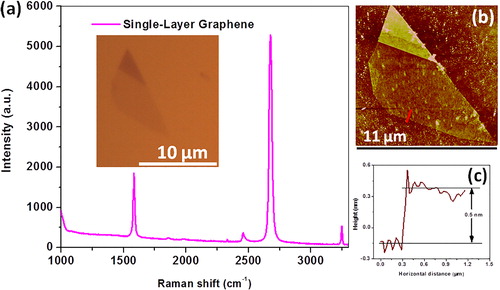
Figure 2. Typical optical images of single-layer graphene a before patterning the electrode and b after patterning the electrode. c, d Typical SEM images of the single-layer graphene field-effect transistor
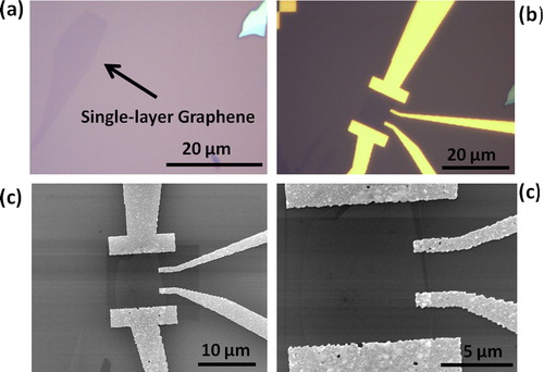
Figure 3. Typical atomic force microscopy (AFM) images of single-layer graphene field-effect transistor after annealing at a temperature of 500°C at H2 + Ar atmosphere: aand d height profile image, b and e phase image, and c and f amplitude error image
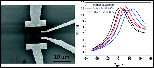
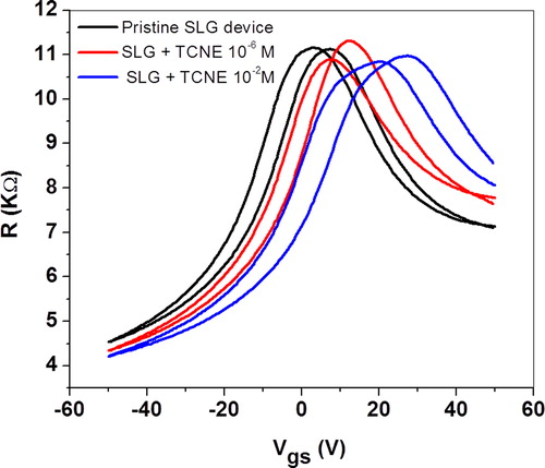
shows the constant mobility of charge carriers in single-layer graphene transistor with an increasing concentration of TCNE doping. The parallel shift indicates a negligible scattering effect of the charged impurities induced by the molecular charge–transfer doping in the single-layer graphene transistor. The curves are fast sweeps to Vg ± 50 V (with a sweep rate of 1 V/s) from each point. It is important to note that the position of the resistance peak (Dirac point) depends on the concentration of TCNE. With increasing the concentration of TCNE, a clear shift in the Dirac point toward the positive gate voltage is evident, which indicates that the graphene is more p-type. The shift in Dirac point position as a function of TCNE concentration indicates that the magnitude of doping increases with increasing concentration of TCNE. Meanwhile, the gate voltage corresponding to the Dirac point, the valley point in the transfer curve, is 5.5 V in an ambient condition and increases to 8.3 V (10− 6M) and 22.9 V (10− 2M) after TCNE interaction suggests that the single-layer graphene device is strongly doped.Citation22,Citation26,Citation27 It is further important to note that after the decoration of TCNE molecule on graphene surface results in the slight shift of Fermi level. Another important notable change in the transfer curve after decoration of TCNE is the constant mobility. The field-effect mobility of holes was calculated from the slope of dIds/dVgs, fitted to the linear part of the transfer curves using the equationCitation27,Citation28where Ci is the capacitance per unit area between the conducting channel and the back gate (Ci = ε0εr//d; εr = 3.9 for SiO2; d is the thickness of insulating 300 nm SiO2 layer), L is the channel length, W is the channel width. The hole mobility in ambient was observed to be ∼4300 cm2/Vs after decoration of TCNE. It is important to note that the field-effect mobility values can be higher if obtained by using the Hall effect measurements.
Figure 4. Typical transfer characteristics of the single-layer graphene transistor before and after TCNE decoration. The curve clearly shows the constant mobility of charge carriers in a single-layer graphene transistor with increasing chemical doping. The parallel shift indicates a negligible scattering effect of the charged impurities induced by the molecular charge–transfer doping in single-layer graphene. The curves are fast sweeps to a Vgs ± 50 V (with sweep rate of 1 V/s) from each point with Vds = 500 mV. They show that the position of the resistance peak (Dirac point) depends on the concentration of the TCNE.
For organic molecular doping experiments, the organic molecules such as TCNE were prepared in suitable solvents with varying concentration and then deposited on the top surface of graphene device by spin coating or by drop casting of solvent. shows the typical AFM image of the single-layer graphene before the addition of TCNE. and c are the corresponding AFM phase and amplitude error images shown for more clarity. is the AFM height images of single-layer graphene after addition of (doping) TCNE solution with concentration 10− 2M and the corresponding AFM phase images are shown in , and the AFM amplitude error images were shown in . shows the AFM images of single-layer graphene transistor devices after addition of (doping) TCNE 10− 2M (a–d) height profile images, (b, e) phase images and (c, f) amplitude error images. From AFM images of TCNE-decorated graphene sample, it has been clearly observed that the thickness of the sample was slightly increased because of a non-uniform coverage of TCNE molecule. It is important to note that after the evaporation of TCNE solvent, some randomly distributed TCNE particles forms the island-like growth structure on the graphene sheet surfaces.
Figure 5. a Typical atomic force microscopy (AFM) image of the single-layer graphene before addition of tetracyanoethylene (TCNE), b and c are corresponding phase and amplitude error images. The AFM image of the single-layer graphene after addition of (doping) TCNE 10− 2 M concentration solution (d and g) and corresponding phase images (e and h), and amplitude error images f and i)
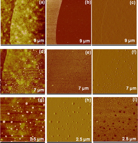
Figure 6. Atomic force microscopy (AFM) images of single-layer graphene transistor devices after addition of (doping) tetracyanoethylene (TCNE) 10− 2 M height profile images (a–d), phase images (b, e), and amplitude error images (c, f)
Conclusion
In conclusion, charge–transfer doping caused by an interaction with strong electron acceptor TCNE molecules affects the transfer curve of the field-effect transistor device of a single-layer graphene. It is shown that the TCNE acts as strong electron acceptor molecule, which makes graphene to a more p-type. The shift in the Dirac points toward positive gate voltage as a function of increasing concentration of TCNE indicates the magnitude of doping increases with increasing in concentration. The performance of our single-layer graphene transistors can be improved by reducing the defects and damage creation during preparation and transfer processes to meet the requirements of various device applications including thin film solar cells, flexible touch screen panels and nanoelectronic papers.
Acknowledgments
The author would like to thank Prof. C. N. R. Rao (FRS) (Director ICMS, Bangalore, India) and Prof. Vinayak P. Dravid (Director, NUANCE NWU, USA) for support and encouragement. Dr D. J. Late would like to thank Department of Science and Technology (Government of India) for a Ramanujan Fellowship (Grant No. SR/S2/RJN-130/2012). The research work was primarily supported by NCL-MLP project grant 028626, DST-SERB Fast-track Young Scientist project Grant No. SB/FT/CS-116/2013 and the partial support by INUP IITB project sponsored by DeitY, MCIT, Government of India.
Conflicts of interest
The author declares that there are no conflicts of interest.
References
- Novoselov K. S., Jiang D., Schedin F., Booth T. J., Khotkevich V. V., Morozov S. V. and Geim A. K.: ‘Two-dimensional atomic crystals’, Proc. Natl. Acad. Sci. U.S.A., 2005, 102, 10451–10453.
- Novoselov K. S., Geim A. K., Morozov S. V., Jiang D., Zhang Y., Dubonos S. V., Grigorieva I. V. and Firsov A. A.: ‘Electric field effect in atomically thin carbon films’, Science, 2004, 306, 666–669.
- Novoselov K. S., Geim A. K., Morozov S. V., Jiang D., Katsnelson M. I., Grigorieva I. V., Dubonos S. V. and Firsov A. A.: ‘Two-dimensional gas of massless Dirac fermions in graphene’, Nature, 2005, 438, 197–200.
- Blake P., Hill E. W., Castro Neto A. H., Novoselov K. S., Jiang D., Yang R., Booth T. J. and Geim A. K.: ‘Making graphene visible’, Appl. Phys. Lett., 2007, 91, 63121–63124.
- Late D. J., Maitra U., Panchakarla L. S., Waghmare U. V. and Rao C. N. R.: ‘Temperature effects on the Raman spectra of graphenes: dependence on the number of layers and doping’, J. Phys. Condens. Matter, 2011, 23, 055303.
- Late D. J., Ghosh A., Subrahmanyam K. S., Krupanidhi S. B., Panchakrla L. S. and Rao C. N. R.: ‘Characteristics of field-effect transistors based on undoped and B- and N-doped few-layer graphenes’, Solid State Commun., 2010, 150, 734–738.
- Ghosh A., Late D. J., Panchakarla L. S., Govindaraj A. and Rao C. N. R.: ‘NO2 and humidity sensing characteristics of few-layer graphene’, J. Exp. Nanosci., 2009, 4, 313–322.
- Du X., Skachko I., Barker A. and Andrei E. Y.: ‘Approaching ballistic transport in suspended graphene’, Nat. Nanotechnol., 2008, 3, 491–495.
- Morozov S. V., Novoselov K. S., Katsnelson M. I., Schedin F., Elias D. C., Jaszczak J. A. and Geim A. K.: ‘Giant intrinsic carrier mobilities in graphene and its bilayer’, Phys. Rev. Lett., 2008, 100, 016602.
- Berger C., Song Z., Li X., Wu X., Brown N., Naud C., Mayou D., Li T., Hass J., Marchenkov A. N., Conrad E. H., First P. N. and de Heer W. A.: ‘Electronic confinement and coherence in patterned epitaxial graphene’, Science, 2006, 312, 1191–1196.
- Bai J., Zhong X., Jiang S., Huang Y. and Duan X.: ‘Graphene nanomesh’, Nat. Nanotechnol., 2010, 5, 190–194.
- Wang Y., Huang Y., Song Y., Zhang X., Ma Y., Liang J. and Chen Y.: ‘Room-temperature ferromagnetism of graphene’, Nano Lett., 2009, 9, 220–224.
- Elias D. C., Nair R. R., Mohiuddin T. M. G., Morozov S. V., Blake P., Halsall M. P., Ferrari A. C., Boukhvalov D. W., Katsnelson M. I., Giem A. K. and Novoselov K. S.: ‘Control of graphene's properties by reversible hydrogenation: evidence for graphane’, Science, 2009, 323, 610–613.
- Khare R., Shinde D. B., Bansode S., More M. A., Majumder M., Pillai V. K. and Late D. J.: ‘Graphene nanoribbon as prospective field emitter’, Appl. Phy. Lett., 2015, 106, 023111.
- Zhang W., Lin C. T., Liu K. -K., Tite T., Su C. Y., Chang C. H., Lee Y. H., Chu C. -W., Wei K. -H., Kuo J. L. and Li L. J.: ‘Opening an electrical band gap of bilayer graphene with molecular doping’, ACS Nano, 2011, 5, 7517–7524.
- Xia F., Farmer D. B., Lin Y. and Avouris P.: ‘Graphene field-effect transistors with high on/off current ratio and large transport band gap at room temperature’, Nano Lett., 2010, 10, 715–718.
- Yu W. J., Liao L., Chae S. H., Lee Y. H. and Duan X. F.: ‘Toward tunable band gap and tunable Dirac point in bilayer graphene with molecular doping’, Nano Lett., 2011, 11, 4759–4763.
- Park J., Jo S. B., Yu Y. -J., Kim Y., Yang J. W., Lee W. H., Kim H. H., Hong B. H., Kim P., Cho K. and Kim K. S.: ‘Single-gate bandgap opening of bilayer graphene by dual molecular doping’, Adv. Mater., 2012, 24, 407–411.
- Ohta T., Bostwick A., Seyller T., Horn K. and Rotenberg E.: ‘Controlling the electronic structure of bilayer graphene’, Science, 2006, 313, 951–954.
- Dong X., Fu D., Fang W., Shi Y., Chen P. and Li L.: ‘Doping single-layer graphene with aromatic molecules’, Small, 2009, 5, 1422–1426.
- Wehling T. O., Novoselov K. S., Morozov S. V., Vdovin E. E., Katsnelson M. I., Geim A. K. and Lichtenstein A. I.: ‘Molecular doping of graphene’, Nano Lett., 2008, 8, 173–177.
- Late D. J., Ghosh A., Chakraborty B., Sood A. K., Waghmare U. V. and Rao C. N. R.: ‘Molecular charge-transfer interaction with single-layer graphene’, J. Exp. Nanosci., 2011, 6, 641–651.
- Wang T. H., Zhu Y. F. and Jiang Q.: ‘Bandgap opening of bilayer graphene by dual doping from organic molecule and substrate’, J. Phys. Chem. C, 2013, 117, 12873–12881.
- Gierz I., Riedl C., Starke U., Ast C. R. and Kern K.: ‘Atomic hole doping of graphene’, Nano Lett., 2008, 8, 4603–4607.
- Zhou S. Y., Gweon G. -H., Fedorov A. V., First P. N., De Heer W. A., Lee D. -H., Guinea F., Castro Neto A. H. and Lanzara A.: ‘Substrate induced bandgap opening in epitaxial graphene’, Nat. Mater., 2007, 6, 770–775.
- Ryu S., Liu L., Berciaud S., Yu Y. -J., Liu H., Kim P., Flynn G. W. and Brus L. E.: ‘Atmospheric oxygen binding and hole doping in deformed graphene on a SiO2 substrate’, Nano Lett., 2010, 10, 4944–4951.
- Late D. J., Liu B., Matte H. S., Dravid V. P. and Rao C. N. R.: ‘Hysteresis in single-layer MoS2 field effect transistors’, ACS Nano, 2012, 6, 5635–5641.
- Late D. J., Huang Y., Liu B., Acharya J., Shirodkar S. N., Luo J., Yan A., Charles D., Waghmare U. V., Dravid V. P. and Rao C. N. R.: ‘Sensing behavior of atomically thin-layered MoS2 transistors’, ACS Nano, 2013, 7, 4879–4891.
- Diankov G., Neumann M. and Goldhaber-Gordon D.: ‘Extreme monolayer selectivity of hydrogen-plasma reactions with graphene’, ACS Nano, 2013, 7, 1324–1332.
- Shi Y., Fang W., Zhang K. and Li L. J.: ‘Photoelectrical response in single-layer graphene transistors’, Small, 2009, 5, 2005–2011.
- Zhang W. and Li L. J.: ‘The screening of charged impurities in bilayer graphene’, New J. Phys., 2010, 12, 103037.