Figures & data
Table 1 Plasma spraying parameters for the manufacture of Er2Si2O7 coatings.
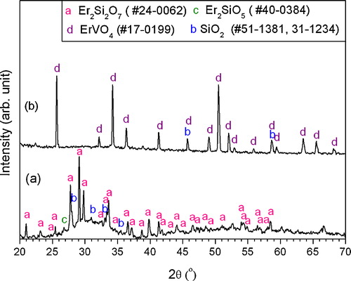
Fig. 1 XRD patterns of (a) Er2Si2O7 powders fabricated by solid-state reaction at 1450 °C for 22 h and (b) as-sprayed Er2Si2O7 coating deposited on Cf/SiC composites coupon.
Fig. 2 Variation in the coefficient of thermal expansion (CTE) and thermal expansion rate (ΔL/L0) with temperature for Er2Si2O7 bar by dilatometry. The bar was sintered at 1500 °C for 5 h prior to dilatometric measurements.
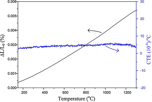
Fig. 3 (a) Macrograph of as-sprayed Er2Si2O7 coating on the Cf/SiC coupon, (b) SEM image on the surface of as-sprayed Er2Si2O7 coating and (c–d) EDS analysis for point 1 located in the flattened splat and point 2 located in the accumulated incongruent molten media within the as-sprayed Er2Si2O7 coating, respectively.
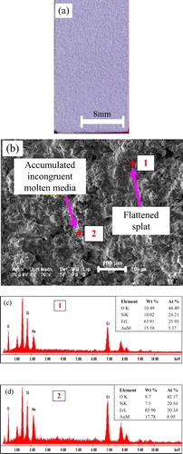
Fig. 4 (a) SEM image on the cross-section of as-sprayed Er2Si2O7 coating on Cf/SiC coupon, (b) EDS line scan starting from the interlayer and terminating at the surface of the coating, and (c–d) EDS spectra along with elemental percentages for point A near the interface and point B near the surface of the coating, respectively.
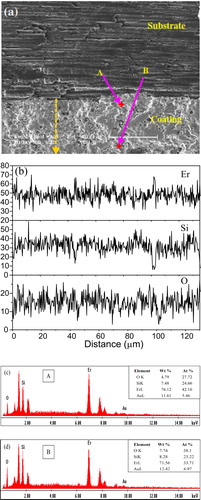
Fig. 5 (a) SEM image on the surface of the thermal shock tested Er2Si2O7 coating on Cf/SiC coupon, (b) camera photograph of the thermal shock tested Er2Si2O7 coating on Cf/SiC coupon, and (c–e) EDS analysis for point A located in the flattened splat, point B in the accumulated media and point C in the sponge-like media in (a), respectively.
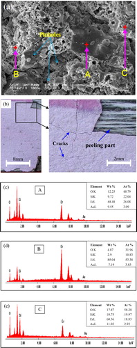
Fig. 6 (a) SEM image on the cross-section of the thermal cycled Er2Si2O7 coating on Cf/SiC coupon and (b and c) EDS spectra along with elemental percentages for point A near the interface and point B near the surface, respectively.
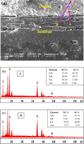
Fig. 7 XRD patterns of (a) as-sprayed Er2Si2O7 coating and (b) the thermally cycled Er2Si2O7 coating with 327 cycles with a flame temperature of 2000 °C. For each cycle, the coating was thermal cycled between surface temperatures of 400 °C and 1500 °C. (a) repeated for the sake of ease in comparison to the readers.
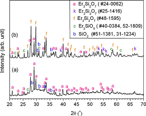
Fig. 8 (a) SEM image on the surface of plasma sprayed Er2Si2O7 coating after exposure to molten V2O5 for 6 h at 800 °C and (b and c) EDS analysis for points 1 and 2 in (a), respectively.
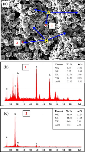
Fig. 9 XRD patterns of (a) the as-sprayed Er2Si2O7 coating and (b) the coating after exposure to molten V2O5 salt for 6 h at 800 °C. (a) repeated again for the sake of ease in comparison to the readers.