
Figures & data
Figure 1. Categories of launched nanosatellites.
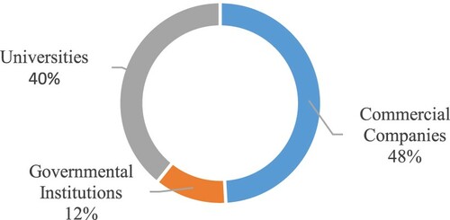
Figure 2. Design process for EPS of CubeSat.
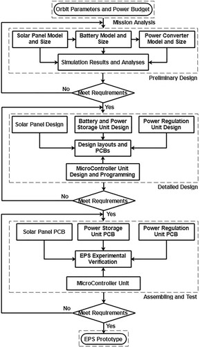
Figure 3. 1U CubeSat structure [Citation27].
![Figure 3. 1U CubeSat structure [Citation27].](/cms/asset/1098b63c-9a0d-4906-98a9-d99478ecd681/taut_a_2065420_f0003_oc.jpg)
Table 1. Mission parameters.
Table 2. Power consumption of subsystems.
Table 3. Power of different mission modes.
Figure 4. Mission power consumption profile, baseline scenario (worst-case).
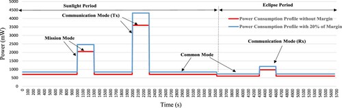
Figure 5. Proposed EPS configuration for CubeSat with open solar panels structure.
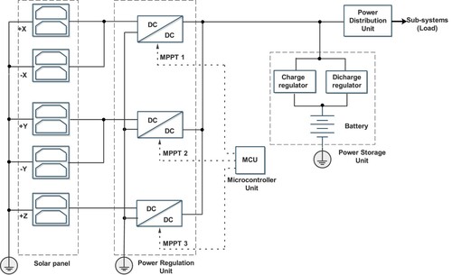
Figure 6. Flowchart of the implemented control strategy.
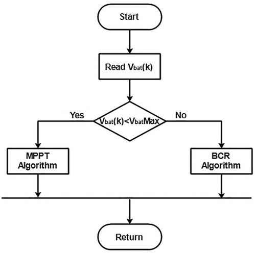
Figure 7. AzurSpace PV cell characteristics influenced by temperature: Curves of current and power versus voltage.
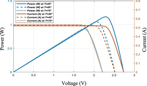
Figure 8. Proposed connection of solar cells for PV panel.
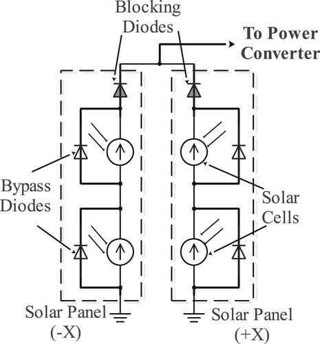
Figure 9. PV panel characteristics based on AzurSpace solar cells influenced by temperature: Curves of current and power versus voltage.
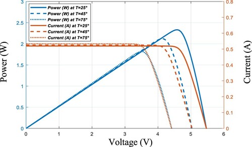
Figure 10. Generated power as a function of incident light angles: (a) Ideal case;(b) Worst case.
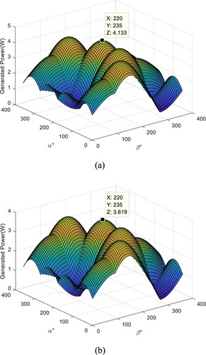
Figure 11. Solar panel PCB.
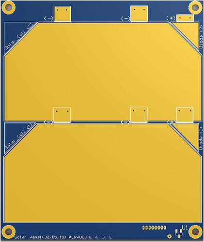
Table 4. Review of the Space commercially available Li-ion cell chemistries and their characteristics [Citation44].
Figure 12. Discharge characteristics of rechargeable LiFePO4 APR18650M1A battery.
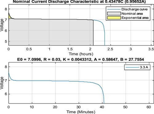
Figure 13. Electrical schematic of the Power Storage Unit.
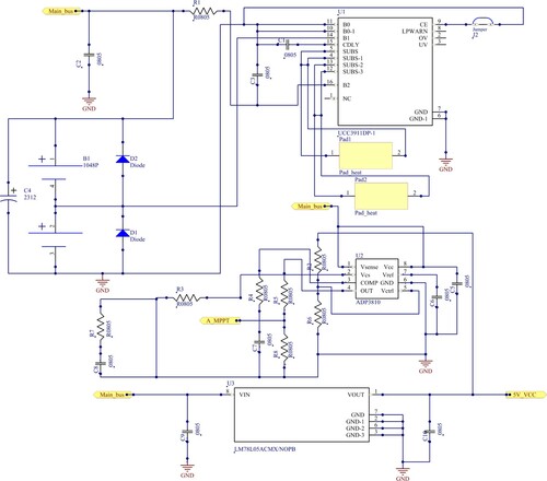
Figure 14. Power Storage Unit’s PCB.
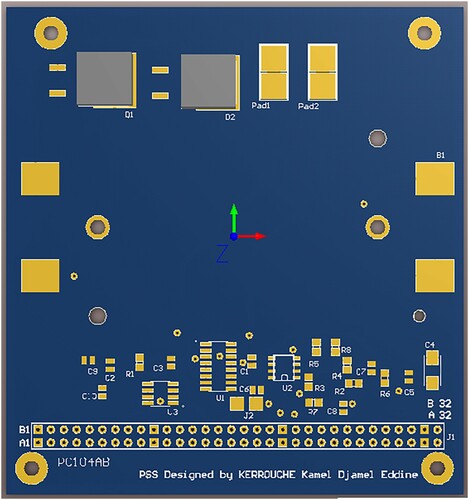
Figure 15. Electrical circuit of DC-DC boost converter connected with solar panels.
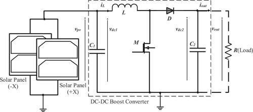
Table 5. Boost converter parameter expressions for high and low duty cycles.
Table 6. Parameters of boost converter obtained from the high and low duty cycle.
Table 7. DMC verification of boost converter obtained for high and low duty cycle.
Figure 16. Simulation of the boost converter with high duty cycle and low duty cycle: (Dashed line) Output currents; (Solid line with dots) Output voltages.
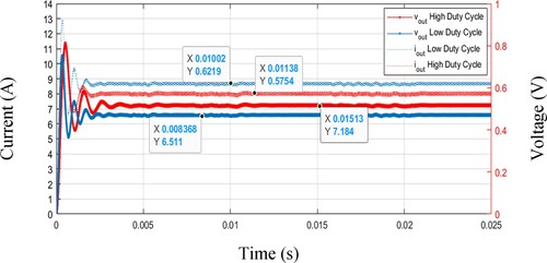
Figure 17. Electrical schematic of the Power Regulator Unit-based boost converters.
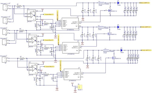
Figure 18. Power Regulation Unit’s PCB.
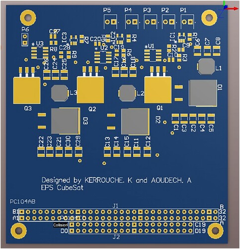
Figure 19. Flowchart of power regulation algorithm based on MPPT and BCR implemented in MCU.
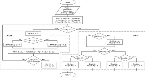
Figure 20. Simulation of MCU circuit programmed with MPPT and BCR functions.
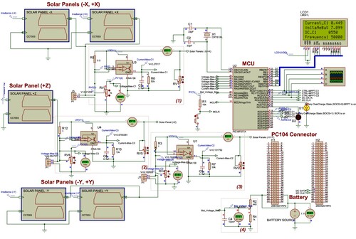
Figure 21. Simulation of MCU failure case: Boost converter driven by PWM signal from analogue MPPT selected by the arbitrating system.
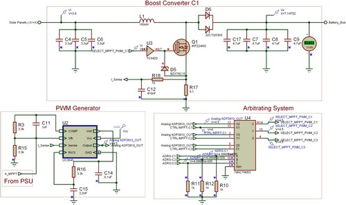
Table 8. Truth table of arbitrating system for cold redundancy.
Figure 22. EPS design ETB: (a): (1): Computer; (2): Voltmeter; (3): Battery and Power Storage Unit; (4): MCU; (5): Power Regulation Unit; (6): Programmer and Debugging system; (7): Oscilloscope; (8) Power supply; (b): (9) Lighting system; (10): Assembled solar panel.
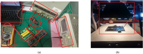
Figure 23. Line-up test block diagram of all EPS parts.
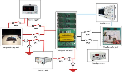
Figure 24. EL testing: (a) one solar cell, (b) one solar panel.
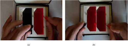
Figure 25. Solar panel characterization obtained from illumination test.
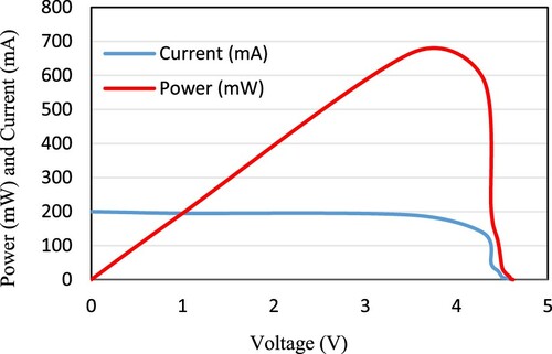
Figure 26. Experimental tests of the batteries: (a) charging characteristic; (b) discharging characteristic.
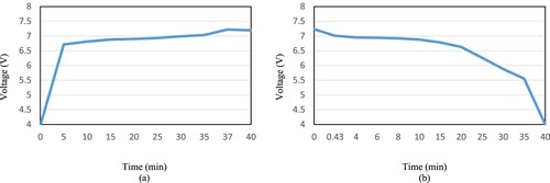
Figure 27. Charged battery level: (a) Battery voltage, (b) Voltage of electrical circuits.
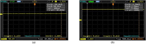
Figure 28. (a) Input voltage 3.6V, (b) Input voltage 4.35V.
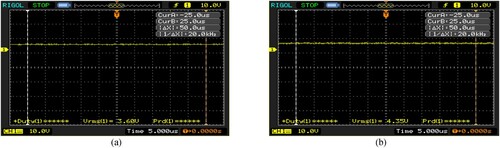
Figure 29. (a) High duty cycle PWM signal, (b) Low duty cycle PWM signal.
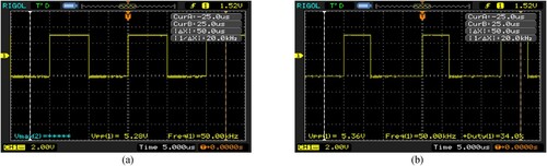
Figure 30. (a) Output voltage obtained by low duty cycle PWM signal, (b) Output voltage obtained by high duty cycle PWM signal.
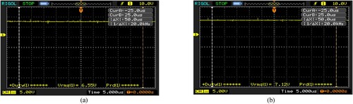
Figure 31. Output PWM obtained by MCU: (a) Low duty cycle PWM signal, (b) High duty cycle PWM signal.
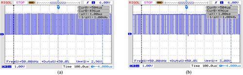
Table 9. Costs of EPS units.
Figure 32. Distribution cost: (a) Solar panel, (b) PSU, (c) PRU and (d) MCU.
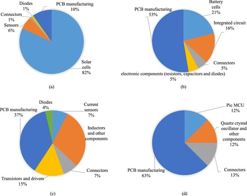
Table A1. Electrical characteristics of solar cells [Citation37].
Table A2. Electrical characteristics of battery cells [Citation46].
Figure A1. PIC16F877A pin connections.
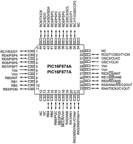
Table A3. Acronyms list.