Figures & data
Figure 1. Proposed system circuit diagram.
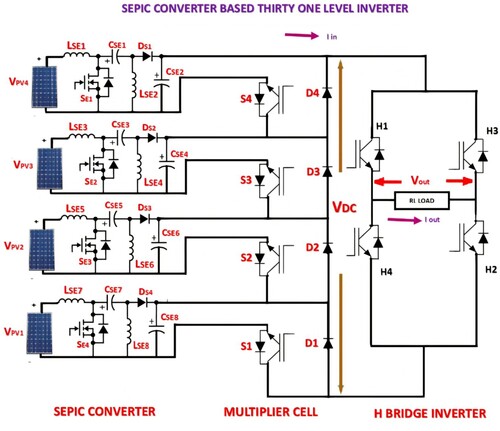
Figure 2. One diode model of the PV system.
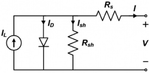
Figure 3. Proposed SEPIC converter circuit diagram.
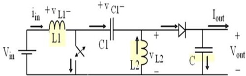
Figure 4. (a) Comparing the tracking capabilities of the different converters. (b) Efficiencies of four DC–DC converter configurations.
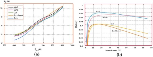
Figure 5. Flow chart for GWO-based optimization algorithm.
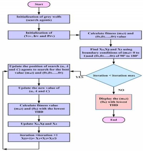
Table 1. Firing sequence of proposed 31-level inverter.
Figure 6. Angle generation for 31-level inverter.
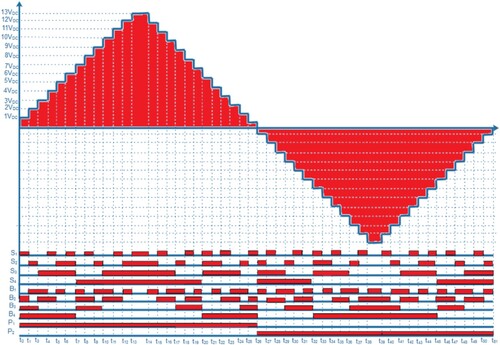
Figure 7. Flow chart for ABC-based optimization algorithm.
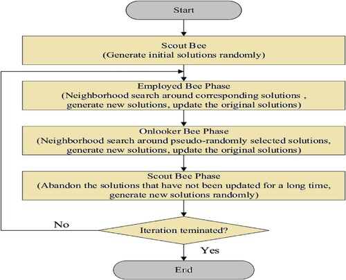
Table 2. Solar panel rating details.
Figure 8. (a) Simulation result of PV panel output voltage waveform (b) Hardware result of PV panel output voltage waveform.
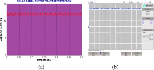
Table 3. SEPIC converter elements table.
Figure 9. Matlab simulation result (a) 6 V DC voltage to MLI (b) 12 V DC voltage to MLI (c) 24 V DC voltage to MLI (d) 48 V DC voltage to MLI.
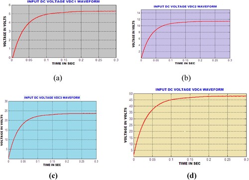
Figure 10. Hardware result (a) 6 V DC voltage to MLI (b) 12 V DC voltage to MLI (c) 24 V DC voltage to MLI (d) 48 V DC voltage to MLI.
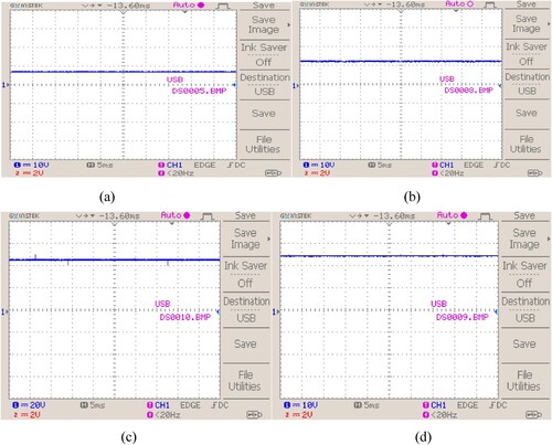
Figure 11. Proposed 31-level inverter output voltage waveform (a) Matlab Simulation (b) hardware implementation.
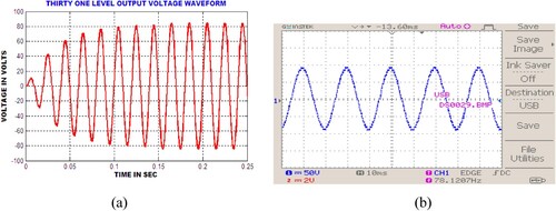
Figure 12. Simulation THD result of 31-level inverter using MCM technique.
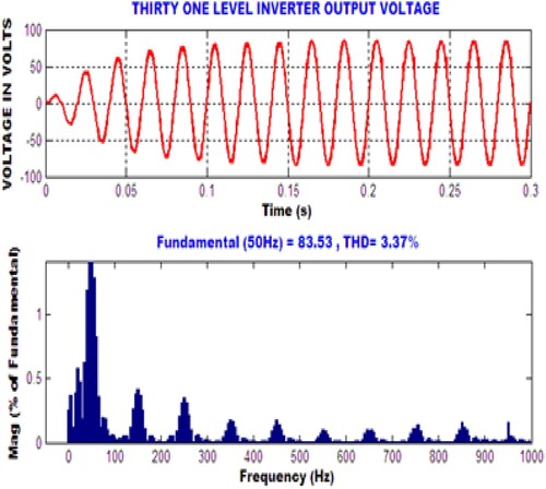
Table 4. Angle generation for 31-level inverter using SHE technique.
Figure 13. (a) Simulation output voltage 31-level inverter using ABC based SHE technique (b) Hardware output voltage 31-level inverter using ABC based SHE (c) FFT analyse of proposed 31-level inverter using ABC-SHE technique.
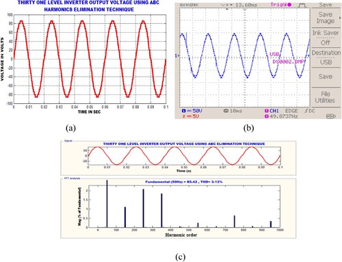
Figure 14. (a) Simulation output voltage 31-level inverter using GA technique (b) Hardware output voltage 31-level inverter using GA (c) FFT analyse of 31-level inverter using GA technique.
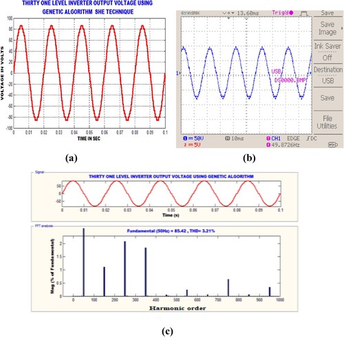
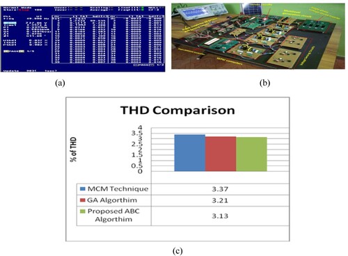
Figure 15. Experimental THD analyse of proposed MLI (b) Experimental prototype for proposed 31-level MLI system (c) THD comparison.