Figures & data
Figure 1. Simplified diagram of the proposed three-phase structure.
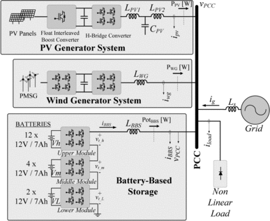
Figure 2. Control strategy applied to the BBS.
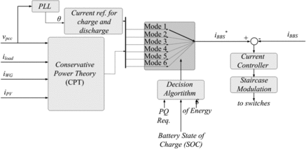
Figure 3. Principle of operation of the staircase modulation.
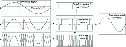
Figure 4. Voltage and current across a switch during a turn-on transition.
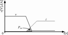
Figure 5. The flow chart of the decision algorithm.
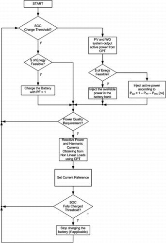
Figure 6. The SOC curve and the threshold points used in the decision algorithm.
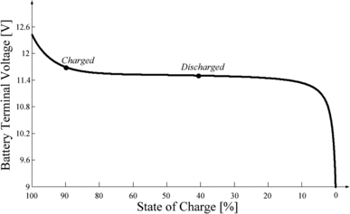
Figure 7. Third-order model of lead acid batteries.
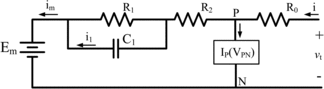
Figure 8. Wind turbine model and control scheme.
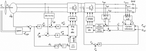
Figure 9. α-axis control loop.
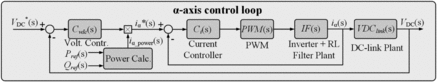
Figure 10. Bode diagram for the current loop.
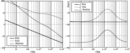
Figure 11. Bode diagram for the voltage loop.
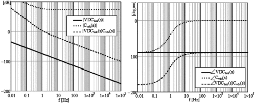
Table 1. PMSG parameters and wind turbine specifications.
Figure 12. Measured (red) and reference (blue) rotor speed in rad/s.
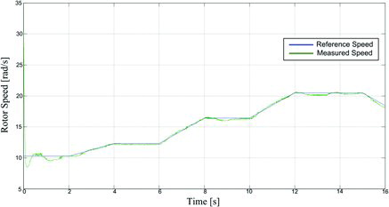
Figure 13. DC-link voltage in steady-state condition.
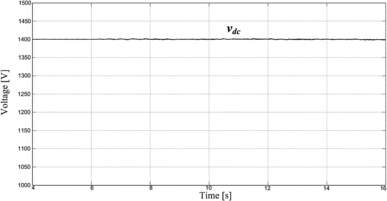
Figure 14. The three-phase PCC voltage and the WG three-phase output current in steady-state condition.
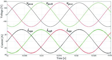
Figure 15. Schematic of the proposed power electronic interface for grid-connected PV-based system and its control strategy.
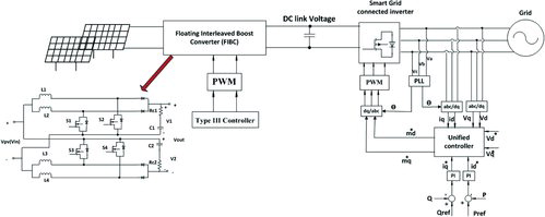
Table 2. Parameters of the type-III compensator.
Figure 16. The FIBC output voltage in steady-state condition when the PV system is injecting 2 kW into the grid.
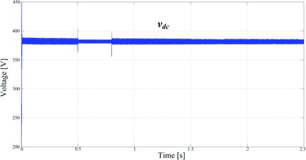
Table 3. Parameters of FIBC.
Table 4. Parameters of the inverter.
Figure 17. The three-phase PCC voltage and the three-phase PV system output current in steady-state condition.
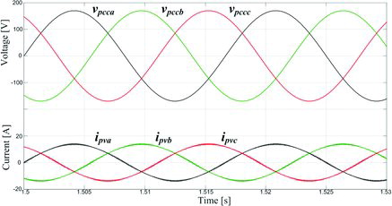
Table 5. Prototype parameters.
Figure 18. The PV, the WG and the BBS output power, as well as the sum of them for phase A.
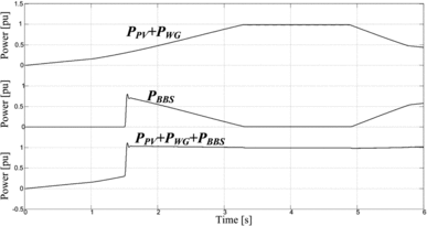
Figure 19. Three-phase PCC voltage and the three-phase BBS output current in steady-state condition under mode 2.
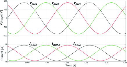
Figure 20. BBS terminal voltage for each module for phase A.
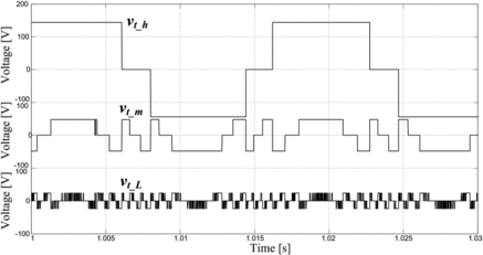
Figure 21. The PCC voltage, the BBS current and the grid current when the BBS during the transition from mode 2 to mode 4.
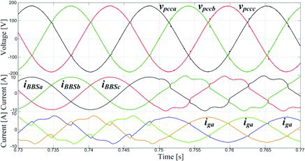
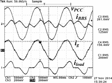
Figure 22. PCC voltage, BBS output current and the load current during transition from mode 2 to mode 1.
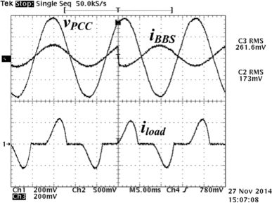
Figure 23. The BBS terminal voltage (vt) and the cell output voltages (vt_h, vt_m and vt_L) (R1, R2, R3, Ch4: 500 mV/250 V).
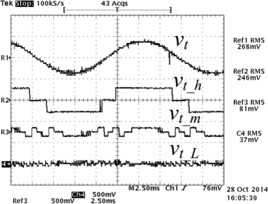
Figure 24. The BBS output current measured in a long timescale and a detail of a short period when the WG and PV systems are emulated, mode 3 (Ch1: 0.1 V/A).
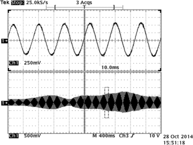
Figure 25. PCC voltage, the BBS, the grid and load currents when the BBS is operating exclusively as active filter (mode 6).