
Figures & data
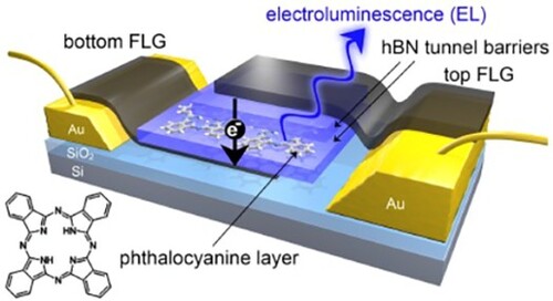
Figure 1. FLG/hBN/H2Pc/hBN/FLG heterostructures. a Schematic of device in which a monolayer of H2Pc is encapsulated between two hBN tunnel barriers and charge can be transported between upper and lower FLG contacts under the application of an applied bias; lower left – schematic of the molecular structure of H2Pc. b AFM image of a monolayer coverage of H2Pc on hBN. Inset, high resolution image with schematic overlay. c Optical image of a device showing gold contacts and the van der Waals heterostructure. The dashed line indicates the active area of the device where the upper and lower FLG layers overlap. Inset top: SEM image of the highlighted area in false colour showing the FLG (grey) and hBN layers (blue). Inset bottom: scanning electroluminescence image taken at a +2.2 V bias and 1 s integration time confirming that light is emitted from the active area of the device. d current–voltage (black) and differential current-voltage (blue) characteristics. Inset: current-voltage on a logarithmic scale. e Electroluminescence spectrum. Inset, black: experimental PL spectrum, grey: fit using three Lorentzian curves with peak positions 704, 720 and 741 nm. Scale bars b 15 nm, b inset 2 nm, c main image and insets 10 μm.
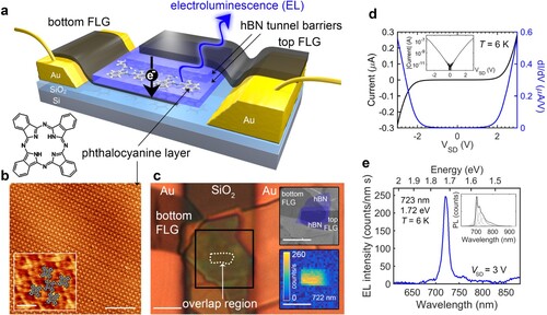
Figure 2. Electroluminescence in FLG/hBN/H2Pc/hBN/FLG heterostructures measured at room temperature. Colour map of the EL spectra as a function of applied bias. White circles, right axis: integrated intensity of EL over the wavelength range 700–750 nm.
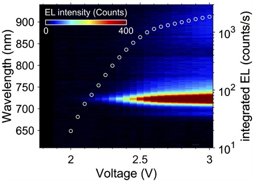
Figure 3. Electroluminescence spectra acquired at T = 6 ± 2 K from a FLG/hBN/H2Pc/hBN/FLG heterostructure device for a series of bias voltages ranging from −1.5 to −1.9 V. The bias voltage and acquisition time for each spectrum is annotated in the corresponding colour. The spectra acquired at −1.6 and −1.7 V exhibit photon up-conversion.
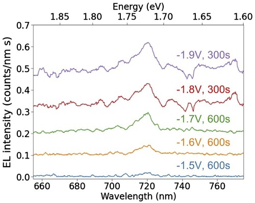
Figure 4. a Dependence of EL intensity on current; b Dependence of efficiency on applied voltage. Data are acquired at room temperature.
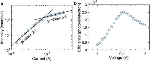
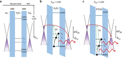
Figure 5. Energy level diagrams for a H2Pc tunnelling device under zero bias (a), 1.6V bias (b), and a PTCDI tunnelling device under 1.6V bias (c). Inelastic electron scattering (IES) events are labelled. (a) Under zero bias both the H2Pc singlet, S1, and triplet, T1, states lie below the Fermi energy of the bottom graphene electrode, . (b) At 1.6V bias, T1 lies 100 meV above
. Up-converted electroluminescence from S1 is observed at 1.6V bias. (c) The lower-lying energy levels of PTCDI mean that under 1.6V bias, both S1 and T1 lie below
and emission is observed from both states.
Supplemental Material
Download MS Word (1.8 MB)Data availability statement
The authors declare that the data supporting the findings of this study are available within the article and its Supplementary Information files, or from the corresponding author on reasonable request.